


74AC138SJX
Fairchild Semiconductor 74AC138SJX, 74AC138SJ, 74AC138SCX, 74AC138SC, 74AC138PC Datasheet
...
© 2000 Fairchild Semiconductor Corporation DS009925 www.fairchildsemi.com
November 1988
Revised August 2000
74AC138 • 74ACT138 1-of-8 Decoder/Demultiplexer
74AC138 • 74ACT138
1-of-8 Decoder/Demultiplexer
General Description
The AC/ACT138 is a high-speed 1-of-8 decoder/d emultiplexer. This device is ideally suited for hi gh-speed bipolar
memory chip select address decoding. The multiple input
enables allow parallel expansion to a 1-of-24 decoder
using just three AC/ACT138 d evices or a 1-of-32 de coder
using four AC/ACT138 devices and one inverter.
Features
■ ICC reduced by 50%
■ Demultiplexing capability
■ Multiple input enable for easy expansion
■ Active LOW mutually exclusive outputs
■ Outputs source/sink 24 mA
■ ACT138 has TTL-compatible inputs
Ordering Code:
Device also available in Tape and Reel. Specify by appending s uffix let te r “X” to the ordering code.
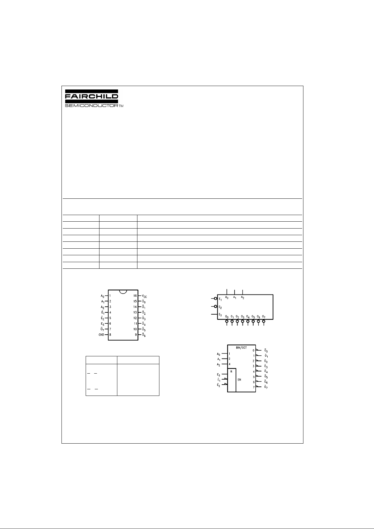
Connection Diagram
Pin Descriptions
Logic Symbols
IEEE/IEC
FACT is a trademark of Fairchild Semiconductor Corporation.
Order Number Package Number Package Description
74AC138SC M16A 16-Lead Small Outline Integrated Circuit (SOIC), JEDEC MS-012, 0.150 Narrow
74AC138SJ M16D 16-Lead Small Outline Package (SOP), EIAJ TYPE II, 5.3mm Wide
74AC138MTC MTC16 16-Lead Thin Shrink Small Outline Package (TSSOP), JEDEC MO-153, 4.4mm Wide
74AC138PC N16E 16-Lead Plastic Dual-In-Line Package (PDIP), JEDEC MS-001, 0.300 Wide
74ACT138SC M16A 16-Lead Small Outline Integrated Circuit (SOIC), JEDEC MS-012, 0.150 Narrow
74ACT138SJ M16D 16-Lead Small Outline Package (SOP), EIAJ TYPE II, 5.3mm Wide
74ACT138PC N16E 16-Lead Plastic Dual-In-Line Package (PDIP), JEDEC MS-001, 0.300 Wide
Pin Names Description
A
0–A2
Address Inputs
E
1–E2
Enable Inputs
E
3
Enable Input
O
0–O7
Outputs
www.fairchildsemi.com 2
74AC138 • 74ACT138
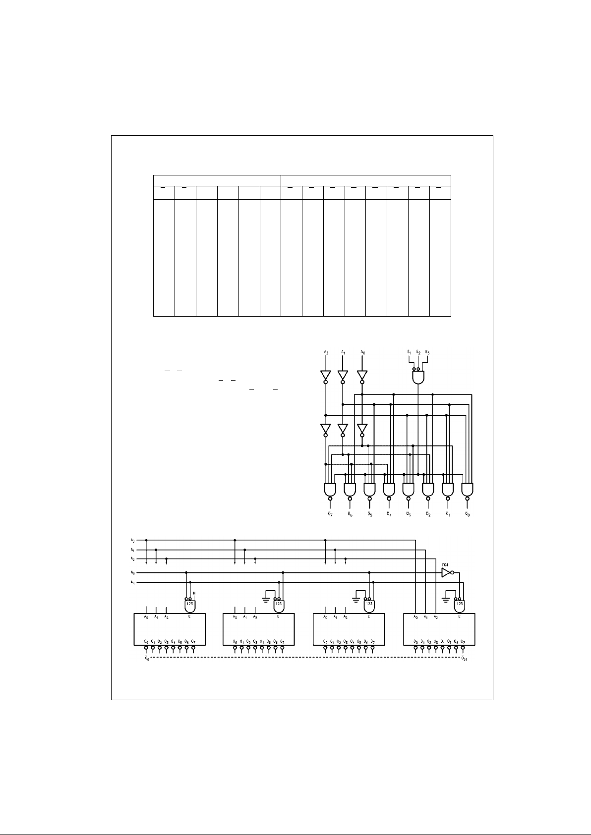
Truth Table
H = HIGH Voltage Level L = LOW Voltage Level X = Immaterial
Functional Description
The AC/ACT138 high -speed 1-of-8 decoder/de multiplexer
accepts three binary weighted inputs (A
0
, A1, A2) and,
when enabled, provides eight mutually exclusive activeLOW outputs (O
0–O7
). The AC/ACT138 features three
Enable inputs, two active-LOW (E
1
, E2) and one active-
HIGH (E
3
). All outputs will be HIGH unless E1 and E2 are
LOW and E
3
is HIGH. This multiple enable fun ction allows
easy parallel expansion of the device to a 1-of-32 (5 lin es
to 32 lines) decoder with j u st fo ur AC/A CT1 38 d evice s an d
one inverter (see Figure 1). The AC/ACT 138 can be used
as an 8-output demultiplexer by using one of the ac tive
LOW Enable inputs as the data input and the oth er E nab le
inputs as strobes. The En able inputs which are not used
must be permanently tied to their appro priate active- HIGH
or active-LOW state.
Logic Diagram
Please note that this diagram is provided only for the understanding of logic
operations and should not be used to estimate propagation delays.
FIGURE 1. Expans ion to 1-of-32 De coding
Inputs Outputs
E
1E2E3A0A1A2O0O1O2O3O4O5O6O7
HXXXXXHHHHHHHH
XHXXXXHHHHHHHH
XXLXXXHHHHHHHH
LLHLLLLHHHHHHH
LLHHLLHLHHHHHH
LLHLHLHHLHHHHH
LLHHHLHHHLHHHH
LLHLLHHHHHLHHH
LLHHLHHHHHHLHH
LLHLHHHHHHHHLH
LLHHHHHHHHHHHL
3 www.fairchildsemi.com
74AC138 • 74ACT138
Absolute Maximum Ratings(Note 1) Recommended Operating
Conditions
Note 1: Absolute max imum ratings are those values beyond w hich damage
to the device may occu r. The databook spe cificatio ns shou ld be met, wit hout exception, to ensure that the system de sign is relia ble over its p ower
supply, temperature, and output/input loading variables. Fairchild does not
recommend operation of FACT circuits outside databook specif ic at ions.
DC Electrical Characteristics for AC
Note 2: All outputs loaded; thres holds on input associate d w it h output under test.
Note 3: Maximum test duration 2.0 ms, one output loaded at a time.
Note 4: I
IN
and ICC @ 3.0V are guaranteed to be less than or equa l t o th e respective limit @ 5.5V VCC.
Supply Voltage (VCC) −0.5V to +7.0V
DC Input Diode Current (I
IK
)
V
I
= −0.5V −20 mA
V
I
= VCC + 0.5V +20 mA
DC Input Voltage (V
I
) −0.5V to VCC + 0.5V
DC Output Diode Current (I
OK
)
V
O
= −0.5V −20 mA
V
O
= VCC + 0.5V +20 mA
DC Output Voltage (V
O
) −0.5V to VCC + 0.5V
DC Output S ource
or Sink Current (I
O
) ±50 mA
DC V
CC
or Ground Current
per Output Pin (I
CC
or I
GND
) ±50 mA
Storage Temperature (T
STG
) −65°C to +150°C
Junction Temperature (T
J
)
PDIP 140
°C
Supply Voltage (V
CC
)
AC 2.0V to 6.0V
ACT 4.5V to 5.5V
Input Voltage (V
I
)0V to V
CC
Output Voltage (VO)0V to V
CC
Operating Temperature (TA) −40°C to +85°C
Minimum Input Edge Rate (
∆V/∆t)
AC Devices
V
IN
from 30% to 70% of V
CC
VCC @ 3.3V, 4.5V, 5.5V 125 mV/ns
Minimum Input Edge Rate (
∆V/∆t)
ACT Devices
V
IN
from 0.8V to 2.0V
V
CC
@ 4.5V, 5.5V 125 mV/ns
Symbol Parameter
V
CC
TA = +25°CT
A
= −40°C to +85°C
Units Conditions
(V) Typ Guaranteed Limits
V
IH
Minimum HIGH Level 3.0 1.5 2.1 2.1 V
OUT
= 0.1V
Input Voltage 4.5 2.25 3.15 3.15 V or VCC − 0.1V
5.5 2.75 3.85 3.85
V
IL
Maximum LOW Level 3.0 1.5 0.9 0.9 V
OUT
= 0.1V
Input Voltage 4.5 2.25 1.35 1.35 V or VCC − 0.1V
5.5 2.75 1.65 1.65
V
OH
Minimum HIGH Level 3.0 2.99 2.9 2.9
Output Voltage 4.5 4.49 4.4 4.4 V I
OUT
= −50 µA
5.5 5.49 5.4 5.4
VIN = VIL or V
IH
3.0 2.56 2.46 IOH = −12 mA
4.5 3.86 3.76 V I
OH
= −24 mA
5.5 4.86 4.76 I
OH
= −24 mA (Note 2)
V
OL
Maximum LOW Level 3.0 0.002 0.1 0.1
Output Voltage 4.5 0.001 0.1 0.1 V I
OUT
= 50 µA
5.5 0.001 0.1 0.1
VIN = VIL or V
IH
3.0 0.36 0.44 IOL = 24 mA
4.5 0.36 0.44 V IOL = 24 mA 0
5.5 0.36 0.44 IOL = 24 mA (Note 2)
IIN Maximum Input
5.5 ±0.1 ±1.0 µAVI = VCC, GND
(Note 4) Leakage Current
I
OLD
Minimum Dynamic 5.5 75 mA V
OLD
= 1.65V Max
I
OHD
Output Current (Note 3) 5.5 −75 mA V
OHD
= 3.85V Min
I
CC
(Note 4)
Maximum Quiescent
Supply Current
5.5 4.0 40.0 µAVIN = VCC or GND
 Loading...