


Fairchild Semiconductor 74AC174MTCX, 74AC174MTC, 74AC174CW, 74AC174SJX, 74AC174SJ Datasheet
...
November 1988
Revised November 1999
74AC174 • 74ACT174
Hex D-Type Flip-Flop with Master Reset
General Description
The AC/ACT174 is a high-speed hex D-type flip-flop. The device is used primarily as a 6-bit edge-triggered storage register. The information on the D inputs is transferred to storage during the LOW-to-HIGH clock transition. The device has a Master Reset to simultaneously clear all flipflops.
Features
■ICC reduced by 50%
■Outputs source/sink 24 mA
■ACT174 has TTL-compatible inputs
Ordering Code:
Order Number |
Package Number |
Package Description |
|
|
|
74AC174SC |
M16A |
16-Lead Small Outline Integrated Circuit (SOIC), JEDEC MS-012, 0.150” Narrow Body |
|
|
|
74AC174SJ |
M16D |
16-Lead Small Outline Package (SOP), EIAJ TYPE II, 5.3mm Wide |
|
|
|
74AC174PC |
N16E |
16-Lead Plastic Dual-In-Line Package (PDIP), JEDEC MS-001, 0.300” Wide |
|
|
|
74ACT174SC |
M16A |
16-Lead Small Outline Integrated Circuit (SOIC), JEDEC MS-012, 0.150” Narrow |
|
|
|
74ACT174SJ |
M16D |
16-Lead Small Outline Package (SOP), EIAJ TYPE II, 5.3mm Wide |
|
|
|
74ACT174MTC |
MTC16 |
16-Lead Thin Shrink Small Outline Package (TSSOP), JEDEC MO-153, 4.4mm Wide |
|
|
|
74ACT174PC |
N16E |
16-Lead Plastic Dual-In-Line Package (PDIP), JEDEC MS-001, 0.300” Wide |
|
|
|
Device also available in Tape and Reel. Specify by appending suffix letter “X” to the ordering code.
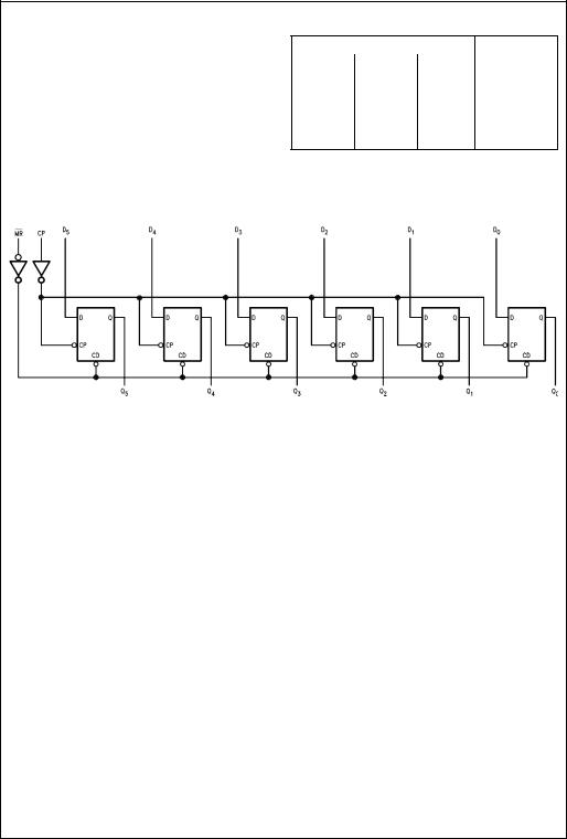
Logic Symbols |
Connection Diagram |
IEEE/IEC
Pin Descriptions
|
Pin Names |
Description |
|
|
|
|
|
|
D0–D5 |
Data Inputs |
|
|
CP |
Clock Pulse Input |
|
|
|
Master Reset Input |
|
|
MR |
|
|
|
Q0–Q5 |
Outputs |
|
FACT is a trademark of Fairchild Semiconductor Corporation.
Reset Master with Flop-Flip Type-D Hex 74ACT174 • 74AC174
© 1999 Fairchild Semiconductor Corporation |
DS009935 |
www.fairchildsemi.com |
74AC174 • 74ACT174
Functional Description
The AC/ACT174 consists of six edge-triggered D-type flipflops with individual D inputs and Q outputs. The Clock (CP) and Master Reset (MR) are common to all flip-flops. Each D input’s state is transferred to the corresponding flipflop’s output following the LOW-to-HIGH Clock (CP) transition. A LOW input to the Master Reset (MR) will force all outputs LOW independent of Clock or Data inputs. The AC/ ACT174 is useful for applications where the true output only is required and the Clock and Master Reset are common to all storage elements.
Logic Diagram
Truth Table
|
|
Inputs |
|
Output |
|
|
|
|
|
|
MR |
CP |
D |
Q |
|
|
|
|
|
|
L |
X |
X |
L |
|
H |
|
H |
H |
|
H |
|
L |
L |
|
H |
L |
X |
Q |
H = HIGH Voltage Level
L = LOW Voltage Level
= LOW-to-HIGH Transition
X = Immaterial
Please note that this diagram is provided only for the understanding of logic operations and should not be used to estimate propagation delays.
www.fairchildsemi.com |
2 |

Absolute Maximum Ratings(Note 1)
Supply Voltage (VCC) |
− 0.5V to + 7.0V |
|
DC Input Diode Current (IIK) |
|
|
VI = |
− 0.5V |
− 20 mA |
VI = |
VCC + 0.5V |
+ 20 mA |
DC Input Voltage (VI) |
− 0.5V to VCC + 0.5V |
|
DC Output Diode Current (IOK) |
|
|
VO = − 0.5V |
− 20 mA |
|
V = |
VCC + 0.5V |
+ 20 mA |
DC Output Voltage (VO) |
− 0.5V to V CC + 0.5V |
|
DC Output Source |
|
|
or Sink Current (IO) |
± 50 mA |
|
DC VCC or Ground Current |
|
|
per Output Pin (ICC or IGND) |
± 50 mA |
|
Storage Temperature (TSTG) |
− 65° C to + 150° C |
|
Junction Temperature (TJ) |
|
|
PDIP |
140° C |
|
Recommended Operating
Conditions
Supply Voltage (VCC) |
|
AC |
2.0V to 6.0V |
ACT |
4.5V to 5.5V |
Input Voltage (VI) |
0V to VCC |
Output Voltage (VO) |
0V to VCC |
Operating Temperature (TA) |
− 40° C to + 85° C |
Minimum Input Edge Rate (∆ V/∆ t) |
|
AC Devices |
|
VIN from 30% to 70% of VCC |
|
VCC @ 3.3V, 4.5V, 5.5V |
125 mV/ns |
Minimum Input Edge Rate (∆ V/∆ t) |
|
ACT Devices |
|
VIN from 0.8V to 2.0V |
|
VCC @ 4.5V, 5.5V |
125 mV/ns |
Note 1: Absolute maximum ratings are those values beyond which damage to the device may occur. The databook specifications should be met, without exception, to ensure that the system design is reliable over its power supply, temperature, and output/input loading variables. Fairchild does not recommend operation of FACT circuits outside databook specifications.
DC Electrical Characteristics for AC
Symbol |
Parameter |
VCC |
TA = + 25° C |
|
TA = − 40° C to + 85° C |
Units |
Conditions |
|||
|
|
(V) |
Typ |
|
Guaranteed Limits |
|
|
|
|
|
|
|
|
|
|
|
|
|
|
||
VIH |
Minimum HIGH Level |
3.0 |
1.5 |
2.1 |
|
2.1 |
|
VOUT = |
0.1V |
|
|
Input Voltage |
4.5 |
2.25 |
3.15 |
|
3.15 |
V |
or VCC − |
0.1V |
|
|
|
5.5 |
2.75 |
3.85 |
|
3.85 |
|
|
|
|
|
|
|
|
|
|
|
|
|
|
|
VIL |
Maximum LOW Level |
3.0 |
1.5 |
0.9 |
|
0.9 |
|
VOUT = |
0.1V |
|
|
Input Voltage |
4.5 |
2.25 |
1.35 |
|
1.35 |
V |
or VCC − |
0.1V |
|
|
|
5.5 |
2.75 |
1.65 |
|
1.65 |
|
|
|
|
|
|
|
|
|
|
|
|
|
|
|
VOH |
Minimum HIGH Level |
3.0 |
2.99 |
2.9 |
|
2.9 |
|
|
|
|
|
Output Voltage |
4.5 |
4.49 |
4.4 |
|
4.4 |
V |
IOUT = |
− |
50 µ A |
|
|
5.5 |
5.49 |
5.4 |
|
5.4 |
|
|
|
|
|
|
|
|
|
|
|
|
|
||
|
|
|
|
|
|
|
|
VIN = VIL or VIH |
||
|
|
3.0 |
|
2.56 |
|
2.46 |
|
IOH = − 12 mA |
||
|
|
4.5 |
|
3.86 |
|
3.76 |
V |
IOH = − 24 mA |
||
|
|
5.5 |
|
4.86 |
|
4.76 |
|
IOH = − 24 mA (Note 2) |
||
VOL |
Maximum LOW Level |
3.0 |
0.002 |
0.1 |
|
0.1 |
|
|
|
|
|
Output Voltage |
4.5 |
0.001 |
0.1 |
|
0.1 |
V |
IOUT = |
50 µ A |
|
|
|
5.5 |
0.001 |
0.1 |
|
0.1 |
|
|
|
|
|
|
|
|
|
|
|
|
|
||
|
|
|
|
|
|
|
|
VIN = VIL or VIH |
||
|
|
3.0 |
|
0.36 |
|
0.44 |
|
IOL = 12 mA |
||
|
|
4.5 |
|
0.36 |
|
0.44 |
V |
IOL = 24 mA |
||
|
|
5.5 |
|
0.36 |
|
0.44 |
|
IOL = 24 mA (Note 2) |
||
IIN |
Maximum Input |
5.5 |
|
± 0.1 |
|
± 1.0 |
µ A |
VI = VCC |
||
(Note 4) |
Leakage Current |
|
|
or GND |
|
|||||
|
|
|
|
|
|
|
||||
|
|
|
|
|
|
|
|
|
|
|
IOLD |
Minimum Dynamic |
5.5 |
|
|
|
75 |
mA |
VOLD = |
1.65V Max |
|
IOHD |
Output Current (Note 3) |
5.5 |
|
|
|
− 75 |
mA |
VOHD = |
|
3.85V Min |
ICC |
Maximum Quiescent |
5.5 |
|
4.0 |
|
40.0 |
µ A |
VIN = VCC |
||
(Note 4) |
Supply Current |
|
|
or GND |
||||||
|
|
|
|
|
|
|||||
|
|
|
|
|
|
|
|
|
|
|
Note 2: All outputs loaded; thresholds on input associated with output under test.
Note 3: Maximum test duration 2.0 ms, one output loaded at a time.
Note 4: IIN and ICC @ 3.0V are guaranteed to be less than or equal to the respective limit @ 5.5V VCC.
74ACT174 • 74AC174
3 |
www.fairchildsemi.com |
 Loading...