


February 1990
Revised August 2000
100370
Low Power Universal Demultiplexer/Decoder
General Description
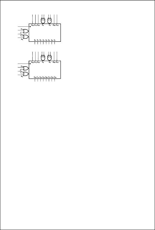
The 100370 universal demultiplexer/decoder functions as either a dual 1-of-4 decoder or as a single 1-of-8 decoder, depending on the signal applied to the Mode Control (M) input. In the dual mode, each half has a pair of active-LOW Enable (E) inputs. Pin assignments for the E inputs are such that in the 1-of-8 mode they can easily be tied together in pairs to provide two active-LOW enables (E1a to
E1b, E2a to E2b). Signals applied to auxiliary inputs Ha, Hb and Hc determine whether the outputs are active HIGH or
active LOW. In the dual 1-of-4 mode the Address inputs are A0a, A1a and A0b, A1b with A2a unused (i.e., left open, tied to VEE or with LOW signal applied). In the 1-of-8 mode, the
Address inputs are A0a, A1a, A2a with A0b and A1b LOW or OPEN. All inputs have 50 kΩ pull-down resistors.
Features
■35% power reduction of the 100170
■2000V ESD protection
■Pin/function compatible with 100170
■Voltage compensated operating range = − 4.2V to − 5.7V
Ordering Code:
Order Number |
Package Number |
Package Description |
|
|
|
100370PC |
N24E |
24-Lead Plastic Dual-In-Line Package (PDIP), JEDEC MS-010, 0.400 Wide |
|
|
|
100370QC |
V28A |
28-Lead Plastic Lead Chip Carrier (PLCC), JEDEC MO-047, 0.450 Square |
|
|
|
100370QI |
V28A |
28-Lead Plastic Lead Chip Carrier (PLCC), JEDEC MO-047, 0.450 Square |
|
|
Industrial Temperature Range (− 40° C to + 85° C) |
|
|
|
Devices also available in Tape and Reel. Specify by appending the suffix letter “X” to the ordering code.
Connection Diagrams
24-Pin DIP 28-Pin PLCC
Demultiplexer/Decoder Universal Power Low 100370
© 2000 Fairchild Semiconductor Corporation |
DS010649 |
www.fairchildsemi.com |
100370
Logic Symbols |
Pin Descriptions |
||||||||||
|
|
|
|
|
|
|
|
||||
Single 1-of 8 Application |
|
|
Pin Names |
|
|
|
Description |
||||
|
|
|
Ana, Anb |
Address Inputs |
|||||||
|
|
|
E |
na, |
E |
nb |
Enable Inputs |
||||
|
|
|
M |
Mode Control Input |
|||||||
|
|
|
Ha |
|
|
|
|
|
|||
|
|
|
Z0–Z3 (Z |
0a–Z3a) Polarity Select Input |
|||||||
|
|
|
Hb |
|
|
|
|
|
|||
|
|
|
Z4–Z7 (Z |
0b–Z3b) Polarity Select Input |
|||||||
|
|
|
Hc |
Common Polarity Select Input |
|||||||
|
|
|
Z0–Z7 |
Single 1-of-8 Data Outputs |
|||||||
Dual 1-of-4 Application- |
|
|
Zna, Znb |
Dual 1-of-4 Data Outputs |
|||||||
|
|
|
|
|
|
|
|
|
|
|
|
Truth Tables
|
|
|
|
|
|
|
|
|
|
Dual 1-of-4 Mode (M = |
A2a = |
Hc = |
|
|
LOW) |
|
|
|
|
|
|
|
||||||||||||||
|
|
|
|
|
|
|
|
|
|
|
|
|
|
|
|
|
|
|
|
|
|
|
|
|
|
|
|
|
|
|
||||||
|
|
|
|
|
|
|
|
Inputs |
|
|
|
Active HIGH Outputs |
|
|
|
|
Active LOW Outputs |
|||||||||||||||||||
|
|
|
|
|
|
|
|
|
|
|
|
|
(Ha and Hb Inputs HIGH) |
|
(Ha and Hb Inputs LOW) |
|||||||||||||||||||||
|
|
|
|
|
|
|
|
|
|
|
|
|
|
|
|
|
|
|
|
|
|
|
|
|
|
|
|
|
|
|
|
|
|
|
||
|
|
E1a |
|
|
E2a |
A1a |
|
A0a |
|
Z0a |
Z1a |
Z2a |
|
|
Z3a |
|
|
|
Z0a |
|
Z1a |
|
Z2a |
|
Z3a |
|||||||||||
|
|
|
|
|
|
|
|
|
|
|
|
|
|
|
|
|
|
|
|
|
|
|
|
|
|
|
|
|
|
|
|
|
|
|
||
|
E1b |
|
|
E2b |
A1b |
|
A0b |
|
Z0b |
Z1b |
Z2b |
|
|
Z3b |
|
|
|
Z0b |
|
Z1b |
|
Z2b |
|
Z3b |
||||||||||||
|
|
H |
|
|
X |
X |
|
X |
|
L |
L |
|
L |
|
|
L |
|
|
|
|
H |
|
|
H |
|
H |
|
H |
||||||||
|
|
X |
|
|
H |
X |
|
X |
|
L |
L |
|
L |
|
|
L |
|
|
|
|
H |
|
|
H |
|
H |
|
H |
||||||||
|
|
|
|
|
|
|
|
|
|
|
|
|
|
|
|
|
|
|
|
|
|
|
|
|
|
|
|
|
|
|
|
|
||||
|
|
L |
|
|
L |
L |
|
L |
|
H |
L |
|
L |
|
|
L |
|
|
|
|
L |
|
|
H |
|
H |
|
H |
||||||||
|
|
L |
|
|
L |
L |
|
H |
|
L |
H |
|
L |
|
|
L |
|
|
|
|
H |
|
|
L |
|
H |
|
H |
||||||||
|
|
L |
|
|
L |
H |
|
L |
|
L |
L |
|
H |
|
|
L |
|
|
|
|
H |
|
|
H |
|
L |
|
H |
||||||||
|
|
L |
|
|
L |
H |
|
H |
|
L |
L |
|
L |
|
|
H |
|
|
|
|
H |
|
|
H |
|
H |
|
L |
||||||||
|
|
|
|
|
|
|
|
|
|
|
|
|
|
|
|
|
|
|
|
|
|
|
|
|
|
|
|
|
|
|||||||
|
|
|
|
|
|
|
Single 1-of-8 Mode (M = |
HIGH; A0b = |
A1b = |
|
|
Ha = Hb = LOW) |
|
|
||||||||||||||||||||||
|
|
|
|
|
|
|
|
|
|
|
|
|
|
|
|
|
|
|
|
|
|
|
|
|||||||||||||
|
|
|
|
|
|
|
|
|
Inputs |
|
|
|
|
|
Active HIGH Outputs (Note 1) |
|
|
|||||||||||||||||||
|
|
|
|
|
|
|
|
|
|
|
|
|
|
|
|
|
|
|
|
|
(Hc Input HIGH) |
|
|
|
|
|||||||||||
|
|
|
|
|
|
|
|
|
|
|
|
|
|
|
|
|
|
|
|
|
|
|
|
|
|
|
|
|
|
|
||||||
|
|
E1 |
|
|
E2 |
A2a |
|
A1a |
|
A0a |
|
Z0 |
|
Z1 |
|
Z2 |
|
Z3 |
|
Z4 |
|
Z5 |
|
Z6 |
|
Z7 |
||||||||||
|
|
H |
|
|
X |
X |
|
X |
|
X |
|
L |
|
L |
|
|
L |
|
|
L |
|
L |
|
L |
|
L |
|
L |
||||||||
|
|
X |
|
|
H |
X |
|
X |
|
X |
|
L |
|
L |
|
|
L |
|
|
L |
|
L |
|
L |
|
L |
|
L |
||||||||
|
|
|
|
|
|
|
|
|
|
|
|
|
|
|
|
|
|
|
|
|
|
|
|
|
|
|
|
|
||||||||
|
|
L |
|
|
L |
L |
|
L |
|
L |
|
H |
|
L |
|
|
L |
|
|
L |
|
L |
|
L |
|
L |
|
L |
||||||||
|
|
L |
|
|
L |
L |
|
L |
|
H |
|
L |
|
H |
|
|
L |
|
|
L |
|
L |
|
L |
|
L |
|
L |
||||||||
|
|
L |
|
|
L |
L |
|
H |
|
L |
|
L |
|
L |
|
|
H |
|
|
L |
|
L |
|
L |
|
L |
|
L |
||||||||
|
|
L |
|
|
L |
L |
|
H |
|
H |
|
L |
|
L |
|
|
L |
|
H |
|
L |
|
L |
|
L |
|
L |
|||||||||
|
|
|
|
|
|
|
|
|
|
|
|
|
|
|
|
|
|
|
|
|
|
|
|
|
|
|
|
|
||||||||
|
|
L |
|
|
L |
H |
|
L |
|
L |
|
L |
|
L |
|
|
L |
|
|
L |
|
H |
|
L |
|
L |
|
L |
||||||||
|
|
L |
|
|
L |
H |
|
L |
|
H |
|
L |
|
L |
|
|
L |
|
|
L |
|
L |
|
H |
|
L |
|
L |
||||||||
|
|
L |
|
|
L |
H |
|
H |
|
L |
|
L |
|
L |
|
|
L |
|
|
L |
|
L |
|
L |
|
H |
|
L |
||||||||
|
|
L |
|
|
L |
H |
|
H |
|
H |
|
L |
|
L |
|
|
L |
|
|
L |
|
L |
|
L |
|
L |
|
H |
||||||||
|
|
|
|
|
|
|
|
|
|
|
|
|
|
|
|
|
|
|
|
|
|
|
|
|
|
|
|
|
||||||||
H = HIGH Voltage Level |
|
L = |
LOW Voltage Level |
X = Don’t Care |
|
|
1 = |
|
1a and |
|
|
1b wired; |
|
2 = |
|
|
|
|
|
|||||||||||||||||
|
E |
E |
E |
E |
E22a and E2b wired |
|||||||||||||||||||||||||||||||
Note 1: for Hc = LOW, output states are complemented
www.fairchildsemi.com |
2 |

Logic Diagram
(Zn) for 1-of-4 applications.
100370
3 |
www.fairchildsemi.com |
 Loading...