


74AC139SJX
Fairchild Semiconductor 74AC139SJX, 74AC139SJ, 74AC139SCX, 74AC139SC, 74AC139PC Datasheet
...
© 1999 Fairchild Semiconductor Corporation DS009926 www.fairchildsemi.com
November 1988
Revised November 1999
74AC139 • 74ACT139 Dual 1-of-4 Decoder/Demultiplexer
74AC139 • 74ACT139
Dual 1-of-4 Decoder/Demultiplexer
General Description
The AC/ACT139 is a high-speed, dual 1-of-4 decoder/
demultiplexer. The device has two independent decode rs,
each accepting two inputs and providing four mutuallyexclusive active-LOW outputs. Each decoder has an
active-LOW Enable input which can be used as a data
input for a 4-output demultiplexer. Each half of the AC/
ACT139 can be used as a function gene rator providi ng all
four minterms of two variables.
Features
■ ICC reduced by 50%
■ Multifunction capability
■ Two completely independent 1-of-4 decoders
■ Active LOW mutually exclusive outputs
■ Outputs source/sink 24 mA
■ ACT139 has TTL-compatible inputs
Ordering Code:
Device also available in Tape and Reel. Specify by appending s uffix let te r “X” to the ordering code.
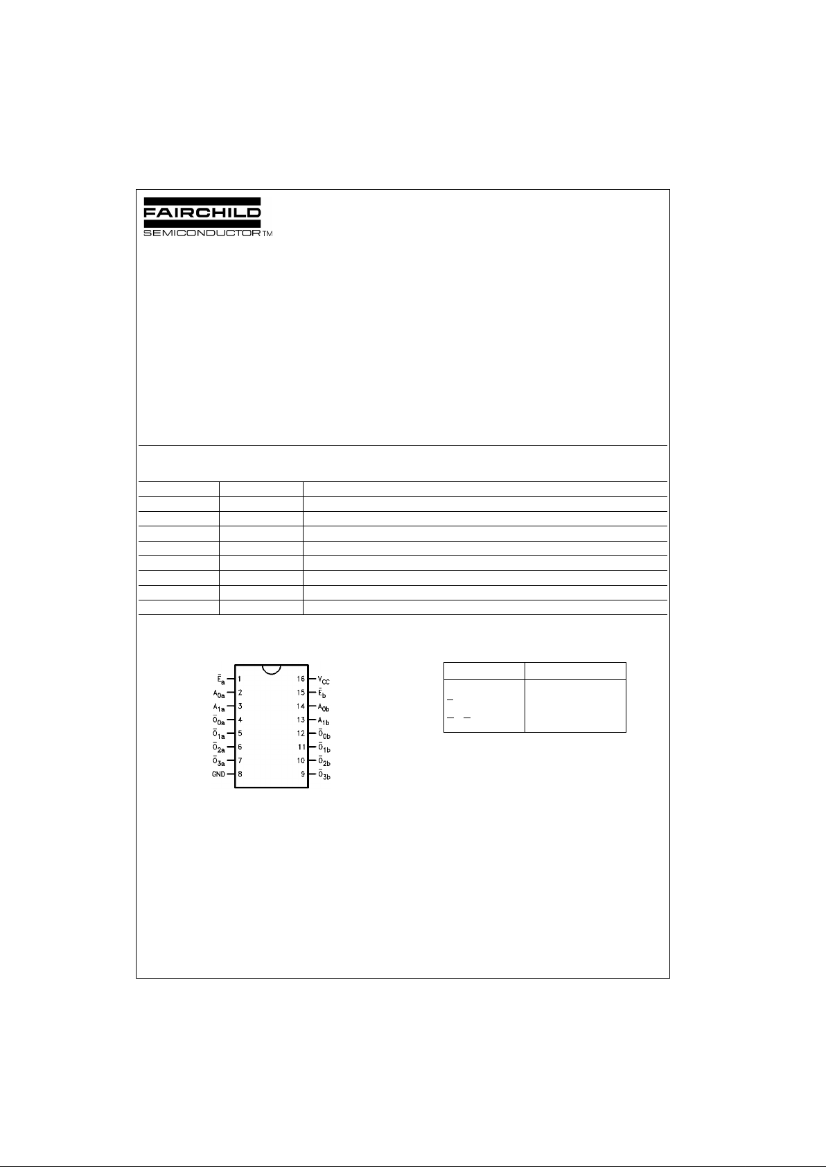
Connection Diagram Pin Descriptions
FACT is a trademark of Fairchild Semiconductor Corporation.
Order Number Package Number Package Description
74AC139SC M16A 16-Lead Small Outline Integrated Circuit (SOIC), JEDEC MS-012, 0.150” Narrow Body
74AC139SJ M16D 16-Lead Small Outline Package (SOIC), EIAJ Type II, 5.3mm Wide
74AC139MTC MTC16 16-Lead Thin Shrink Small Outline Package (TSSOP), JEDEC MO-153, 4.4mm Wide
74AC139PC N16E 16-Lead Plastic Dual-In-Line Package (PDIP), JEDEC MS-001, 0.300” Wide
74ACT139SC M16A 16-Lead Small Outline Integrated Circuit (SOIC), JEDEC MS-012, 0.150” Narrow Body
74ACT139SJ M16D 16-Lead Small Outline Package (SOIC), EIAJ Type II, 5.3mm Wide
74ACT139MTC MTC16 16-Lead Thin Shrink Small Outline Package (TSSOP), JEDEC MO-153, 4.4mm Wide
74ACT139PC N16E 16-Lead Plastic Dual-In-Line Package (PDIP), JEDEC MS-001, 0.300” Wide
Pin Names Description
A
0
, A
1
Address Inputs
E
Enable Inputs
O
0–O3
Outputs
www.fairchildsemi.com 2
74AC139 • 74ACT139
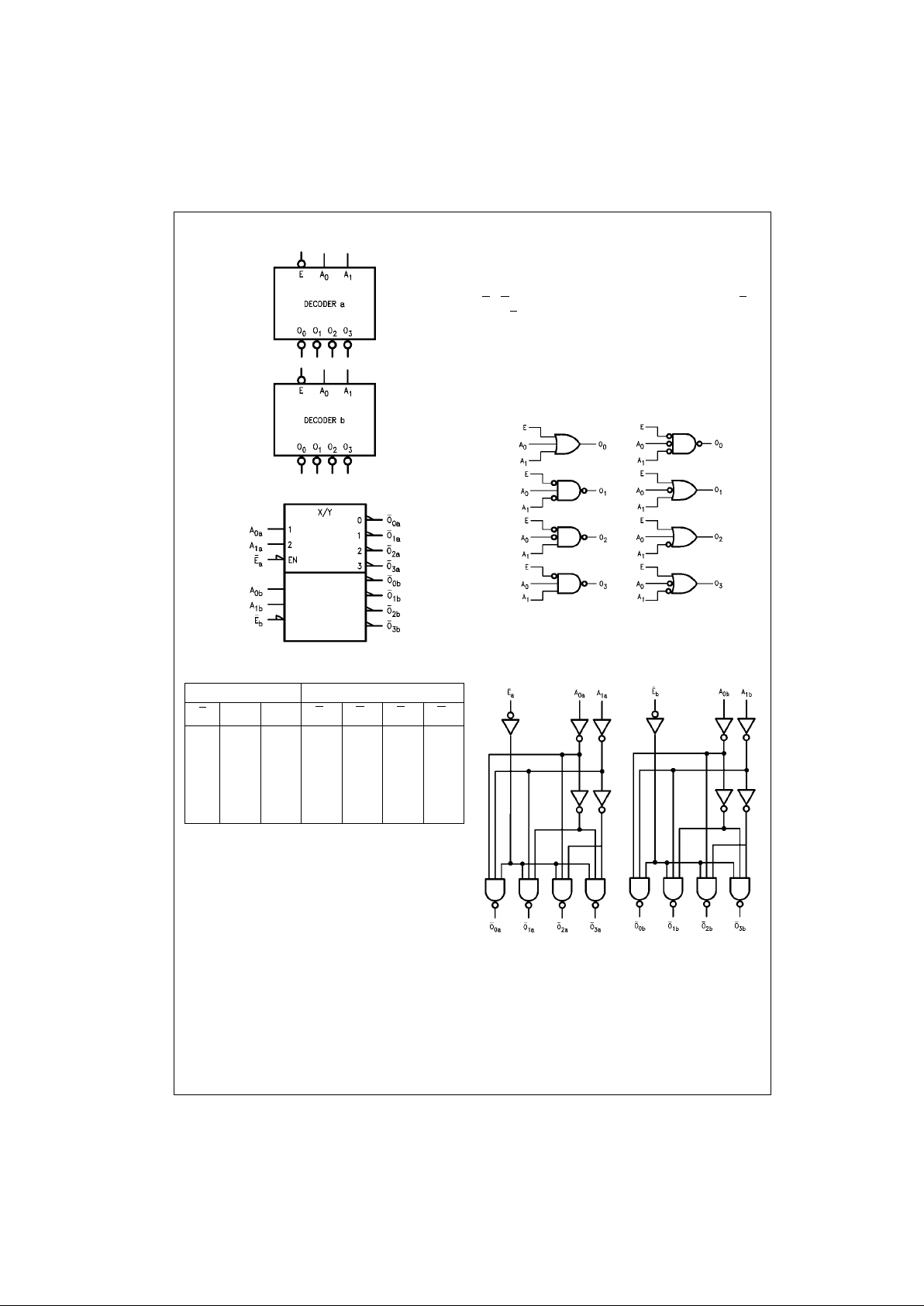
Logic Symbols
IEEE/IEC
Truth Table
H = HIGH Voltage Level
L = LOW Voltage Level
X = Immaterial
Functional Description
The AC/ACT139 is a high-speed dual 1-of-4 decoder/
demultiplexer. The device has two independent de coders,
each of which accepts two binary weighted inputs (A
0–A1
)
and provides four mutually excl usive active-LOW outputs
(O
0–O3
). Each decoder has an active-LOW enable (E).
When E
is HIGH all outputs are forced HIGH. The enable
can be used as the data in put for a 4-o utput dem ultiplexer
application. Each half of the AC/AC T139 gen erates all four
minterms of two variables. The se four mint erms are usefu l
in some applications, re placing multiple gate functi ons as
shown in Figure 1, and thereby reducing the number of
packages required in a logic network.
FIGURE 1. Gate Functions (Each Half)
Logic Diagram
Please note that this diagram is provided only for the understanding of logic
operations and should not be used to estimate propagation delays.
Inputs Outputs
E
A
0
A
1
O
0
O
1
O
2
O
3
HXXHHHH
LLLLHHH
LHLHLHH
LLHHHLH
LHHHHHL
3 www.fairchildsemi.com
74AC139 • 74ACT139
Absolute Maximum Ratings(Note 1) Recommended Operating
Conditions
Note 1: Absolute max imum ratings are those values beyond w hich damage
to the device may occu r. The databook spe cificatio ns shou ld be met, wit hout exception, to ensure that the system de sign is relia ble over its p ower
supply, temperature, and output/input loading variables. Fairchild does not
recommend operation of FACT circuits outside databook specif ic at ions.
DC Electrical Characteristics for AC
Note 2: All outputs loaded; thres holds on input associate d w it h output under test.
Note 3: Maximum test duration 2.0 ms, one output loaded at a time.
Note 4: I
IN
and ICC @ 3.0V are guaranteed to be less than or equa l t o th e respective limit @ 5.5V VCC.
Supply Voltage (VCC) −0.5V to +7.0V
DC Input Diode Current (I
IK
)
V
I
= −0.5V −20 mA
V
I
= VCC + 0.5V +20 mA
DC Input Voltage (V
I
) −0.5V to VCC + 0.5V
DC Output Diode Current (I
OK
)
V
O
= −0.5V −20 mA
V
O
= VCC + 0.5V +20 mA
DC Output Voltage (V
O
) −0.5V to VCC + 0.5V
DC Output S ource
or Sink Current (I
O
) ±50 mA
DC V
CC
or Ground Current
per Output Pin (I
CC
or I
GND
) ±50 mA
Storage Temperature (T
STG
) −65°C to +150°C
Junction Temperature (T
J
)
PDIP 140°C
Supply Voltage (V
CC
)
AC 2.0V to 6.0V
ACT 4.5V to 5.5V
Input Voltage (V
I
)0V to V
CC
Output Voltage (VO)0V to V
CC
Operating Temperature (TA) −40°C to +85°C
Minimum Input Edge Rate (∆V/∆t)
AC Devices
V
IN
from 30% to 70% of V
CC
VCC @ 3.3V, 4.5V, 5.5V 125 mV/ns
Minimum Input Edge Rate (∆V/∆t)
ACT Devices
V
IN
from 0.8V to 2.0V
V
CC
@ 4.5V, 5.5V 125 mV/ns
Symbol Parameter
V
CC
TA = +25°CT
A
= −40°C to +85°C
Units Conditions
(V) Typ Guaranteed Limits
V
IH
Minimum HIGH Level 3.0 1.5 2.1 2.1 V
OUT
= 0.1V
Input Voltage 4.5 2.25 3.15 3.15 V or VCC − 0.1V
5.5 2.75 3.85 3.85
V
IL
Maximum LOW Level 3.0 1.5 0.9 0.9 V
OUT
= 0.1V
Input Voltage 4.5 2.25 1.35 1.35 V or VCC − 0.1V
5.5 2.75 1.65 1.65
V
OH
Minimum HIGH Level 3.0 2.99 2.9 2.9
Output Voltage 4.5 4.49 4.4 4.4 V I
OUT
= −50 µA
5.55.495.4 5.4
VIN = VIL or V
IH
3.0 2.56 2.46 IOH = −12 mA
4.5 3.86 3.76 V I
OH
= −24 mA
5.5 4.86 4.76 I
OH
= −24 mA (Note 2)
V
OL
Maximum LOW Level 3.0 0.002 0.1 0.1
Output Voltage 4.5 0.001 0.1 0.1 V I
OUT
= 50 µA
5.5 0.001 0.1 0.1
VIN = VIL or V
IH
3.0 0.36 0.44 IOL = 12 mA
4.5 0.36 0.44 V IOL = 24 mA
5.5 0.36 0.44 IOL = 24 mA (Note 2)
I
IN
(Note 4)
Maximum Input
Leakage Current
5.5 ± 0.1 ± 1.0 µAVI = VCC, GND
I
OLD
Minimum Dynamic 5.5 75 mA V
OLD
= 1.65V Max
I
OHD
Output Current (Note 3) 5.5 −75 mA V
OHD
= 3.85V Min
I
CC
(Note 4)
Maximum Quiescent
Supply Current
5.5 4.0 40.0 µAVIN = VCC or GND
 Loading...