


April 1993
Revised January 1999
74ABT16652
16-Bit Transceivers and Registers with 3-STATE Outputs
General Description
The ABT16652 consists of sixteen bus transceiver circuits with D-type flip-flops, and control circuitry arranged for multiplexed transmission of data directly from the input bus or from the internal registers. Each byte has separate control inputs which can be shorted together for full 16-bit operation. Data on the A or B bus will be clocked into the registers as the appropriate clock pin goes to HIGH logic level.
Output Enable pins (OEAB, OEBA) are provided to control the transceiver function.
Features
■Independent registers for A and B buses
■Multiplexed real-time and stored data
■Separate control logic for each byte
■A and B output sink capability of 64 mA, source capability of 32 mA
■Guaranteed output skew
■High impedance glitch free bus loading during entire power up and power down cycle
■Nondestructive hot insertion capability
Ordering Code:
Order Number |
Package Number |
Package Description |
|
|
|
74ABT16652CSSC |
MS56A |
56-Lead Shrink Small Outline Package (SSOP), JEDEC MO-118, 0.300” Wide |
|
|
|
74ABT16652CMTD |
MTD56 |
56-Lead Thin Shrink Small Outline Package (TSSOP), JEDEC MO-153, 6.1mm Wide |
|
|
|
Devices also available in Tape and Reel. Specify by appending the suffix letter “X” to the ordering code.
Pin Descriptions |
Connection Diagram |
||||
|
|
|
|
||
|
Pin Names |
Descriptions |
|
||
|
|
|
|
||
|
A0–A16 |
Data Register A Inputs/ |
|
||
|
|
|
|
3-STATE Outputs |
|
|
B0–B16 |
Data Register B Inputs/ |
|
||
|
|
|
|
3-STATE Outputs |
|
|
CPABn, CPBAn |
Clock Pulse Inputs |
|
||
|
SABn, SBAn |
Select Inputs |
|
||
|
OEABn, |
|
n |
Output Enable Inputs |
|
OEBA |
|
||||
Outputs STATE-3 with Registers and Transceivers Bit-16 74ABT16652
© 1999 Fairchild Semiconductor Corporation |
DS011599.prf |
www.fairchildsemi.com |
74ABT16652
Functional Description
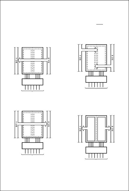
In the transceiver mode, data present at the HIGH impedance port may be stored in either the A or B register or both.
The select (SABn, SBAn) controls can multiplex stored and real-time.
The examples in Figure 1 demonstrate the four fundamental bus-management functions that can be performed with the ABT16652.
Data on the A or B data bus, or both can be stored in the internal D flip-flop by LOW to HIGH transitions at the appropriate Clock Inputs (CPABn, CPBAn) regardless of the Select or Output Enable Inputs. When SAB and SBA are in the real time transfer mode, it is also possible to store data without using the internal D flip-flops by simultaneously enabling OEABn and OEBAn. In this configuration each Output reinforces its Input. Thus when all other data sources to the two sets of bus lines are in a HIGH impedance state, each set of bus lines will remain at its last state.
Note A: Real-Time |
Note C: Storage |
Transfer Bus B to Bus A |
|
|
|
|
|
|
|
|
|
|
|
|
|
|
|
|
|
|
|
OEAB OEBA CPAB CPBA |
SAB |
SBA |
|||
OEAB |
OEBA |
CPAB CPBA SAB |
SBA |
1 |
1 |
1 |
1 |
1 |
1 |
||
1 |
1 |
1 |
1 |
1 |
1 |
X |
H |
X |
X |
X |
|
L |
L |
X |
X |
X |
L |
L |
X |
X |
|
X |
X |
|
|
|
|
|
|
||||||
|
Note B: Real-Time |
|
|
L |
H |
|
|
X |
X |
||
|
|
|
|
|
|
|
|
|
|||
Transfer Bus A to Bus B
Note D: Transfer Storage Data to A or B
|
|
|
|
|
|
|
|
|
|
|
|
|
OEAB OEBA CPAB CPBA SAB |
SBA |
|
|
|
|
|
|
|||||
1 |
1 |
1 |
1 |
1 |
1 |
|
|
|
|
|
|
|
OEAB |
OEBA CPAB1 |
CPBA |
SAB |
SBA |
||||||||
H |
H |
X |
X |
L |
X |
|||||||
1 |
1 |
|
1 |
1 |
1 |
|||||||
|
|
|
|
|
|
|
||||||
|
|
|
|
|
|
H |
L H or L |
H or L |
H |
H |
||
FIGURE 1.
www.fairchildsemi.com |
2 |

Function Table
|
|
|
|
Inputs |
|
|
Inputs/Outputs (Note 1) |
Operating Mode |
||
|
|
|
|
|
|
|
|
|
|
|
OEAB1 |
|
|
1 |
CPAB1 |
CPBA1 |
SAB1 |
SBA1 |
A0 thru A7 |
B0 thru B7 |
|
OEBA |
|
|||||||||
|
|
|
|
|
|
|
|
|
|
|
L |
|
H |
H or L |
H or L |
X |
X |
Input |
Input |
Isolation |
|
|
|
|
|
|
|
|
|
|
|
|
L |
|
H |
|
|
X |
X |
|
|
Store A and B Data |
|
|
|
|
|
|
|
|
|
|
|
|
X |
|
H |
|
H or L |
X |
X |
Input |
Not Specified |
Store A, Hold B |
|
|
|
|
|
|
|
|
|
|
|
|
H |
|
H |
|
|
X |
X |
Input |
Output |
Store A in Both Registers |
|
|
|
|
|
|
|
|
|
|
|
|
L |
|
X |
H or L |
|
X |
X |
Not Specified |
Input |
Hold A, Store B |
|
|
|
|
|
|
|
|
|
|
|
|
L |
|
L |
|
|
X |
X |
Output |
Input |
Store B in Both Registers |
|
|
|
|
|
|
|
|
|
|
|
|
L |
|
L |
X |
X |
X |
L |
Output |
Input |
Real-Time B Data to A Bus |
|
|
|
|
|
|
|
|
|
|
|
|
L |
|
L |
X |
H or L |
X |
H |
|
|
Store B Data to A Bus |
|
|
|
|
|
|
|
|
|
|
|
|
H |
|
H |
X |
X |
L |
X |
Input |
Output |
Real-Time A Data to B Bus |
|
|
|
|
|
|
|
|
|
|
||
H |
|
H |
H or L |
X |
H |
X |
Stored A Data to B Bus |
|||
|
|
|
||||||||
|
|
|
|
|
|
|
|
|
|
|
H |
|
L |
H or L |
H or L |
H |
H |
Output |
Output |
Stored A Data to B Bus and |
|
|
|
|
|
|
|
|
|
|
|
Stored B Data to A Bus |
|
|
|
|
|
|
|
|
|
|
|
H = HIGH Voltage Level
L = LOW Voltage Level X = Immaterial
= LOW to HIGH Clock Transition
Note 1: The data output functions may be enabled or disabled by various signals at OEAB or OEBA inputs. Data input functions are always enabled, i.e., data at the bus pins will be stored on every LOW to HIGH transition on the clock inputs. This also applies to data I/O (A and B: 8–15) and #2 control pins.
Logic Diagrams
Please note that these diagrams are provided only for the understanding of logic operations and should not be used to estimate propagation delays.
74ABT16652
3 |
www.fairchildsemi.com |
 Loading...