


July 1988
Revised August 2000
100350
Low Power Hex D-Type Latch
General Description
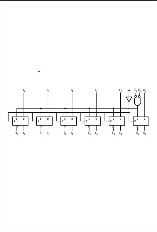
The 100350 contains six D-type latches with true and com- plement outputs, a pair of common Enables (Ea and Eb), and a common Master Reset (MR). A Q output follows its D input when both Ea and Eb are LOW. When either Ea or Eb (or both) are HIGH, a latch stores the last valid data present on its D input before Ea or Eb went HIGH. The MR input overrides all other inputs and makes the Q outputs LOW. All inputs have 50 kΩ pull-down resistors.
Features
■20% power reduction of the 100150
■2000V ESD protection
■Pin/function compatible with 100150
■Voltage compensated operating range = − 4.2V to − 5.7V
Ordering Code:
Order Number |
Package Number |
Package Description |
|
|
|
100350PC |
N24E |
24-Lead Plastic Dual-In-Line Package (PDIP), JEDEC MS-010, 0.400 Wide |
|
|
|
100350QC |
V28A |
28-Lead Plastic Lead Chip Carrier (PLCC), JEDEC MO-047, 0.450 Square |
|
|
|
Devises also available in Tape and Reel. Specify by appending the suffix letter “X” to the ordering code.
Logic Symbol |
Connection Diagrams |
|
24-Pin DIP |
Pin Descriptions
28-Pin PLCC
|
Pin Names |
Description |
||||||
|
|
|
||||||
|
D0–D5 |
Data Inputs |
||||||
|
|
|
|
|
b |
Common Enable Inputs (Active LOW) |
||
|
E |
a, |
E |
|||||
|
MR |
Asynchronous Master Reset Input |
||||||
|
Q0–Q5 |
Data Outputs |
||||||
|
|
|
|
5 |
Complementary Data Outputs |
|||
|
Q |
0–Q |
||||||
Latch Type-D Hex Power Low 100350
© 2000 Fairchild Semiconductor Corporation |
DS009884 |
www.fairchildsemi.com |
100350
Truth Tables
(Each Latch)
Latch Operation
|
|
|
Inputs |
|
Outputs |
|||
|
|
|
|
|
|
|
||
Dn |
Ea |
Eb |
MR |
Qn |
||||
L |
|
L |
|
L |
L |
L |
||
H |
|
L |
|
L |
L |
H |
||
X |
|
H |
|
X |
L |
Latched (Note 1) |
||
X |
|
X |
|
H |
L |
Latched (Note 1) |
||
|
|
|
|
|
|
|
|
|
H = |
HIGH Voltage Level |
L = |
LOW Voltage Level |
X = |
Don’t Care |
Note 1: Retains data present before E positive transition
Asynchronous Operation
|
|
|
Inputs |
|
Outputs |
|||
|
|
|
|
|
|
|
|
|
Dn |
|
Ea |
|
Eb |
MR |
Qn |
||
X |
|
X |
|
X |
H |
L |
||
|
|
|
|
|
|
|
|
|
Logic Diagram
www.fairchildsemi.com |
2 |

Absolute Maximum Ratings(Note 2)
Above which the useful life may be impaired.
Storage Temperature (TSTG) |
− 65° C to + 150° C |
Maximum Junction Temperature (TJ) |
+ 150° C |
VEE Pin Potential to Ground Pin |
− 7.0V to + 0.5V |
Input Voltage (DC) |
VEE to + 0.5V |
Output Current (DC Output HIGH) |
− 50 mA |
ESD (Note 3) |
≥ 2000V |
Recommended Operating
Conditions
Case Temperature (TC) |
0° C to + 85° C |
Supply Voltage (VEE) |
− 5.7V to − 4.2V |
Note 2: The “Absolute Maximum Ratings” are those values beyond which the safety of the device cannot be guaranteed. The device should not be operated at these limits. The parametric values defined in the Electrical Characteristics tables are not guaranteed at the absolute maximum rating. The “Recommended Operating Conditions” table will define the conditions for actual device operation.
Note 3: ESD testing conforms to MIL-STD-883, Method 3015.
DC Electrical Characteristics |
(Note 4) |
|
|
|
|
|
|
||||||||
VEE = − 4.5V to − 5.7V, VCC = VCCA = |
GND, TC = 0° C to + 85° C |
|
|
|
|
|
|
||||||||
Symbol |
Parameter |
|
|
|
|
|
|
Min |
Typ |
Max |
Units |
|
Conditions |
|
|
|
|
|
|
|
|
|
|
|
|
|
|
|
|
|
|
VOH |
Output HIGH Voltage |
|
|
|
|
|
− |
1025 |
− 955 |
− 870 |
mV |
VIN = |
VIH (Max) |
Loading with |
|
VOL |
Output LOW Voltage |
|
|
|
|
|
− |
1830 |
− 1705 |
− 1620 |
or VIL (Min) |
50Ω to − |
2.0V |
||
|
|
|
|
|
|
||||||||||
VOHC |
Output HIGH Voltage |
|
|
|
|
|
− |
1035 |
|
|
mV |
VIN = |
VIH (Min) |
Loading with |
|
VOLC |
Output LOW Voltage |
|
|
|
|
|
|
|
|
− 1610 |
or VIL (Max) |
50Ω to − |
2.0V |
||
|
|
|
|
|
|
|
|
|
|||||||
VIH |
Input HIGH Voltage |
|
|
|
|
|
− |
1165 |
|
− 870 |
mV |
Guaranteed HIGH Signal for All Inputs |
|
||
VIL |
Input LOW Voltage |
|
|
|
|
|
− |
1830 |
|
− 1475 |
mV |
Guaranteed LOW Signal for All Inputs |
|
||
IIL |
Input LOW Current |
|
|
|
|
|
|
0.50 |
|
|
µ A |
VIN = |
VIL (Min) |
|
|
IIH |
Input HIGH Current |
|
|
MR |
|
|
|
240 |
|
|
|
|
|
||
|
|
|
|
Dn |
|
|
|
240 |
µ A |
VIN = |
VIH (Max) |
|
|
||
|
|
|
E |
a, |
E |
b |
|
|
|
240 |
|
|
|
|
|
IEE |
Power Supply |
|
|
|
|
|
|
|
|
|
|
Inputs Open |
|
|
|
|
Current |
|
|
|
|
|
|
− 89 |
|
− 44 |
mA |
VEE = |
− 4.2V to − 4.8V |
|
|
|
|
|
|
|
|
|
|
− 93 |
|
− 44 |
|
VEE = |
− 4.2V to − 5.7V |
|
|
Note 4: The specified limits represent the “worst case” value for the parameter. Since these values normally occur at the temperature extremes, additional noise immunity and guard banding can be achieved by decreasing the allowable system operating ranges. Conditions for testing shown in the tables are chosen to guarantee operation under “worst case” conditions.
DIP AC Electrical Characteristics
VEE = − 4.2V to − 5.7V, VCC = VCCA = |
GND |
|
|
|
|
|
|
|
||||||
Symbol |
|
|
|
|
Parameter |
|
TC = 0° C |
TC = + 25° C |
TC = + 85° C |
Units |
Conditions |
|||
|
|
|
|
|
|
|
Min |
Max |
Min |
Max |
Min |
Max |
|
|
|
|
|
|
|
|
|
|
|
|
|
||||
tPLH |
Propagation Delay |
|
|
|
|
|
|
|
|
|
||||
tPHL |
Dn to Output |
|
0.50 |
1.40 |
0.50 |
1.40 |
0.50 |
1.50 |
ns |
|
||||
|
(Transparent Mode) |
|
|
|
|
|
|
|
|
Figures 1, 2 |
||||
|
|
|
|
|
|
|
|
|
|
|
||||
tPLH |
Propagation Delay |
|
0.75 |
1.85 |
0.75 |
1.85 |
0.75 |
2.05 |
ns |
|
||||
|
|
|
|
|
|
|
|
|||||||
tPHL |
Ea, Eb to Output |
|
||||||||||||
|
|
|
|
|
|
|
|
|
||||||
tPLH |
Propagation Delay |
|
0.90 |
2.10 |
0.90 |
2.10 |
0.90 |
2.10 |
ns |
Figures 1, 3 |
||||
tPHL |
MR to Output |
|
||||||||||||
|
|
|
|
|
|
|
|
|
||||||
tTLH |
Transition Time |
|
0.35 |
1.30 |
0.35 |
1.30 |
0.35 |
1.30 |
ns |
Figures 1, 2 |
||||
tTHL |
20% to 80%, 80% to 20% |
|
||||||||||||
|
|
|
|
|
|
|
|
|
||||||
tS |
Setup Time |
|
|
|
|
|
|
|
|
|
||||
|
D0–D5 |
|
1.00 |
|
1.00 |
|
1.00 |
|
ns |
Figures 3, 4 |
||||
|
MR (Release Time) |
|
1.60 |
|
1.60 |
|
1.60 |
|
|
|
||||
|
|
|
|
|
|
|
|
|
|
|
||||
tH |
Hold Time, D0–D5 |
|
0.40 |
|
0.40 |
|
0.40 |
|
ns |
Figure 4 |
||||
tPW(L) |
Pulse Width LOW |
|
2.00 |
|
2.00 |
|
2.00 |
|
ns |
Figure 2 |
||||
|
|
|
|
|
|
|
|
|
|
|||||
|
Ea, Eb |
|
|
|
|
|
|
|
|
|
||||
tPW(H) |
Pulse Width HIGH, MR |
|
2.00 |
|
2.00 |
|
2.00 |
|
ns |
Figure 3 |
||||
100350
3 |
www.fairchildsemi.com |
 Loading...