


74ABT241CCW
Fairchild Semiconductor 74ABT241CCW, 74ABT241CSJX, 74ABT241CSJ, 74ABT241CSCX, 74ABT241CSC Datasheet
...
© 1999 Fairchild Semiconductor Corporation DS011691 www.fairchildsemi.com
January 1995
Revised November 1999
74ABT241 Octal Buffer/Line Driver with 3-STATE Outputs
74ABT241
Octal Buffer/Line Driv e r wit h 3- S TATE Outputs
General Description
The ABT241 is an octal buffer and line driver with 3-STATE
outputs designed to be employed as a memory and
address driver, clock driver, or bus-oriented transmitter/
receiver.
Features
■ Non-inverting buffers
■ Output sink capability of 64 mA, source capability of
32 mA
■ Guarante ed latchup protection
■ High impedance glitch free bus loading during entire
power up and power down cycle
■ Nondestructive hot insertion capability
Ordering Code:
Device also available in Tape and Reel. Specify by appending the suffix letter “X” to the ordering code.
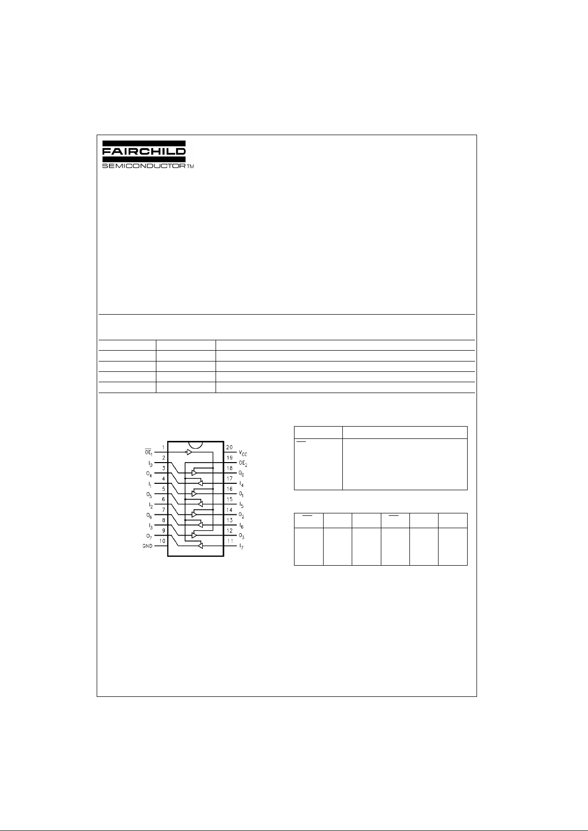
Connection Diagram Pin Descriptions
Truth Table
H = HIGH Voltage Level
L = LOW Voltage Level
X = Immaterial
Z = High Impedance
Order Number Package Number Package Description
74ABT241CSC M20B 20-Lead Small Outline Integrated Circuit (SOIC), JEDEC MS-013, 0.300” Wide Body
74ABT241CSJ M20D 20-Lead Small Outline Package (SOP), EIAJ TYPE II, 5.3mm Wide
74ABT241CMSA MSA20 20-Lead Shrink Small Outline Package (SSOP), EIAJ TYPE II, 5.3mm Wide
74ABT241CMTC MTC20 20-Lead Thin Shrink Small Outline Package (TSSOP), JEDEC MO-153, 4.4mm Wide
Pin Names Description
OE
1
Output Enable Input (Active LOW)
OE
2
Output Enable Input (Active HIGH)
I
0–I7
Inputs
O
0–O7
Outputs
OE
1I0–3
O
0–3
OE
2I4–7
O
4–7
HXZLXZ
LHHHHH
LLLHLL
www.fairchildsemi.com 2
74ABT241
Absolute Maximum Ratings(Note 1) Recommended Operating
Conditions
Note 1: Absolute maximum ratings are values beyond which the device
may be damaged or have its useful life impaired. Functional operation
under these conditi ons is not implied.
Note 2: Either voltage lim it or c urrent limit is sufficient to prot ect inputs.
DC Electrical Characteristics
Note 3: For 8 bits toggling, I
CCD
< 0.8 mA/MHz.
Note 4: Guaranteed, but not tested.
Storage Temperature −65°C to +150°C
Ambient Temperature under Bias −55°C to +125°C
Junction Temperature under Bias −55°C to +150°C
V
CC
Pin Potential to Ground Pin −0.5V to +7.0V
Input Voltage (Note 2) −0.5V to +7.0V
Input Current (Note 2) −30 mA to +5.0 mA
Voltage Applied to Any Output
in the Disabled or
Power-Off State −0.5V to 5.5V
in the HIGH State −0.5V to V
CC
Current Applied to Output
in LOW State (Max) twice the rated I
OL
(mA)
DC Latchup Source Current
(Over Comm Operating Rang e) −500 mA
Over Voltage Latchup (I/O) 10V
Free Air Ambient Temperature −40°C to +85°C
Supply Voltage +4.5V to +5.5V
Minimum Input Edge Rate (∆V/∆t)
Data Input 50 mV/ns
Enable Input 20 mV/ns
Symbol Parameter Min Typ Max Units
V
CC
Conditions
V
IH
Input HIGH Voltage 2.0 V Recognized HIGH Signal
V
IL
Input LOW Voltage 0.8 V Recognized LOW Signal
V
CD
Input Clamp Diode Voltage −1.2 V Min IIN = −18 mA
V
OH
Output HIGH Voltage 2.5 V Min IOH = −3 mA
2.0 V Min IOH = −32 mA
V
OL
Output LOW Voltage 0.55 V Min IOL = 64 mA
I
IH
Input HIGH Current 1
µAMax
VIN = 2.7V (Note 4)
1V
IN
= V
CC
I
BVI
Input HIGH Current Breakdown Test 7 µAMaxVIN = 7.0V
I
IL
Input LOW Current −1
µAMax
VIN = 0.5V (Note 4)
−1V
IN
= 0.0V
V
ID
Input Leakage Test 4.75 V 0.0 IID = 1.9 µA
All Other Pins Grounded
I
OZH
Output Leakage Current 10 µA0 − 5.5V
V
OUT
= 2.7V; OEn = 2.0V
I
OZL
Output Leakage Current −10 µA0 − 5.5V
V
OUT
= 0.5V; OEn = 2.0V
I
OS
Output Short-Circuit Current −100 −275 mA Max V
OUT
= 0.0V
I
CEX
Output High Leakage Current 50 µAMaxV
OUT
= V
CC
I
ZZ
Bus Drainage Test 100 µA0.0V
OUT
= 5.5V; All Others GND
I
CCH
Power Supply Current 50 µA Max All Outputs HIGH
I
CCL
Power Supply Current 30 mA Max All Outputs LOW
I
CCZ
Power Supply Current
50 µAMax
OEn = VCC;
All Others at VCC or Ground
I
CCT
Additional ICC/Input Outputs Enabled 2.5 mA
Max
VI = VCC − 2.1V
Outputs 3-STATE 2.5 mA Enable Input VI = VCC − 2.1V
Outputs 3-STATE 50 µA Data Input VI = VCC − 2.1V
All Others at VCC or Ground
I
CCD
Dynamic I
CC
No Load mA/
Max
Outputs Open
(Note 4) 0.1
MHz
OEn = GND, (Note 3)
One Bit Toggling, 50%
Duty Cycle
3 www.fairchildsemi.com
74ABT241
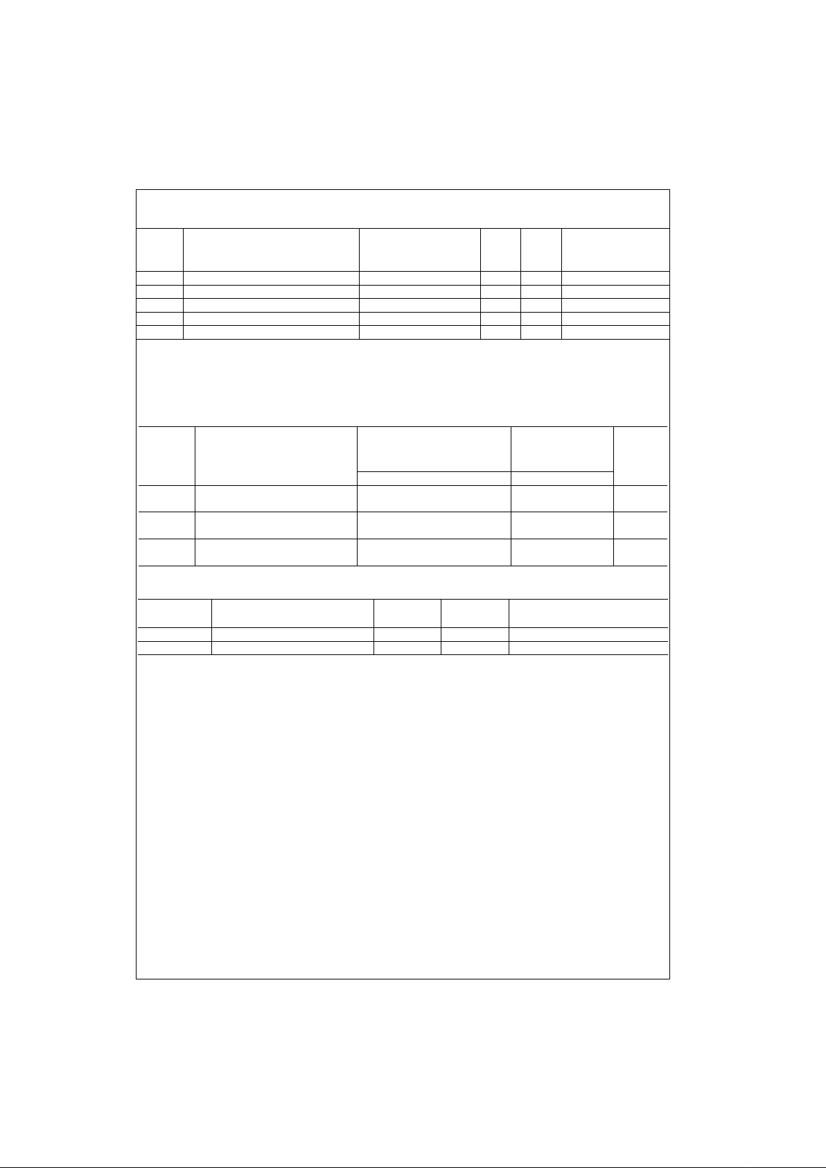
DC Electrical Characteristics
(SOIC package)
Note 5: Max number of outputs defined as (n). n − 1 data inputs are driven 0V to 3V. One output at LOW. Guaranteed, but not test ed.
Note 6: Max number of data inputs (n) s witc hing. n − 1 inputs switching 0V to 3V. Input-under-test switching: 3V to threshold (V
ILD
), 0V to threshold (V
IHD
).
Guaranteed, but not tested.
Note 7: Max number of outputs defined as (n). n − 1 data inputs are driven 0V to 3V. One output HI GH . Guaranteed, but not te s t ed.
AC Electrical Characteristics
(SOIC and SSOP package)
Capacitance
Note 8: C
OUT
is measured at frequency f = 1 MHz, per MIL-STD-883, Method 3012.
Conditions
Symbol Parameter Min Typ Max Units
V
CC
CL = 50 pF,
R
L
= 500Ω
V
OLP
Quiet Output Maximum Dynamic V
OL
0.5 0.8 V 5.0 TA = 25°C (Note 5)
V
OLV
Quiet Output Minimum Dynamic V
OL
−1.3 −0.8 V 5.0 TA = 25°C (Note 5)
V
OHV
Minimum HIGH Level Dynamic Output Voltage 2.7 3.1 V 5.0 TA = 25°C (Note 7)
V
IHD
Minimum HIGH Level Dynamic Input Voltage 2.0 1.5 V 5.0 TA = 25°C (Note 6)
V
ILD
Maximum LOW Level Dynamic Input Voltage 1.1 0.8 V 5.0 TA = 25°C (Note 6)
TA = +25°CT
A
= −40°C to +85°C
VCC = +5V VCC = 4.5V–5.5V
Symbol Parameter
CL = 50 pF CL = 50 pF
Units
Min Typ Max Min Max
t
PLH
Propagation Delay 1.0 4.6 1.0 4.6
ns
t
PHL
Data to Outputs 1.0 4.6 1.0 4.6
t
PZH
Output Enable 1.1 6.8 1.1 6.8
ns
t
PZL
Time 1.3 6 .8 1.3 6.8
t
PHZ
Output Disable 1.6 6.8 1.6 6.8
ns
t
PLZ
Time 1.0 5 .9 1.0 5.9
Symbol Parameter Typ Units
Conditions
T
A
= 25°C
C
IN
Input Capacitance 5.0 pF VCC = 0V
C
OUT
(Note 8) Output Capacitance 9.0 pF VCC = 5.0V
 Loading...