


February 1992
Revised August 2000
100398
Quad Differential ECL/TTL Translating Transceiver with Latch
General Description
The 100398 is a quad latched transceiver designed to convert TTL logic levels to differential F100K ECL logic levels and vice versa. This device was designed with the capability of driving a differential 25Ω ECL load with cutoff capability, and will sink a 64 mA TTL load. The 100398 is ideal for mixed technology applications utilizing either an ECL or TTL backplane.
The direction of translation is set by the direction control pin (DIR). The DIR pin on the 100398 accepts TTL logic levels. A TTL LOW on DIR sets up the ECL pins as inputs and TTL pins as outputs. A TTL HIGH on DIR sets up the TTL pins as inputs and ECL pins as outputs.
A LOW on the output enable input pin (OE) holds the ECL output in a cut-off state and the TTL outputs at a high impedance level. A HIGH on the latch enable input (LE) latches the data at both inputs even though only one output is enabled at the time. A LOW on LE makes the latch transparent.
The cut-off state is designed to be more negative than a normal ECL LOW level. This allows the output emitter-fol- lowers to turn off when the termination supply is − 2.0V, presenting a high impedance to the data bus. This high impedance reduces termination power and prevents loss of low state noise margin when several loads share the bus.
The 100398 is designed with FAST TTL output buffers, featuring optimal DC drive and capable of quickly charging and discharging highly capacitive loads. All Inputs have 50 kΩ pull-down resistors.
Features
■Differential ECL input/output structure
■64 mA FAST TTL outputs
■25Ω differential ECL outputs with cut-off
■Bi-directional translation
■2000V ESD protection
■Latched outputs
■3-STATE outputs
■Voltage compensated operating range = − 4.2V to − 5.7V
Ordering Code:
Order Number |
Package Number |
Package Description |
|
|
|
100398PC |
N24E |
24-Lead Plastic Dual-In-Line Package (PDIP), JEDEC MS-010, 0.400 Wide |
|
|
|
100398QC |
V28A |
28-Lead Plastic Lead Chip Carrier (PLCC), JEDEC MO-047, 0.450 Square |
|
|
|
100398QI |
V28A |
28-Lead Plastic Lead Chip Carrier (PLCC), JEDEC MO-047, 0.450 Square |
|
|
Industrial Temperature Range (− 40° C to + 85° C) |
|
|
|
Devices also available in Tape and Reel. Specify by appending the suffix letter “X” to the ordering code.
FAST is a registered trademark of Fairchild Semiconductor.
Latch with Transceiver Translating ECL/TTL Differential Quad 100398
© 2000 Fairchild Semiconductor Corporation |
DS010970 |
www.fairchildsemi.com |
100398
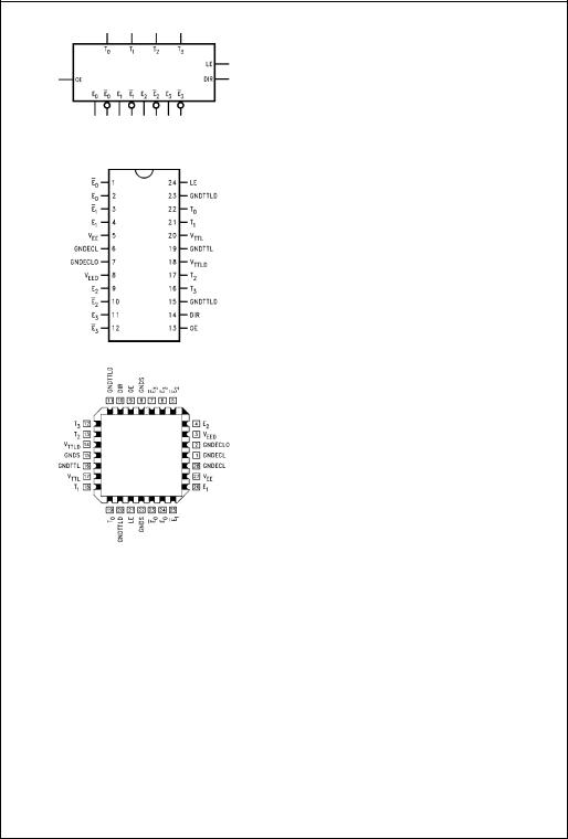
Logic Symbol
Connection Diagrams
24-Pin DIP
28-Pin PLCC
Pin Descriptions
|
Pin Names |
Description |
|
|
|
|
E0–E3 |
ECL Data I/O |
|
E0–E3 |
Complementary ECL |
|
|
Data I/O |
|
T0–T3 |
TTL Data I/O |
|
OE |
Output Enable Input Levels |
|
LE |
Latch Enable Input Levels |
|
DIR |
Direction Control |
|
|
Input (TTL levels) |
|
|
|
|
GNDECL |
ECL Ground |
|
GNDECLO |
ECL Output Ground |
|
GNDS |
ECL Ground-to-Substrate |
|
VEE |
ECL Quiescent Power Supply |
|
VEED |
ECL Dynamic Power Supply |
|
GNDTTL |
TTL Quiescent Ground |
|
GNDTTLD |
TTL Dynamic Ground |
|
VTTL |
TTL Quiescent Power Supply |
|
VTTLD |
TTL Dynamic Power Supply |
Truth Table |
|
|
|
|
LE |
DIR |
|
OE |
ECL |
TTL |
Notes |
|
|
|
|
|
|
Port |
Port |
|
|
|
|
|
|
|
|
||
|
|
|
|
|
|
|
|
|
|
|
0 |
0 |
|
0 |
LOW |
Z |
|
|
|
|
|
|
|
(Cut-Off) |
|
|
|
|
|
|
|
|
|
|
|
|
|
0 |
0 |
|
1 |
Input |
Output |
(Note 1)(Note 4) |
|
|
|
|
|
|
|
|
|
|
|
0 |
1 |
|
0 |
LOW |
Z |
|
|
|
|
|
|
|
(Cut-Off) |
|
|
|
|
|
|
|
|
|
|
|
|
|
0 |
1 |
|
1 |
Output |
Input |
(Note 2)(Note 4) |
|
|
|
|
|
|
|
|
|
|
|
1 |
0 |
|
0 |
Input |
Z |
(Note 1)(Note 3) |
|
|
|
|
|
|
|
|
|
|
|
1 |
0 |
|
1 |
Latched |
X |
(Note 1)(Note 3) |
|
|
|
|
|
|
|
|
|
|
|
1 |
1 |
|
0 |
Low |
Input |
(Note 2)(Note 3) |
|
|
|
|
|
|
(Cut-Off) |
|
|
|
|
|
|
|
|
|
|
|
|
|
1 |
1 |
|
1 |
Latched |
X |
(Note 2)(Note 3) |
|
|
|
|
|
|
|
|
|
|
H = |
HIGH Voltage Level |
|
|
|
|||
L = |
LOW Voltage Level |
|
|
|
|
|||
X = |
Don’t Care |
|
|
|
|
|||
Z = |
High Impedance |
|
|
|
|
|||
Note 1: ECL input to TTL output mode.
Note 2: TTL input to ECL output mode.
Note 3: Retains data present before LE set HIGH.
Note 4: Latch is transparent.
www.fairchildsemi.com |
2 |

Functional Diagram |
Detail |
Note: LE, and OE use TTL logic levels
100398
3 |
www.fairchildsemi.com |

100398
Absolute Maximum Ratings(Note 5)
Storage Temperature (TSTG) |
− 65° C to + 150° C |
Maximum Junction Temperature |
|
(TJ) |
+ 150° C |
VEE Pin Potential to Ground Pin |
− 7.0V to + 0.5V |
VTTL Pin Potential to Ground Pin |
− 0.5V to + 6.0V |
ECL Input Voltage (DC) |
VEE to + 0.5V |
ECL Output Current |
|
(DC Output HIGH) |
− 50 mA |
TTL Input Voltage (Note 6) |
− 0.5V to + 7.0V |
TTL Input Current (Note 6) |
− 30 mA to + 5.0 mA |
Voltage Applied to Output in |
|
HIGH State 3-STATE Output |
− 0.5V to + 5.5V |
Current Applied to TTL |
|
Output in LOW State (Max) |
twice the Rated IOL (mA) |
ESD (Note 7) |
≥ 2000V |
Recommended Operating
Conditions
Case Temperature (TC) |
|
Commercial |
0° C to + 85° C |
Industrial |
− 40° C to + 85° C |
ECL Supply Voltage (VEE) |
− 5.7V to − 4.2V |
TTL Supply Voltage (VTTL) |
+ 4.5V to + 5.5V |
Note 5: The “Absolute Maximum Ratings” are those values beyond which the safety of the device cannot be guaranteed. The device should not be operated at these limits. The parametric values defined in the Electrical Characteristics tables are not guaranteed at the absolute maximum rating. The “Recommended Operating Conditions” table will define the conditions for actual device operation.
Note 6: The specified limits represent the “worst case” value for the parameter. Since these values normally occur at the temperature extremes, additional noise immunity and guardbanding can be achieved by decreasing the allowable system operating ranges. Conditions for testing shown in the tables are chosen to guarantee operation under “worst case” conditions.
Note 7: ESD testing conforms to MIL-STD-883, Method 3015.
Commercial Version
TTL-to-ECL DC Electrical Characteristics (Note 9)
VEE = − 4.2V to − 5.7V, GND = 0V, TC = |
0° C to + 85° C, VTTL = |
+ 4.5V to + 5.5V |
|
|
|
||||||
Symbol |
Parameter |
|
Min |
|
Typ |
Max |
Units |
|
Conditions |
||
|
|
|
|
|
|
|
|
|
|
|
|
VOH |
Output HIGH Voltage |
|
− 1025 |
|
− 955 |
− 870 |
mV |
VIN = |
VIH(Max) or VIL(Min) |
||
VOL |
Output LOW Voltage |
|
− 1830 |
|
− 1705 |
− 1620 |
mV |
Loading with 50Ω to − 2V |
|||
|
|
Cutoff Voltage |
|
|
|
|
− 2000 |
− 1950 |
mV |
OE and LE LOW, DIR HIGH |
|
|
|
|
|
|
|
|
|
|
|
VIN = |
VIH(Max) or VIL(Min), |
|
|
|
|
|
|
|
|
|
|
Loading with 50Ω to − 2V |
|
|
|
|
|
|
|
|
|
|
|
|
|
VOHC |
Output HIGH Voltage |
|
− 1035 |
|
|
|
mV |
|
|
||
|
|
Corner Point High |
|
|
|
|
VIN = |
VIH(Min) or VIL(Max) |
|||
|
|
|
|
|
|
|
|
|
|||
VOLC |
Output LOW Voltage |
|
|
|
|
|
− 1610 |
mV |
Loading with 50Ω to − 2V |
||
|
|
Corner Point Low |
|
|
|
|
|
|
|
||
|
|
|
|
|
|
|
|
|
|
|
|
|
|
|
|
|
|
|
|
|
|||
VIH |
Input HIGH Voltage |
|
2.0 |
|
|
5.0 |
V |
Over VTTL, VEE, TC Range |
|||
VIL |
Input LOW Voltage |
|
|
0 |
|
|
0.8 |
V |
Over VTTL, VEE, TC Range |
||
IIH |
Input HIGH Current |
|
|
|
|
|
5.0 |
µ A |
VIN = |
+ 2.7V |
|
|
|
Breakdown Test |
|
|
|
|
|
0.5 |
mA |
VIN = |
+ 5.5V |
IIL |
Input LOW Current |
|
− |
700 |
|
|
|
µ A |
VIN = |
+ 0.5V |
|
VFCD |
Input Clamp |
|
− |
1.2 |
|
|
|
V |
IIN = |
− 18 mA |
|
|
|
Diode Voltage |
|
|
|
|
|||||
|
|
|
|
|
|
|
|
|
|
|
|
|
|
|
|
|
|
|
|
|
|
||
IEE |
VEE Supply Current |
|
− |
99 |
|
|
− 50 |
mA |
LE LOW, OE and DIR HIGH |
||
|
|
|
|
|
|
|
|
|
|
Inputs Open |
|
|
|
|
|
|
|
|
|
|
|
||
IEEZ |
VEE Supply Current |
|
− |
159 |
|
|
− 90 |
mA |
LE and OE LOW, DIR HIGH |
||
|
|
|
|
|
|
|
|
|
|
Inputs Open |
|
|
|
|
|
|
|
|
|
|
|
|
|
Note 8: Either voltage limit or current limit is sufficient to protect inputs.
Note 9: The specified limits represent the “worst case” value for the parameter. Since these values normally occur at the temperature extremes, additional noise immunity and guardbanding can be achieved by decreasing the allowable system operating ranges. Conditions for testing shown in the tables are chosen to guarantee operation under “worst case” conditions.
www.fairchildsemi.com |
4 |
 Loading...