


74AC109SJX
Fairchild Semiconductor 74AC109SJX, 74AC109SJ, 74AC109SCX, 74AC109SC, 74AC109PC Datasheet
...
© 2000 Fairchild Semiconductor Corporation DS009923 www.fairchildsemi.com
November 1988
Revised August 2000
74AC109 • 74ACT109 Dual JK Positive Edge-Triggered Flip-Flop
74AC109 • 74ACT109
Dual JK
Positive Edge-Triggered Flip-Flop
General Description
The AC/ACT109 consists of two high-speed completely
independent transition clocked JK
flip-flops. The clocking
operation is independe nt of rise and fall times of the cl ock
waveform. The JK
design allows operation as a D-Type
flip-flop (refer to AC/ACT74 data sheet) by connecting the J
and K
inputs together.
Asynchronous Inputs:
LOW input to S
D
(Set) sets Q to HIGH level
LOW input to C
D
(Clear) sets Q to LOW level
Clear and Set are independent of clock
Simultaneous LOW on C
D
and SD makes
both Q and Q HIGH
Features
■ ICC reduced by 50%
■ Outputs source/sink 24 mA
■ ACT109 has TTL-compatible inputs
Ordering Code:
Device also available in Tape and Reel. Specify by appending s uffix let te r “X” to the ordering code.
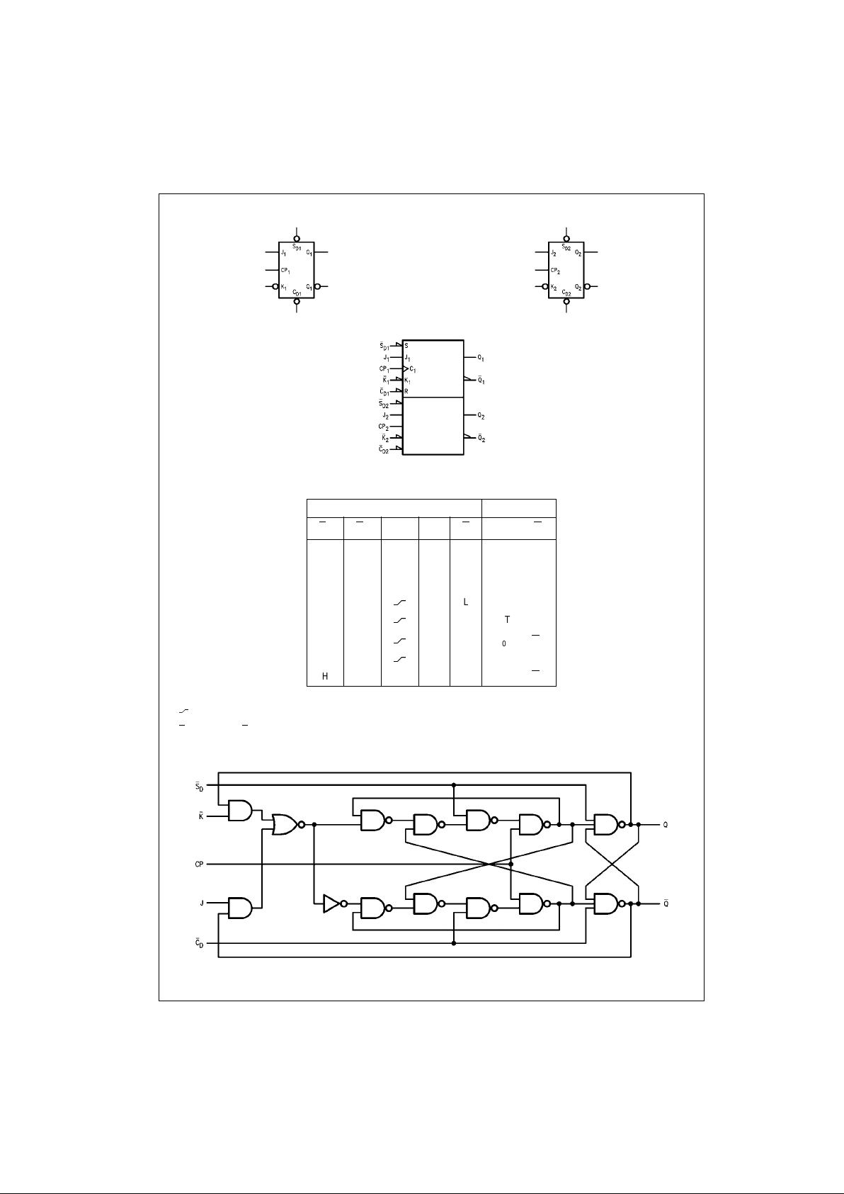
Connection Diagram Pin Descriptions
FACT is a trademark of Fairchild Semiconductor Corporation.
Order Number Package Number Package Description
74AC109SC M16A 16-Lead Small Outline Integrated Circuit (SOIC), JEDEC MS-012, 0.150 Narrow
74AC109SJ M16D 16-Lead Small Outline Package (SOP), EIAJ TYPE II, 5.3mm Wide
74AC109MTC MTC16 16-Lead Thin Shrink Small Outline Package (TSSOP), JEDEC MO-153, 4.4mm Wide
74AC109PC N16E 16-Lead Plastic Dual-in-Line Package (PDIP), JEDEC MS-001, 0.300” Wide
74ACT109SC M16A 16-Lead Small Outline Integrated Circuit (SOIC), JEDEC MS-012, 0.150 Narrow
74AC109MTC MTC16 16-Lead Thin Shrink Small Outline Package (TSSOP), JEDEC MO-153, 4.4mm Wide
74ACT109PC N16E 16-Lead Plastic Dual-In-Line Package (PDIP), JEDEC MS-001, 0.300 Wide
Pin Names Description
J
1
, J2, K1, K
2
Data Inputs
CP
1
, CP
2
Clock Pulse Inputs
C
D1
, C
D2
Direct Clear Inputs
S
D1
, S
D2
Direct Set Inputs
Q
1
, Q2, Q1, Q2Outputs
www.fairchildsemi.com 2
74AC109 • 74ACT109
Logic Symbols
IEEE/IEC
Truth Table
(each half)
H = HIGH Voltage Level
L = LOW Voltage Level
= LOW-to-HIGH Transition
X = Immaterial
Q
0(Q0
) = Previous Q0(Q0) before LOW-to-HIGH Transition of Clock
Logic Diagram (one half shown)
Please note that this diagram is provided only for the understanding of logic operations and should not be used to estimate propagation delays.
Inputs Outputs
S
D
C
D
CP J K QQ
LHXXXHL
HLXXXLH
LLXXXHH
HH
LL L H
HH
HL Toggle
HH
LHQ0Q
0
HH
HH H L
HHLXXQ
0
Q
0
3 www.fairchildsemi.com
74AC109 • 74ACT109
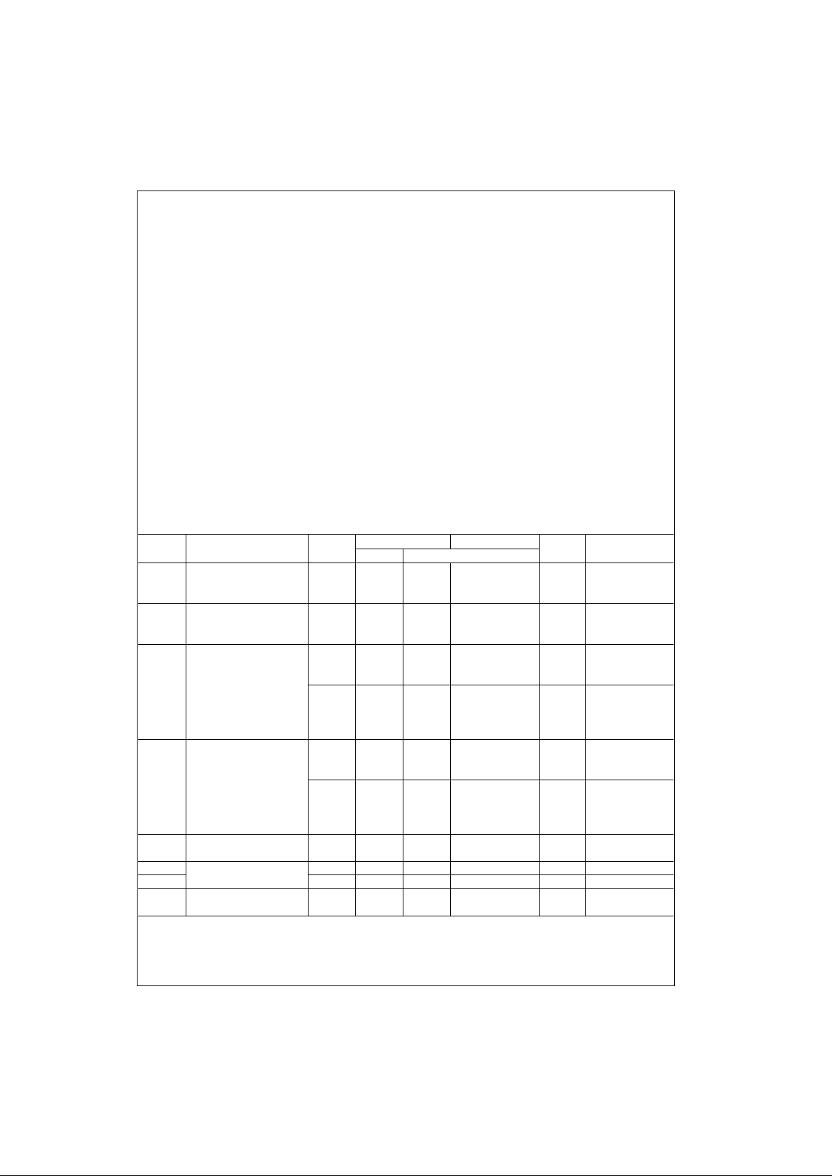
Absolute Maximum Ratings(Note 1) Recommended Operating
Conditions
Note 1: Absolute max imum ratings are those values beyond w hich damage
to the device may occu r. The databook spe cificatio ns shou ld be met, wit hout exception, to ensure that the system de sign is relia ble over its p ower
supply, temperature, and output/input loading variables.Fairchild does not
recommend operation of FACT circuits outside databook specif ic at ions.
DC Electrical Characteristics for AC
Note 2: All outputs loaded; thres holds on input associate d w it h output under test.
Note 3: Maximum test duration 2.0 ms, one output loaded at a time.
Note 4: I
IN
and ICC @ 3.0V are guaranteed to be less than or equa l t o th e respective limit @ 5.5V VCC.
Supply Voltage (VCC) −0.5V to +7.0V
DC Input Diode Current (I
IK
)
V
I
= −0.5V −20 mA
V
I
= VCC + 0.5V +20 mA
DC Input Voltage (V
I
) −0.5V to VCC + 0.5V
DC Output Diode Current (I
OK
)
V
O
= −0.5V −20 mA
V
O
= VCC + 0.5V +20 mA
DC Output Voltage (V
O
) −0.5V to VCC + 0.5V
DC Output S ource
or Sink Current (I
O
) ± 50 mA
DC V
CC
or Ground Current
per Output Pin (I
CC
or I
GND
) ± 50 mA
Storage Temperature (T
STG
) −65°C to +150°C
Junction Temperature (T
J
)
PDIP 140
°C
Supply Voltage (V
CC
)
AC 2.0V to 6.0V
ACT 4.5V to 5.5V
Input Voltage (V
I
)0V to V
CC
Output Voltage (VO)0V to V
CC
Operating Temperature (TA) −40°C to +85°C
Minimum Input Edge Rate (
∆V/∆t)
AC Devices
V
IN
from 30% to 70% of V
CC
VCC @ 3.3V, 4.5V, 5.5V 125 mV/ns
Minimum Input Edge Rate (
∆V/∆t)
ACT Devices
V
IN
from 0.8V to 2.0V
V
CC
@ 4.5V, 5.5V 125 mV/ns
Symbol Parameter
V
CC
TA = +25°CT
A
= −40°C to +85°C
Units Conditions
(V) Typ Guaranteed Limits
V
IH
Minimum HIGH Level 3.0 1.5 2.1 2.1 V
OUT
= 0.1V
Input Voltage 4.5 2.25 3.15 3.15 V or VCC − 0.1V
5.5 2.75 3.85 3.85
V
IL
Maximum LOW Level 3.0 1.5 0.9 0.9 V
OUT
= 0.1V
Input Voltage 4.5 2.25 1.35 1.35 V or VCC − 0.1V
5.5 2.75 1.65 1.65
V
OH
Minimum HIGH Level 3.0 2.99 2.9 2.9
Output Voltage 4.5 4.49 4.4 4.4 V I
OUT
= −50 µA
5.5 5.49 5.4 5.4
VIN = VIL or V
IH
3.0 2.56 2.46 IOH = −12 mA
4.5 3.86 3.76 V I
OH
= −24 mA
5.5 4.86 4.76 I
OH
= −24 mA (Note 2)
V
OL
Maximum LOW Level 3.0 0.002 0.1 0.1
Output Voltage 4.5 0.001 0.1 0.1 V I
OUT
= 50 µA
5.5 0.001 0.1 0.1
VIN = VIL or V
IH
3.0 0.36 0.44 IOL = 12 mA
4.5 0.36 0.44 V IOL = 24 mA
5.5 0.36 0.44 IOL = 24 mA (Note 2)
I
IN
Maximum Input
5.5 ± 0.1 ± 1.0 µA
VI = V
CC,
(Note 4) Leakage Current GND
I
OLD
Minimum Dynamic 5.5 75 mA V
OLD
= 1.65V Max
I
OHD
Output Current (Note 3) 5.5 −75 mA V
OHD
= 3.85V Min
I
CC
Maximum Quiescent
5.5 2.0 20.0 µA
VIN = VCC
(Note 4) Supply Current or GND
 Loading...