


74AC169SJX
Fairchild Semiconductor 74AC169SJX, 74AC169SJ, 74AC169SCX, 74AC169SC, 74AC169PC Datasheet
...
© 1999 Fairchild Semiconductor Corporation DS009934 www.fairchildsemi.com
November 1988
Revised November 1999
74AC169 4-Stage Synchronous Bidirectional Counter
74AC169
4-Stage Synchronous Bidirectional Counter
General Description
The AC169 is fully syn chronous 4-st age up/down co unter.
The AC169 is a modulo-16 binary counter. It features a
preset capability for programmable operation, carry lookahead for easy cascad ing and a U/D
input to control t he
direction of counting. All state changes, whether in counting or parallel loa ding, are initiated by t he LOW-to-HIGH
transition of the Clock.
Features
■ ICC reduced by 50%
■ Synchronous counting and loading
■ Built-In lookahead carry capability
■ Presettable for programmable operation
■ Outputs source/sink 24 mA
Ordering Code:
Device also available in Tape and Reel. Specify by appending s uffix let te r “X” to the ordering code.
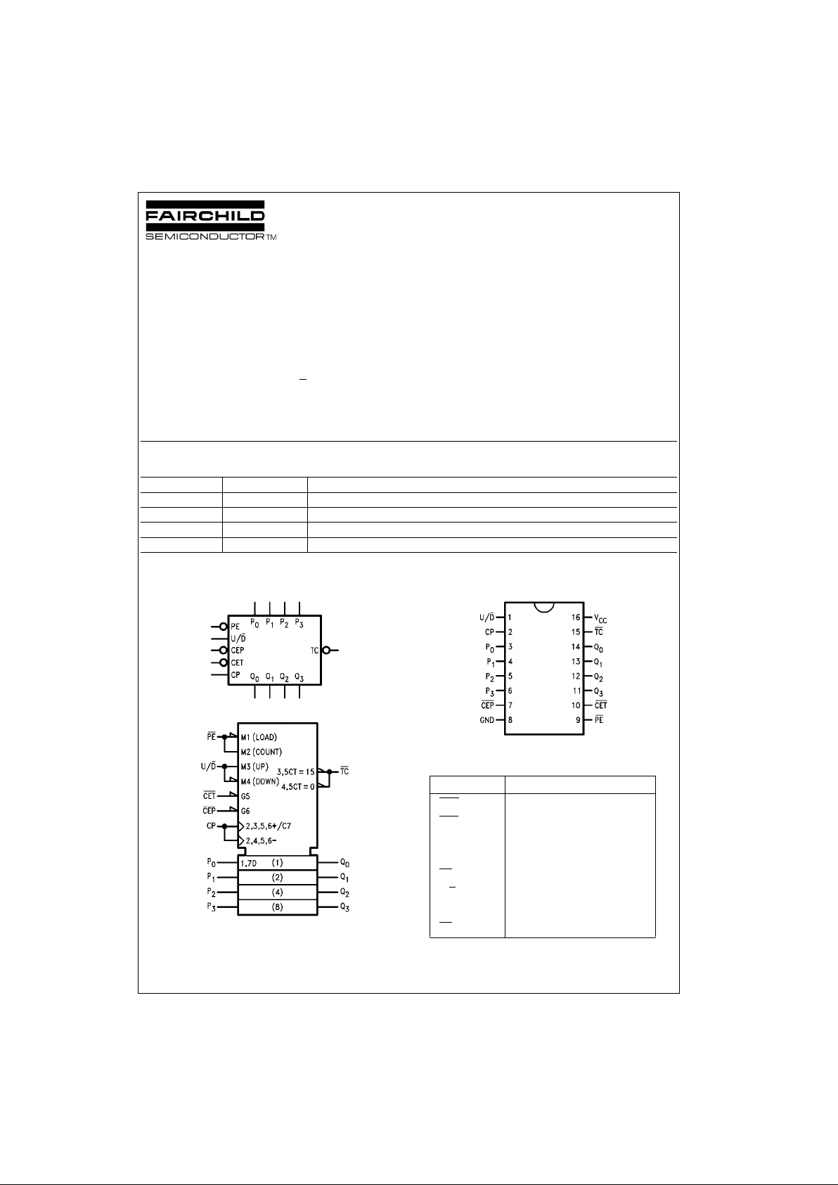
Logic Symbols
IEEE/IEC
Connection Diagram
Pin Descriptions
FACT is a trademark of Fairchild Semiconductor Corporation.
Order Number Package Number Package Description
74AC169SC M16A 16-Lead Small Outline Integrated Circuit (SOIC), JEDEC MS-012, 0.150” Narrow Body
74AC169SJ M16D 16-Lead Small Outline Package (SOP), EIAJ TYPE II, 5.3mm Wide
74AC169MTC MTC16 16-Lead Thin Shrink Small Outline Package (TSSOP), JEDEC MO-153, 4.4mm Wide
74AC169PC N16E 16-Lead Plastic Dual-In-Line Package (PDIP), JEDEC MS-001, 0.300” Wide
Pin Names Description
CEP
Count Enable Parallel Input
CET
Count Enable Trickle Input
CP Clock Pulse Input
P
0–P3
Parallel Data Inputs
PE
Parallel Enable Input
U/D
Up-Down Count Control Input
Q
0–Q3
Flip-Flop Outputs
TC
Terminal Count Output
www.fairchildsemi.com 2
74AC169
Functional Description
The AC169 uses edge-triggered J-K-type flip-flops and
have no constraints on changing the control or data input
signals in either state of the Clock. The only requirement is
that the various inpu ts attain the desired state at least a
setup time before the rising edge of the clock and r emain
valid for the recomm ended h old time the reafter. The para llel load operation ta kes precedence over the other operations, as indicated i n the Mode Select Table. When PE
is
LOW, the data on the P
0–P3
inputs enters the flip-f lops on
the next rising e dge of the Clock. In order for counting to
occur, both CEP
and CET must be LOW and PE mu st be
HIGH; the U/D
input then determines the direction of count-
ing. The Terminal Count (TC
) output is norm ally HIG H an d
goes LOW, provided that CET
is LOW, when a counter
reaches zero in th e C o un t Do wn mo d e or re ac h es 15 i n the
Count Up mode. Th e TC
output state is not a function of
the Count Enable Parallel (CEP
) input level. If an illegal
state occurs, the AC169 will return to the legitimate
sequence within two counts. S ince the TC
signal is derived
by decoding the flip-flop states, there exists the po ssibility
of decoding spikes on TC
. For this reason the use of TC as
a clock signal is no t recommended (see logic equations
below).
1. Count Enable = CEP
•CET • PE
2. Up: TC = Q0•Q1•Q 2Q3•(Up)•CET
3. Down: TC = Q0• Q1•Q2•Q3 •(Down)•CET
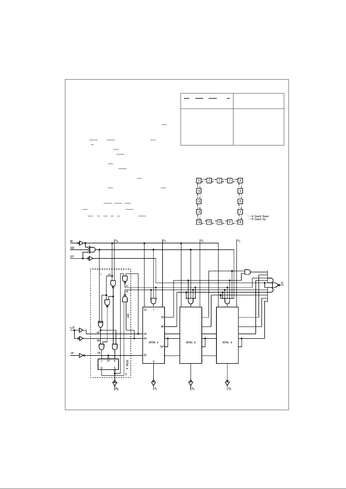
Mode Select Table
H = HIGH Voltage Level
L = LOW Voltage Level
X = Immaterial
State Diagram
Logic Diagram
Please note that this diagram is provided only for the understanding of logic operations and should not be used to estimate propagation delays.
PE CEP CET U/D
Action on Rising
Clock Edge
L X X X Load (P
n
to Qn)
H L L H Count Up (Increment)
H L L L Count Down (Decrement)
H H X X No Change (Hold)
H X H X No Change (Hold)
3 www.fairchildsemi.com
74AC169
Absolute Maximum Ratings(Note 1) Recommended Operating
Conditions
Note 1: Absolute max imum ratings are those values beyond w hich damage
to the device may occu r. The databook spe cificatio ns shou ld be met, wit hout exception, to ensure that the system de sign is relia ble over its p ower
supply, temperature, and output/input loading variables. Fairchild does not
recommend operation of FACT circuits outside databook specif ic at ions.
DC Electrical Characteristics
Note 2: All outputs loaded; thres holds on input associate d w it h output under test.
Note 3: Maximum test duration 2.0 ms, one output loaded at a time.
Note 4: I
IN
and ICC @ 3.0V are guaranteed to be less than or equa l t o th e respective limit @ 5.5V VCC.
Supply Voltage (VCC) −0.5V to +7.0V
DC Input Diode Current (I
IK
)
V
I
= −0.5V −20 mA
V
I
= VCC + 0.5V +20 mA
DC Input Voltage (V
I
) −0.5V to VCC + 0.5V
DC Output Diode Current (I
OK
)
V
O
= −0.5V −20 mA
V
O
= VCC + 0.5V +20 mA
DC Output Voltage (V
O
) −0.5V to VCC + 0.5V
DC Output S ource
or Sink Current (I
O
) ±50 mA
DC V
CC
or Ground Current
per Output Pin (I
CC
or I
GND
) ±50 mA
Storage Temperature (T
STG
) −65°C to +150°C
Junction Temperature (T
J
)
PDIP 140°C
Supply Voltage (V
CC
) 2.0V to 6.0V
Input Voltage (V
I
)0V to V
CC
Output Voltage (VO)0V to V
CC
Operating Temperature (TA) −40°C to +85°C
Minimum Input Edge Rate (∆V/∆t)
V
IN
from 30% to 70% of V
CC
VCC @ 3.3V, 4.5V, 5.5V 125 mV/ns
Symbol Parameter
V
CC
(V)
TA = +25°C TA = −40°C to +85°C
Units Conditions
Typ Guaranteed Limits
V
IH
Minimum HIGH Level 3.0 1.5 2.1 2.1 V
OUT
= 0.1V
Input Voltage 4.5 2.25 3.15 3.15 V or VCC − 0.1V
5.5 2.75 3.85 3.85
V
IL
Maximum LOW Level 3.0 1.5 0.9 0.9 V
OUT
= 0.1V
Input Voltage 4.5 2.25 1.35 1.35 V or VCC − 0.1V
5.5 2.75 1.65 1.65
V
OH
Minimum HIGH Level 3.0 2.99 2.9 2.9
Output Voltage 4.5 4.49 4.4 4.4 V I
OUT
= −50 µA
5.5 5.49 5.4 5.4
VIN = V
IL
or V
IH
3.0 2.56 2.46 IOH = −12 mA
4.5 3.86 3.76 V I
OH
= −24 mA
5.5 4.86 4.76 IOH = −24 mA (Note 2)
V
OL
Maximum LOW Level 3.0 0.002 0.1 0.1
Output Voltage 4.5 0.001 0.1 0.1 V I
OUT
= 50 µA
5.5 0.001 0.1 0.1
VIN = V
IL
or V
IH
3.0 0.36 0.44 IOL = 12 mA
4.5 0.36 0.44 V IOL = 24 mA
5.5 0.36 0.44 IOL = 24 mA (Note 2)
I
IN
Maximum Input
5.5 ±0.1 ±1.0 µAVI = VCC, GND
(Note 4) Leakage Current
I
OLD
Minimum Dynamic 5.5 75 mA V
OLD
= 1.65V Max
I
OHD
Output Current (Note 3) 5.5 −75 mA V
OHD
= 3.85V Min
I
CC
Maximum Quiescent
5.5 4.0 40.0 µA
VIN = V
CC
(Note 4) Supply Current or GND
 Loading...