


100360QIX
Fairchild Semiconductor 100360QIX, 100360QI, 100360QCX, 100360QC, 100360PC Datasheet
...
© 2000 Fairchild Semiconductor Corporation DS010611 www.fairchildsemi.com
March 1998
Revised August 2000
100360 Low Power Dual Parity Checker/Generator
100360
Low Power Dual Parity Checker/Generator
General Description
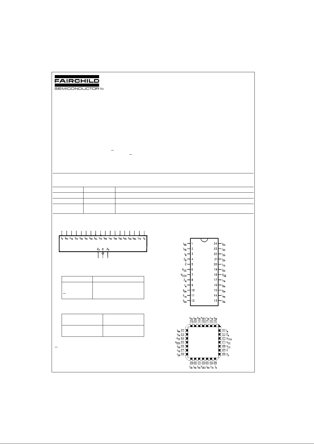
The 100360 is a du al parity checker/gener ator. Each half
has nine inputs; the o utput is HIGH whe n an e ven nu mber
of inputs are HIGH. One of the nine inputs (I
a
or Ib) has the
shorter through-p ut dela y and is th erefo re pr eferre d as t he
expansion input for gene rating parity for 16 or more bits.
The 100360 also has a Comp are (C
) output which allows
the circuit to compare two 8-bit words. The C
output is
LOW when the two wor ds mat ch, bi t f or bit. A ll in pu ts ha ve
50 k
Ω pull-down resistors.
Features
■ Lower power than 100160
■ 2000V ESD protection
■ Pin/function compatible with 100160
■ Voltage compensated operating range
= −4.2V to −5.7V
■ Min to Max propagation delay 35% tight er tha n 1001 60
■ Available to industrial grade temperature range
Ordering Code:
Devices also availab le in Tape and Reel. Specify by appending th e s uffix let t er “X” to the ordering code.
Logic Symbol
Pin Descriptions
Truth Table
(Each Half)
Comparator Function
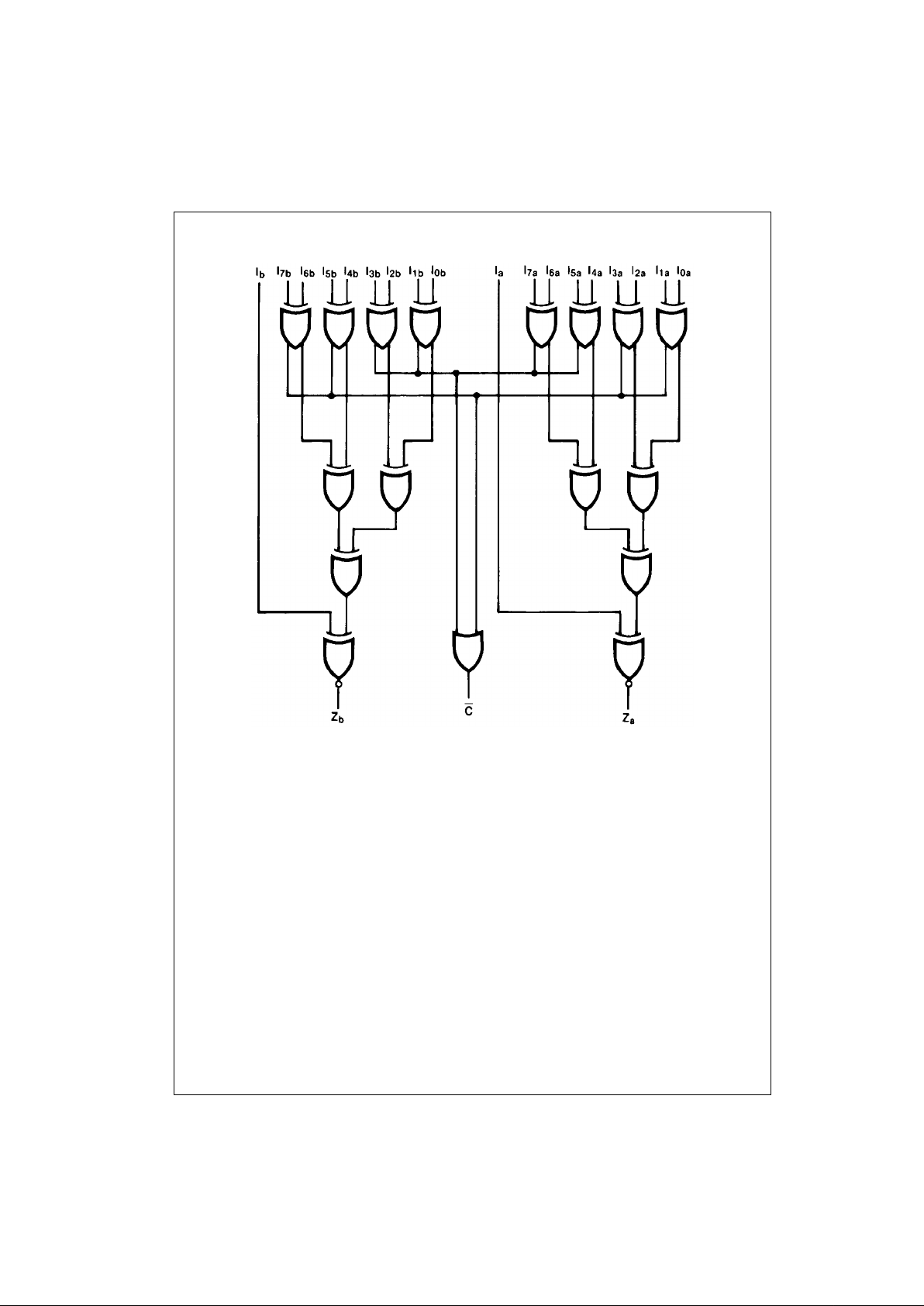
C = (I0a ⊕ I1a) + (I2a ⊕ I3a) + (I4a ⊕ I5a) + (I6a ⊕ I7a) +
(I
0b
⊕ I1b) + (I2b ⊕ I3b) + (I4b ⊕ I5b) + (I6b ⊕ I7b)
Connection Diagrams
24-Pin DIP
28-Pin PLCC
Order Number Package Number Package Description
100360PC N24E 24-Lead Plastic Dual-In-Line Package (PDIP), JEDEC MS-010, 0.400 Wide
100360QC V28A 28-Lead Plastic Lead Chip Carrier (PLCC), JEDEC MO-047, 0.450 Square
100360QI V28A 28-Lead Plastic Lead Chip Carrier (PLCC), JEDEC MO-047, 0.450 Square
Industrial Temperature Range (
−40°C to +85°C)
Pin Names Description
I
a
, Ib, Ina, I
nb
Data Inputs
Z
a
, Z
b
Parity Odd Outputs
C
Compare Output
Sum of Output
HIGH Inputs Z
Even HIGH
Odd LOW
www.fairchildsemi.com 2
100360
Logic Diagram

3 www.fairchildsemi.com
100360
Absolute Maximum Ratings(Note 1) Recommended Operating
Conditions
Note 1: The “Absolute Maximum Ratings” are those value s beyond which
the safety of the dev ice cannot b e guaranteed . The device sh ould not be
operated at these limit s. The parametric values defi ned in the Electrical
Characteristics tables are not guaranteed at the absolute maximum rating.
The “Recomm ended O peratin g Cond itions ” table will defin e the condition s
for actual device operation.
Note 2: ESD testing conforms to MIL-STD-883, Method 3015.
Commercial Version
DC Electrical Characteristics
(Note 3)
V
EE
= −4.2V to −5.7V, VCC = V
CCA
= GND, T
C
= 0°C to +85°C
Note 3: The specified limits represent the ''wors t case” value for the parameter. Since these values normally occur at the temperature extremes, additional
noise immunity and guardbanding can be achieved by decreasin g the al l owable syste m opera ti ng ran ge s. Cond it i ons fo r t estin g sho w n in the tabl es are chosen to guarantee operation under “worst case” conditions.
DIP AC Electrical Characteristics
V
EE
= −4.2V to −5.7V, VCC = V
CCA
= GND
Storage Temperature (T
STG
) −65°C to +150°C
Maximum Junction Temperature (T
J
) +150°C
V
EE
Pin Potential to Ground Pin −7.0V to +0.5V
Input Voltage (DC) V
EE
to +0.5V
Output Current (DC Output HIGH)
−50 mA
ESD (Note 2)
≥2000V
Case Temperature (T
C
)
Commercial 0
°C to +85°C
Industrial
−40°C to +85°C
Supply Voltage (V
EE
) −5.7V to −4.2V
Symbol Parameter Min Typ Max Units Conditions
V
OH
Output HIGH Voltage −1025 −955 −870
mV
VIN = VIH (Max) Loading with
V
OL
Output LOW Voltage −1830 −1705 −1620 or V
IL (Min)
50Ω to −2.0V
V
OHC
Output HIGH Voltage −1035
mV
VIN = VIH (Min) Loading with
V
OLC
Output LOW Voltage −1610 or V
IL (Max)
50Ω to −2.0V
V
IH
Input HIGH Voltage −1165 −870 mV Guaranteed HIGH Signal
for All Inputs
V
IL
Input LOW Voltage −1830 −1475 mV Guaranteed LOW Signal
for All Inputs
I
IL
Input LOW Current 0.50 µAVIN = VIL (Min)
I
IH
Input HIGH Current
I
a
, I
b
340 µAVIN = VIH (Max)
I
na
, I
nb
240
I
EE
Power Supply Current −100 −50 mA Inputs OPEN
Symbol Parameter
T
C
= 0°CT
C
= +25°CT
C
= +85°C
Units Conditions
Min Max Min Max Min Max
t
PLH
Propagation Delay
1.10 2.75 1.10 2.75 1.10 2.75 ns
t
PHL
Ina, Inb to Za, Z
b
t
PLH
Propagation Delay
1.10 2.80 1.10 2.80 1.10 2.80 ns
t
PHL
Ina, Inb to C Figures 1, 2
t
PLH
Propagation Delay
0.50 1.20 0.60 1.30 0.60 1.30 ns
t
PHL
Ia, Ib to Za, Z
b
t
TLH
Transition Time
0.35 1.10 0.35 1.10 0.35 1.10 ns
t
THL
20% to 80%, 80% to 20%
 Loading...