


Texas Instruments THS1031IPWR, THS1031IPW, THS1031IDWR, THS1031IDW, THS1031CPWR Datasheet
...THS1031 2.7 V ± 5.5 V, 10-BIT, 30 MSPS CMOS ANALOG-TO-DIGITAL CONVERTER
SLAS242A ± NOVEMBER 1999 ± REVISED JANUARY 2000
D |
10-Bit Resolution 30 MSPS |
28-PIN TSSOP/SOIC PACKAGE |
||||||||
|
Analog-to-Digital Converter: |
|
(TOP VIEW) |
|
|
|
||||
D |
Configurable Input Functions: |
AGND |
|
|
|
|
|
AVDD |
||
|
|
1 |
28 |
|
||||||
|
|
|
||||||||
|
± Single-Ended |
|
|
|||||||
|
DVDD |
|
|
2 |
27 |
|
AIN |
|||
|
± Single-Ended With Analog Clamp |
|
|
|||||||
|
I/O0 |
|
|
3 |
26 |
|
VREF |
|||
|
± Single-Ended With Programmable Digital |
|
|
|||||||
|
I/O1 |
4 |
25 |
|
REFBS |
|||||
|
Clamp |
|
||||||||
|
I/O2 |
|
|
|
|
|
REFBF |
|||
|
5 |
24 |
|
|||||||
|
± Differential |
|
||||||||
|
I/O3 |
|
|
6 |
23 |
|
MODE |
|||
D Built-in Programmable Gain Amplifier |
|
|
||||||||
I/O4 |
7 |
22 |
|
REFTF |
||||||
|
(PGA) |
|
||||||||
|
I/O5 |
|
|
|
|
|
REFTS |
|||
|
8 |
21 |
|
|||||||
|
Differential Nonlinearity: ±0.3 LSB |
|
||||||||
D |
I/O6 |
|
9 |
20 |
|
CLAMPIN |
||||
|
|
|||||||||
D |
Signal-to-Noise: 56 dB |
I/O7 |
|
10 |
19 |
|
CLAMP |
|||
D |
Spurious Free Dynamic Range: 60 dB |
I/O8 |
|
11 |
18 |
|
REFSENSE |
|||
D Adjustable Internal Voltage Reference |
I/O9 |
|
12 |
17 |
|
WR |
||||
OVR |
|
|
|
|
|
|
|
|
||
D Straight Binary/2s Complement Output |
13 |
16 |
|
OE |
||||||
DGND |
|
|
|
|
|
CLK |
||||
|
14 |
15 |
|
|||||||
|
|
|
||||||||
DOut-of-Range Indicator
DPower-Down Mode
description
The THS1031 is a CMOS, low power, 10-bit, 30 MSPS analog-to-digital converter (ADC) that can operate with a supply range from 2.7 V to 3.3 V. The THS1031 has been designed to give circuit developers more flexibility. The analog input to the THS1031 can be either single-ended or differential. This device has a built-in clamp amplifier whose clamp input level can be selected from an external dc source or from an internal high-precision 10-bit digital clamp level programmable via an internal CLAMP register. A 3-bit PGA is included to maintain SNR for small signal. The THS1031 provides a wide selection of voltage reference to match the user's design requirements. For more design flexibility, the internal reference can be bypassed to use an external reference to suit the dc accuracy and temperature drift requirements of the application. The out-of-range output is used to monitor any out-of-range condition in THS1031's input range. The format of digital output can be coded in either straight binary or 2s complement.
The speed, resolution, and single-supply operation of the THS1031 are suited for applications in set-top-box (STB), video, multimedia, imaging, high-speed acquisition, and communications. The built-in clamp function allows dc restoration of video signal and is suitable for video application. The speed and resolution ideally suit charge-couple device (CCD) input systems such as color scanners, digital copiers, digital cameras, and camcorders. A wide input voltage range between REFBS and REFTS allows the THS1031 to be applied in both imaging and communications systems
The THS1031I is characterized for operation from ±40°C to 85°C.
AVAILABLE OPTIONS
TA |
PACKAGED DEVICES |
||
|
|
||
28-TSSOP (PW) |
28-SOIC (DW) |
||
|
|||
|
|
|
|
0°C to 70°C |
THS1031CPW |
THS1031CDW |
|
|
|
|
|
± 40°C to 85°C |
THS1031IPW |
THS1031IDW |
|
Please be aware that an important notice concerning availability, standard warranty, and use in critical applications of Texas Instruments semiconductor products and disclaimers thereto appears at the end of this data sheet.
PRODUCTION DATA information is current as of publication date. Products conform to specifications per the terms of Texas Instruments standard warranty. Production processing does not necessarily include testing of all parameters.
Copyright 2000, Texas Instruments Incorporated
POST OFFICE BOX 655303 •DALLAS, TEXAS 75265 |
1 |

THS1031
2.7 V ± 5.5 V, 10-BIT, 30 MSPS
CMOS ANALOG-TO-DIGITAL CONVERTER
SLAS242A ± NOVEMBER 1999 ± REVISED JANUARY 2000
functional block diagram
|
|
|
Power |
|
|
|
|
|
CLAMP |
Down |
|
|
|
|
|
|
|
|
||
|
|
DAC |
10 |
|
|
|
CLAMPIN |
|
|
|
WR |
||
|
|
|
|
|||
|
|
|
|
CTL |
|
|
CLAMP |
SW2 |
|
|
REG |
|
|
|
SW1 |
|
|
BIN/2'S |
|
|
|
|
3 |
|
|
||
|
|
|
|
|
||
AIN |
SHA |
PGA |
A/D |
Output |
I/O0 ± |
|
REFTS |
Buffers |
I/O9 |
||||
|
|
|
||||
|
|
|
|
|
||
|
|
DAC |
REF |
|
|
|
REFBS |
|
|
|
|
|
|
MODE |
|
DC |
|
|
OVR |
|
|
|
|
|
|||
|
|
|
|
|
||
|
|
REF |
|
|
OE |
|
|
|
|
|
|
|
SW3 |
Timing |
|
|
|
REFTF |
|
Circuit |
REFBF |
VBG |
|
|
|
|
|
|
SW4 |
REFSENSE |
VREF |
CLK |
2 |
POST OFFICE BOX 655303 •DALLAS, TEXAS 75265 |

|
|
|
|
|
THS1031 |
|
|
|
|
|
|
2.7 V ± 5.5 V, 10-BIT, 30 MSPS |
|
|
|
|
|
|
CMOS ANALOG-TO-DIGITAL CONVERTER |
|
|
|
|
|
|
SLAS242A ± NOVEMBER 1999 ± REVISED JANUARY 2000 |
|
|
|
|
|
|
|
|
|
|
|
|
|
Terminal Functions |
|
|
|
|
|
|
|
|
|
|
TERMINAL |
|
I/O |
DESCRIPTION |
|
|
|
NAME |
NO. |
|
||
|
|
|
|
|
||
|
|
|
|
|
|
|
|
AGND |
1 |
I |
Analog ground |
|
|
|
|
|
|
|
|
|
|
AIN |
27 |
I |
Analog input |
|
|
|
|
|
|
|
|
|
|
AVDD |
28 |
I |
Analog supply |
|
|
|
CLAMP |
19 |
I |
HI to enable CLAMP mode, LO to disable CLAMP mode |
|
|
|
|
|
|
|
|
|
|
CLAMPIN |
20 |
I |
Connect to an external analog clamp reference input. |
|
|
|
|
|
|
|
|
|
|
CLK |
15 |
I |
Clock input |
|
|
|
|
|
|
|
|
|
|
DGND |
14 |
I |
Digital ground |
|
|
|
|
|
|
|
|
|
|
DVDD |
2 |
I |
Digital driver supply |
|
|
|
I/O0 |
3 |
|
Digital I/O bit 0 (LSB) |
|
|
|
I/O1 |
4 |
|
Digital I/O bit 1 |
|
|
|
I/O2 |
5 |
|
Digital I/O bit 2 |
|
|
|
I/O3 |
6 |
|
Digital I/O bit 3 |
|
|
|
I/O4 |
7 |
I/O |
Digital I/O bit 4 |
|
|
|
I/O5 |
8 |
Digital I/O bit 5 |
|
||
|
|
|
||||
|
I/O6 |
9 |
|
Digital I/O bit 6 |
|
|
|
I/O7 |
10 |
|
Digital I/O bit 7 |
|
|
|
I/O8 |
11 |
|
Digital I/O bit 8 |
|
|
|
I/O9 |
12 |
|
Digital I/O bit 9 (MSB) |
|
|
|
|
|
|
|
|
|
|
MODE |
23 |
I |
Mode input |
|
|
|
|
|
|
|
|
|
|
|
|
16 |
I |
HI to the 3-state data bus, LO to enable the data bus |
|
|
OE |
|
|
|||
|
|
|
|
|
|
|
|
OVR |
13 |
O |
Out-of-range indicator |
|
|
|
|
|
|
|
|
|
|
REFBS |
25 |
I |
Reference bottom sense |
|
|
|
|
|
|
|
|
|
|
REFBF |
24 |
I |
Reference bottom decoupling |
|
|
|
|
|
|
|
|
|
|
REFSENSE |
18 |
I |
Reference sense |
|
|
|
|
|
|
|
|
|
|
REFTF |
22 |
I |
Reference top decoupling |
|
|
|
|
|
|
|
|
|
|
REFTS |
21 |
I |
Reference top sense |
|
|
|
|
|
|
|
|
|
|
VREF |
26 |
I/O |
Internal and external reference for ADC |
|
|
|
WR |
17 |
I |
Write strobe goes HI to write data value D0:D9 to the internal registers. |
|
|
|
|
|
|
|
|
|
POST OFFICE BOX 655303 •DALLAS, TEXAS 75265 |
3 |

THS1031
2.7 V ± 5.5 V, 10-BIT, 30 MSPS
CMOS ANALOG-TO-DIGITAL CONVERTER
SLAS242A ± NOVEMBER 1999 ± REVISED JANUARY 2000
absolute maximum ratings over operating free-air temperature (unless otherwise noted)²
Supply voltage: AVDD to AGND, DVDD to DGND . . . . . . . . . . . . . . . . . . . . . . . . . . . . . . . |
. . . . . . . ±0.3 to 6.5 V |
|
AGND to DGND . . . . . . . . . . . . . . . . . . . . . . . . . . . . . . . . . . . . . . . . . . . . . . . |
. . . . . . ±0.3 to 0.3 V |
|
AVDD to DVDD . . . . . . . . . . . . . . . . . . . . . . . . . . . . . . . . . . . . . . . . . . . . . . . . |
. . . . . . ±6.5 to 6.5 V |
|
Mode input MODE to AGND . . . . . . . . . . . . . . . . . . . . . . . . . . . . . . . . . . . . . . . . . . . . . . . . . . |
±0.3 to AVDD + 0.3 V |
|
Reference voltage input range REFTF, REFTB, REFTS, REFBS to AGND . . . . . . . . . |
±0.3 to AVDD + 0.3 V |
|
Analog input voltage range AIN to AGND . . . . . . . . . . . . . . . . . . . . . . . . . . . . . . . . . . . . . . |
±0.3 to AVDD + 0.3 V |
|
Reference input VREF to AGND . . . . . . . . . . . . . . . . . . . . . . . . . . . . . . . . . . . . . . . . . . . . . . |
±0.3 to AVDD + 0.3 V |
|
Reference output VREF to AGND . . . . . . . . . . . . . . . . . . . . . . . . . . . . . . . . . . . . . . . . . . . . . |
±0.3 to AVDD + 0.3 |
V |
Clock input CLK to AGND . . . . . . . . . . . . . . . . . . . . . . . . . . . . . . . . . . . . . . . . . . . . . . . . . . . . |
±0.3 to AVDD + 0.3 |
V |
Digital input to DGND . . . . . . . . . . . . . . . . . . . . . . . . . . . . . . . . . . . . . . . . . . . . . . . . . . . . . . . . |
±0.3 to DVDD + 0.3 |
V |
Digital output to DGND . . . . . . . . . . . . . . . . . . . . . . . . . . . . . . . . . . . . . . . . . . . . . . . . . . . . . . |
±0.3 to DVDD + 0.3 |
V |
Operating junction temperature range, TJ . . . . . . . . . . . . . . . . . . . . . . . . . . . . . . . . . . . . . . . |
. . . . . . 0°C to 150°C |
|
Storage temperature range, TSTG . . . . . . . . . . . . . . . . . . . . . . . . . . . . . . . . . . . . . . . . . . . . . . |
. . . ±65°C to 150°C |
|
Lead temperature 1,6 mm (1/16 in) from case for 10 seconds . . . . . . . . . . . . . . . . . . . . . . |
. . . . . . . . . . . . 300°C |
|
²Stresses beyond those listed under ªabsolute maximum ratingsº may cause permanent damage to the device. These are stress ratings only, and functional operation of the device at these or any other conditions beyond those indicated under ªrecommended operating conditionsº is not implied. Exposure to absolute-maximum-rated conditions for extended periods may affect device reliability.
recommended operating conditions digital inputs
|
|
|
|
|
MIN NOM |
MAX |
UNIT |
|
|||
|
|
|
|
|
|
|
|
|
|
|
|
High-level input voltage, VIH |
2.4 |
|
|
V |
|
||||||
Low-level input voltage, VIL |
|
|
|
|
0.2 x DVDD |
V |
|
||||
analog inputs |
|
|
|
|
|
|
|
|
|
|
|
|
|
|
|
|
|
|
|
|
|
|
|
|
|
|
|
|
|
|
MIN |
NOM |
MAX |
UNIT |
|
|
|
|
|
|
|
|
|
|
|
|
|
Analog input voltage, VI(AIN) |
|
REFBS |
|
REFTS |
V |
|
|||||
Reference input voltage, VI(VREF) |
|
1 |
|
2 |
V |
|
|||||
Reference input voltage, VI(REFTS) |
|
1 |
|
AVDD |
V |
|
|||||
Reference input voltage, VI(REFBS) |
|
0 |
AVDD±1 |
V |
|
||||||
Clamp input voltage, VI(CLAMPIN) |
|
REFBS |
|
REFTS |
V |
|
|||||
power supply |
|
|
|
|
|
|
|
|
|
|
|
|
|
|
|
|
|
|
|
|
|
|
|
|
|
|
|
|
|
|
MIN |
NOM |
MAX |
UNIT |
|
|
|
|
|
|
|
|
|
|
|
|
|
Supply voltage |
Maximum sampling rate = 30 MSPS |
AVDD |
|
|
|
2.7 |
3 |
5.5 |
V |
|
|
DVDD |
|
|
|
2.7 |
3 |
5.5 |
|
||||
|
|
|
|
|
|
|
|||||
REFTS, REFBS reference voltages (MODE = AVDD) |
|
|
|
|
|
|
|
|
|||
|
|
PARAMETER |
|
|
|
MIN |
TYP |
MAX |
UNIT |
|
|
|
|
|
|
|
|
|
|
||||
REFTS |
Reference input voltage (top) |
|
|
1 |
|
AVDD |
V |
|
|||
REFBS |
Reference input voltage (bottom) |
|
|
0 |
AVDD±1 |
V |
|
||||
|
Differential input (REFTS ± REFBS) |
|
|
1 |
|
2 |
V |
|
|||
|
|
|
|
|
|
|
|
|
|
||
|
Switched input capacitance on REFTS |
|
|
|
|
0.6 |
|
pF |
|
||
|
|
|
|
|
|
|
|
|
|
||
|
Switched input capacitance on REFBS |
|
|
|
|
0.6 |
|
pF |
|
||
sampling rate and resolution |
|
|
|
|
|
|
|
|
|||
|
|
|
|
|
|
|
|
|
|
|
|
|
|
PARAMETER |
|
|
|
MIN |
NOM |
MAX |
UNIT |
|
|
|
|
|
|
|
|
|
|
|
|
||
Fs |
|
|
|
|
|
|
5 |
|
30 |
MHz |
|
|
|
|
|
|
|
|
|
|
|
|
|
Resolution |
|
|
|
|
|
|
|
10 |
|
Bits |
|
|
|
|
|
|
|
|
|
|
|
|
|
|
|
|
|
|
|
|
|
|
|
|
|
4 |
POST OFFICE BOX 655303 •DALLAS, TEXAS 75265 |

THS1031 2.7 V ± 5.5 V, 10-BIT, 30 MSPS CMOS ANALOG-TO-DIGITAL CONVERTER
SLAS242A ± NOVEMBER 1999 ± REVISED JANUARY 2000
electrical characteristics, AVDD = 3 V, DVDD = 3 V, Fs = 30 MSPS/50% duty cycle, MODE = AVDD, 2 V input span from 0.5 V to 2.5 V, external reference, PGA = 1X, TA = ±40°C to 85°C (unless otherwise noted)
analog inputs
|
PARAMETER |
MIN |
TYP |
MAX |
UNIT |
|
|
|
|
|
|
VI(AIN) |
Analog input voltage |
REFBS |
|
REFTS |
V |
CI |
Switched input capacitance |
|
1.2 |
|
pF |
FPBW |
Full power BW (±3 dB) |
|
150 |
|
MHz |
|
|
|
|
|
|
|
DC leakage current (input = ± FS) |
|
100 |
|
µA |
REFTF, REFBF reference voltages
|
PARAMETER |
TEST CONDITIONS |
MIN |
TYP |
MAX |
UNIT |
|
|
|
|
|
|
|
|
|
Differential input (REFTF ± REFBF) |
|
1 |
|
2 |
V |
||
|
|
|
|
|
|
|
|
Input common mode (REFTF + REFBF)/2 |
AVDD = 3 V |
1.3 |
1.5 |
1.7 |
V |
||
AVDD = 5 V |
2 |
2.5 |
3 |
||||
|
|
|
|||||
|
VREF = 1 V |
AVDD = 3 V |
|
2 |
|
V |
|
REFTF (MODE = AVDD) |
AVDD = 5 V |
|
3 |
|
|||
|
|
|
|
||||
VREF = 2 V |
AVDD = 3 V |
|
2.5 |
|
V |
||
|
|
|
|||||
|
AVDD = 5 V |
|
3.5 |
|
|||
|
|
|
|
|
|||
|
VREF = 1 V |
AVDD = 3 V |
|
1 |
|
V |
|
REFBF (MODE = AVDD) |
AVDD = 5 V |
|
0.5 |
|
|||
|
|
|
|
||||
VREF = 2 V |
AVDD = 3 V |
|
2 |
|
V |
||
|
|
|
|||||
|
AVDD = 5 V |
|
1.5 |
|
|||
|
|
|
|
|
|||
Input resistance between REFTF and REFBF |
|
|
600 |
|
Ω |
||
VREF reference voltages
|
PARAMETER |
MIN |
TYP |
MAX |
UNIT |
|
|
|
|
|
|
|
Internal 1 V reference (REFSENSE = VREF) |
0.95 |
1 |
1.05 |
V |
|
Internal 2 V reference (REFSENSE = AVSS) |
1.90 |
2 |
2.10 |
V |
|
External reference (REFSENSE = AVDD) |
1 |
|
2 |
V |
|
Reference input resistance |
|
18 |
|
kΩ |
dc accuracy |
|
|
|
|
|
|
|
|
|
|
|
|
PARAMETER |
MIN |
TYP |
MAX |
UNIT |
|
|
|
|
|
|
INL |
Integral nonlinearity |
|
± 1 |
± 2 |
LSB |
|
|
|
|
|
|
DNL |
Differential nonlinearity |
|
± 0.3 |
± 1 |
LSB |
|
|
|
|
|
|
|
Offset error |
|
0.4 |
1.4 |
%FSR |
|
|
|
|
|
|
|
Gain error |
|
1.4 |
3.5 |
%FSR |
|
|
|
|
||
|
Missing code |
No missing code assured |
|||
POST OFFICE BOX 655303 •DALLAS, TEXAS 75265 |
5 |

THS1031
2.7 V ± 5.5 V, 10-BIT, 30 MSPS
CMOS ANALOG-TO-DIGITAL CONVERTER
SLAS242A ± NOVEMBER 1999 ± REVISED JANUARY 2000
electrical characteristics, AVDD = 3 V, DVDD = 3 V, Fs = 30 MSPS/50% duty cycle, MODE = AVDD, 2 V input span from 0.5 V to 2.5 V, external reference, PGA = 1X, TA = ±40°C to 85°C (unless otherwise noted) (continued)
dynamic performance (ADC and PGA)
|
PARAMETER |
TEST CONDITIONS |
MIN |
TYP |
MAX |
UNIT |
|
|
|
|
|
|
|
|
|
f = 3.5 MHz |
8.2 |
9 |
|
|
|
|
|
|
|
|
|
ENOB |
Effective number of bits |
f = 3.5 MHz, AVDD = 5 V |
|
8.8 |
|
Bits |
f = 15 MHz |
|
7.7 |
|
|||
|
|
|
|
|
||
|
|
|
|
|
|
|
|
|
f = 15 MHz, AVDD = 5 V |
|
7.64 |
|
|
|
|
f = 3.5 MHz |
55 |
60 |
|
|
|
|
|
|
|
|
|
SFDR Spurious free dynamic range |
f = 3.5 MHz, AVDD = 5 V |
|
63 |
|
dB |
|
f = 15 MHz |
|
48 |
|
|||
|
|
|
|
|
||
|
|
|
|
|
|
|
|
|
f = 15 MHz, AVDD = 5 V |
|
52.4 |
|
|
|
|
f = 3.5 MHz |
|
± 58.2 |
± 54.7 |
|
|
|
|
|
|
|
|
THD |
Total harmonic distortion |
f = 3.5 MHz, AVDD = 5 V |
|
± 68.7 |
|
dB |
f = 15 MHz |
|
± 47 |
|
|||
|
|
|
|
|
||
|
|
|
|
|
|
|
|
|
f = 15 MHz, AVDD = 5 V |
|
± 51.9 |
|
|
|
|
f = 3.5 MHz |
51.2 |
56 |
|
|
|
|
|
|
|
|
|
SNR |
Signal-to-noise |
f = 3.5 MHz, AVDD = 5 V |
|
55 |
|
dB |
f = 15 MHz |
|
53 |
|
|||
|
|
|
|
|
||
|
|
|
|
|
|
|
|
|
f = 15 MHz, AVDD = 5 V |
|
49.3 |
|
|
|
|
f = 3.5 MHz |
51.1 |
56 |
|
|
|
|
|
|
|
|
|
SINAD |
Signal-to-noise and distortion |
f = 3.5 MHz, AVDD = 5 V |
|
55 |
|
dB |
f = 15 MHz |
|
48.1 |
|
|||
|
|
|
|
|
||
|
|
|
|
|
|
|
|
|
f = 15 MHz, AVDD = 5 V |
|
47.7 |
|
|
PGA |
|
|
|
|
|
|
PARAMETER |
MIN |
TYP |
MAX |
UNIT |
|
|
|
|
|
Gain range (linear scale) |
0.5 |
|
4 |
V/V |
|
|
|
|
|
Gain step size (linear scale) |
|
0.5 |
|
|
|
|
|
|
|
Gain error from nominal |
|
|
3% |
|
|
|
|
|
|
Number of control bits |
|
3 |
|
Bits |
clamp DAC
PARAMETER |
MIN |
TYP |
MAX |
UNIT |
|
|
|
|
|
Resolution |
|
10 |
|
Bits |
|
|
|
|
|
DAC output range |
REFBF |
|
REFTF |
|
|
|
|
|
|
Clamping analog output voltage range |
0.1 |
|
AVDD± 0.1 |
V |
Clamping analog output voltage error |
± 40 |
|
+ 40 |
mV |
6 |
POST OFFICE BOX 655303 •DALLAS, TEXAS 75265 |

THS1031 2.7 V ± 5.5 V, 10-BIT, 30 MSPS CMOS ANALOG-TO-DIGITAL CONVERTER
SLAS242A ± NOVEMBER 1999 ± REVISED JANUARY 2000
electrical characteristics, AVDD = 3 V, DVDD = 3 V, Fs = 30 MSPS/50% duty cycle, MODE = AVDD, 2 V input span from 0.5 V to 2.5 V, external reference, PGA = 1X, TA = ±40°C to 85°C (unless otherwise noted) (continued)
clock
|
PARAMETER |
MIN |
TYP MAX |
UNIT |
|
|
|
|
|
tCK |
Clock period |
33 |
|
ns |
tCKH |
Pulse duration, clock high |
15 |
16.5 |
ns |
tCKL |
Pulse duration, clock high |
15 |
16.5 |
ns |
td |
Clock to data valid |
|
25 |
ns |
|
Pipeline latency |
|
3 |
Cycles |
|
|
|
|
|
t(ap) |
Aperture delay |
|
4 |
ns |
|
Aperture uncertainty (jitter) |
|
2 |
ps |
timing
|
PARAMETER |
MIN |
TYP MAX |
UNIT |
|
|
|
|
|
t(PZ) |
Output disable to high-Z output |
0 |
20 |
ns |
t(DEN) |
Output enable to output valid |
0 |
20 |
ns |
t(OEW) |
Output disable to write enable |
12 |
|
ns |
t(WOE) |
Output disable to write enable |
12 |
|
ns |
t(WP) |
Write pulse |
15 |
|
ns |
t(DS) |
Input data setup time |
5 |
|
ns |
t(DH) |
Input data hold time |
5 |
|
ns |
power supply
|
PARAMETER |
TEST CONDITIONS |
MIN TYP |
MAX |
UNIT |
|
|
|
|
|
|
ICC |
Operating supply current |
AVDD = 3 V, MODE = AGND |
30.6 |
45 |
mA |
PD |
Power dissipation |
AVDD = DVDD = 3 V |
94 |
135 |
mW |
AVDD = DVDD = 5 V |
160 |
|
|||
|
|
|
|
||
PD(STBY) |
Standby power |
AVDD = DVDD = 3 V, MODE = AGND |
3 |
5 |
mW |
POST OFFICE BOX 655303 •DALLAS, TEXAS 75265 |
7 |
THS1031
2.7 V ± 5.5 V, 10-BIT, 30 MSPS
CMOS ANALOG-TO-DIGITAL CONVERTER
SLAS242A ± NOVEMBER 1999 ± REVISED JANUARY 2000
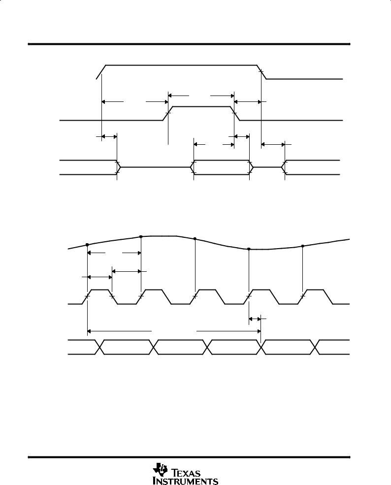
PARAMETER MEASUREMENT INFORMATION
OE |
|
|
|
(See Note A) |
||
|
|
|
|
|
|
|
t(WP)
t(OEW) |
t(WOE) |
WE
|
t(DZ) |
t(DH) |
|
|
|
t(DS) |
t(DEN) |
I/O |
hi±Z |
Input |
hi±Z |
Output |
Output |
NOTE A: All timing measurements are based on 50% of edge transition.
|
|
Figure 1. Write Timing Diagram |
|
|
|
|
|
Sample 2 |
Sample 3 |
|
|
|
|
|
|
|
|
|
Sample 1 |
|
Sample 4 |
Sample 5 |
|
Analog Input |
|
|
|
|
|
|
|
|
|
|
|
|
t(CK) |
|
|
|
|
t(CKH) |
t(CKL) |
|
|
|
|
|
|
|
|
||
Input Clock |
(See |
|
|
|
|
|
Note A) |
|
|
|
|
|
|
|
|
td |
|
|
|
Pipeline Latency |
|
|
|
Digital Output |
|
|
|
Sample 1 |
Sample 2 |
NOTE A: All timing measurements are based on 50% of edge transition.
Figure 2. Digital Output Timing Diagram
8 |
POST OFFICE BOX 655303 •DALLAS, TEXAS 75265 |
 Loading...