


Texas Instruments SN74ALS641A-1DW, SN74ALS641A-1DWR, SN74ALS641A-1N, SN74ALS641ADW, SN74ALS641ADWR Datasheet
...
SN74ALS641A, SN74ALS642A, SN74AS641
OCTAL BUS TRANSCEIVERS
WITH OPEN-COLLECTOR OUTPUTS
SDAS300 ± MARCH 1995
• Bidirectional Bus Transceivers in |
DW OR N PACKAGE |
||||||||
High-Density 20-Pin Packages |
|
(TOP VIEW) |
|
|
|
||||
• Choice of True or Inverting Logic |
DIR |
|
|
|
VCC |
||||
|
1 |
20 |
|||||||
• Package Options Include Plastic |
|
||||||||
|
|
|
|||||||
|
|
|
|
|
|
|
|||
A1 |
|
2 |
19 |
OE |
|||||
Small-Outline (DW) Packages and |
|
||||||||
A2 |
|
3 |
18 |
B1 |
|||||
|
|||||||||
Standard Plastic (N) 300-mil DIPs |
|
||||||||
A3 |
|
4 |
17 |
B2 |
|||||
|
|||||||||
|
|
|
|
||||||
|
|
|
A4 |
|
5 |
16 |
B3 |
||
|
|
|
|
||||||
|
DEVICE |
LOGIC |
A5 |
|
6 |
15 |
B4 |
||
|
|
|
|
||||||
|
SN74ALS641A, SN74AS641 |
True |
A6 |
|
7 |
14 |
B5 |
||
|
|
||||||||
|
SN74ALS642A |
Inverting |
A7 |
|
8 |
13 |
B6 |
||
|
|
||||||||
description |
|
A8 |
|
9 |
12 |
B7 |
|||
|
GND |
|
10 |
11 |
B8 |
||||
|
|
||||||||
|
|
|
|
|
|
|
|
|
|
These octal bus transceivers are designed for asynchronous two-way communication between
data buses. These devices transmit data from the A bus to the B bus or from the B bus to the A bus, depending upon the level at the direction-control (DIR) input. The output-enable (OE) input disables the device so that the buses are effectively isolated.
The -1 versions of the SN74ALS641A and SN74ALS642A are identical to the standard versions, except that the recommended maximum IOL is increased to 48 mA in the -1 versions.
The SN74ALS641A, SN74ALS642A, and SN74AS641 are characterized for operation from 0°C to 70°C.
FUNCTION TABLE
|
INPUTS |
OPERATION |
||||||
|
|
|
|
|
|
|
|
|
|
|
|
SN74ALS641A |
|
|
|
|
|
|
OE |
DIR |
SN74ALS642A |
|||||
|
SN74AS641 |
|||||||
|
|
|
|
|
|
|
|
|
|
|
|
|
|
|
|
|
|
|
L |
L |
B data to A bus |
|
|
data to A bus |
||
|
|
|
B |
|
||||
|
L |
H |
A data to B bus |
|
|
|||
|
|
A |
data to B bus |
|||||
|
H |
X |
Isolation |
|
|
|
|
Isolation |
|
|
|
|
|
|
|
|
|
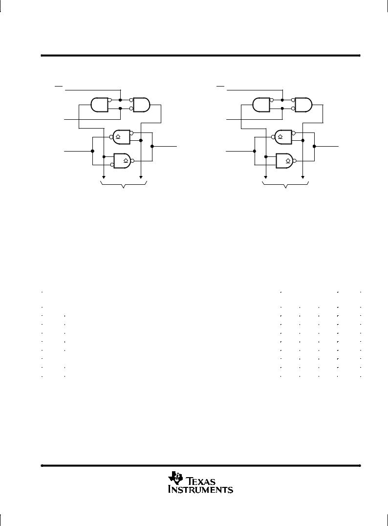
logic symbols²
|
|
|
|
|
|
SN74ALS641A, SN74AS641 |
|
|
|
|
|
|
|
|
SN74ALS642A |
|||||
|
|
|
19 |
|
|
|
|
|
|
|
|
|
|
19 |
|
|
|
|
|
|
|
|
|
|
|
|
G3 |
|
|
|
|
|
|
|
|
|
|
||||
OE |
|
|
|
|
|
OE |
G3 |
|||||||||||||
|
|
|
|
|
|
|
|
|
|
|||||||||||
1 |
|
|
|
|
|
1 |
|
|
|
|||||||||||
DIR |
|
|
|
3 EN1 [BA] |
|
DIR |
|
|
|
3 EN1 [BA] |
||||||||||
|
|
|
|
|
|
|
|
|
||||||||||||
|
|
|
|
|
|
|
3 EN2 [AB] |
|
|
|
|
|
|
|
|
3 EN2 [AB] |
||||
|
|
|
|
|
|
|
|
|
|
|
|
|
|
|
|
|
|
|
|
|
A1 |
2 |
18 |
A1 |
2 |
18 |
1 |
B1 |
1 |
B1 |
||
|
2 |
|
|
|
2 |
A2 |
3 |
17 |
A2 |
3 |
17 |
|
B2 |
|
B2 |
||
A3 |
4 |
16 |
A3 |
4 |
16 |
|
B3 |
|
B3 |
||
A4 |
5 |
15 |
A4 |
5 |
15 |
|
B4 |
|
B4 |
||
A5 |
6 |
14 |
A5 |
6 |
14 |
|
B5 |
|
B5 |
||
A6 |
7 |
13 |
A6 |
7 |
13 |
|
B6 |
|
B6 |
||
A7 |
8 |
12 |
A7 |
8 |
12 |
|
B7 |
|
B7 |
||
A8 |
9 |
11 |
A8 |
9 |
11 |
|
B8 |
|
B8 |
² These symbols are in accordance with ANSI/IEEE Std 91-1984 and IEC Publication 617-12.
PRODUCTION DATA information is current as of publication date. Products conform to specifications per the terms of Texas Instruments standard warranty. Production processing does not necessarily include testing of all parameters.
Copyright 1995, Texas Instruments Incorporated
POST OFFICE BOX 655303 •DALLAS, TEXAS 75265 |
1 |
SN74ALS641A, SN74ALS642A, SN74AS641
OCTAL BUS TRANSCEIVERS
WITH OPEN-COLLECTOR OUTPUTS
SDAS300 ± MARCH 1995
logic diagrams (positive logic)
SN74ALS641A, SN74AS641 |
|
|
SN74ALS642A |
|
19 |
|
19 |
|
|
OE |
|
OE |
|
|
1 |
|
1 |
|
|
DIR |
|
DIR |
|
|
18 |
B1 |
2 |
18 |
B1 |
2 |
|
|||
A1 |
|
A1 |
|
|
To Seven Other Transceivers |
To Seven Other Transceivers |
absolute maximum ratings over operating free-air temperature range (unless otherwise noted)²
Supply voltage, VCC . . . . . . . . . . . . . . . . . . . . . . . . . . . . . . . . . . . . . . . . . . . . . . . . . . . . . . . . . . . . . |
. . . . . . . . . . . 7 V |
Input voltage, VI: All inputs and I/O ports . . . . . . . . . . . . . . . . . . . . . . . . . . . . . . . . . . . . . . . . . . . . |
. . . . . . . . . . 7 V |
Operating free-air temperature range, TA: SN74ALS641A, SN74ALS642A . . . . . . . . . . . . . . . |
. . 0°C to 70°C |
Storage temperature range . . . . . . . . . . . . . . . . . . . . . . . . . . . . . . . . . . . . . . . . . . . . . . . . . . . . . . . |
±65°C to 150°C |
²Stresses beyond those listed under ªabsolute maximum ratingsº may cause permanent damage to the device. These are stress ratings only, and functional operation of the device at these or any other conditions beyond those indicated under ªrecommended operating conditionsº is not implied. Exposure to absolute-maximum-rated conditions for extended periods may affect device reliability.
recommended operating conditions
|
|
|
|
SN74ALS641A |
|
||
|
|
|
|
SN74ALS642A |
UNIT |
||
|
|
|
|
|
|
|
|
|
|
|
|
MIN |
NOM |
MAX |
|
|
|
|
|
|
|
|
|
VCC |
Supply voltage |
|
|
4.5 |
5 |
5.5 |
V |
VIH |
High-level input voltage |
|
|
2 |
|
|
V |
VIL |
Low-level input voltage |
|
|
|
|
0.8 |
V |
VOH |
High-level output voltage |
|
|
|
|
5.5 |
V |
IOL |
Low-level output current |
|
|
|
|
24 |
mA |
|
|
|
|
|
|||
|
|
|
|
48³ |
|||
|
|
|
|
|
|
|
|
TA |
Operating free-air temperature |
|
|
0 |
|
70 |
°C |
³ Applies only to the -1 version and only if V |
CC |
is between 4.75 V and 5.25 V |
|
|
|
||
|
|
|
|
|
|
|
|
2 |
POST OFFICE BOX 655303 •DALLAS, TEXAS 75265 |
SN74ALS641A, SN74ALS642A, SN74AS641
OCTAL BUS TRANSCEIVERS
WITH OPEN-COLLECTOR OUTPUTS
SDAS300 ± MARCH 1995
electrical characteristics over recommended operating free-air temperature range (unless otherwise noted)
|
|
|
|
|
SN74ALS641A |
|
||
|
PARAMETER |
TEST CONDITIONS |
SN74ALS642A |
UNIT |
||||
|
|
|
|
|||||
|
|
|
|
|
MIN |
TYP² |
MAX |
|
VIK |
|
|
VCC = 4.5 V, |
II = ± 18 mA |
|
|
± 1.5 |
V |
IOH |
|
|
VCC = 4.5 V, |
VOH = 5.5 V |
|
|
0.1 |
mA |
|
|
|
|
IOL = 12 mA |
|
0.25 |
0.4 |
|
VOL |
|
|
VCC = 4.5 V |
IOL = 24 mA |
|
0.35 |
0.5 |
V |
|
|
|
|
IOL = 48 mA³ |
|
0.35 |
0.5 |
|
II |
|
Control inputs |
VCC = 5.5 V, |
VI = 7 V |
|
|
0.1 |
mA |
IIH |
|
Control inputs |
VCC = 5.5 V, |
VI = 2.7 V |
|
|
20 |
μA |
|
|
|
|
|
||||
|
A or B ports§ |
|
|
20 |
||||
|
|
|
|
|
|
|
||
IIL |
|
Control inputs |
VCC = 5.5 V, |
VI = 0.4 V |
|
|
± 0.1 |
mA |
|
|
|
|
|
||||
|
A or B ports§ |
|
|
± 0.1 |
||||
|
|
|
|
|
|
|
||
|
|
SN74ALS641A |
VCC = 5.5 V |
Outputs high |
|
25 |
37 |
|
|
|
|
|
|
|
|
||
ICC |
|
Outputs low |
|
33 |
47 |
mA |
||
|
|
|
|
|||||
|
|
|
|
|
|
|
||
|
SN74ALS642A |
VCC = 5.5 V |
Outputs high |
|
8 |
15 |
||
|
|
|
|
|||||
|
|
|
|
|
|
|
||
|
|
Outputs low |
|
18 |
28 |
|
||
|
|
|
|
|
|
|||
|
|
|
|
|
|
|
|
|
² All typical values are at VCC = 5 V, TA = 25°C.
³Applies only to the -1 version and only if VCC is between 4.75 V and 5.25 V § For I/O ports, the parameters IIH and IIL include the off-state output current.
switching characteristics (see Figure 1)
|
|
|
|
|
VCC = 4.5 V to 5.5 V, |
|
|
|||
|
|
|
|
|
CL = 50 pF, |
|
|
|
||
PARAMETER |
FROM |
TO |
RL = 680 Ω, |
|
UNIT |
|||||
(INPUT) |
(OUTPUT) |
T = MIN to MAX¶ |
|
|||||||
|
|
A |
|
|
|
|||||
|
|
|
|
|
SN74ALS641A |
|
SN74ALS642A |
|
||
|
|
|
|
|
|
|
|
|
|
|
|
|
|
|
|
MIN |
MAX |
|
MIN |
MAX |
|
|
|
|
|
|
|
|
|
|
|
|
tPLH |
A or B |
B or A |
5 |
25 |
|
10 |
30 |
ns |
||
tPHL |
3 |
18 |
|
5 |
22 |
|||||
|
|
|
|
|
|
|||||
tPLH |
|
|
|
|
8 |
30 |
|
10 |
30 |
ns |
OE |
A or B |
|
||||||||
tPHL |
8 |
30 |
|
15 |
38 |
|||||
|
|
|
|
|
|
|||||
tPLH |
DIR |
A or B |
8 |
32 |
|
10 |
30 |
ns |
||
tPHL |
8 |
32 |
|
15 |
38 |
|||||
|
|
|
|
|
|
|||||
¶ For conditions shown as MIN or MAX, use the appropriate value specified under recommended operating conditions.
POST OFFICE BOX 655303 •DALLAS, TEXAS 75265 |
3 |
 Loading...