


TCM29C23DWR
Texas Instruments TCM29C23DWR, TCM29C23N, TCM129C23N, TCM129C23DWR, TCM129C23DW Datasheet
...
TCM29C23, TCM129C23
VARIABLE-FREQUENCY PCM OR DSP INTERFACE
SCTS029A – AUGUST 1989 –REVISED JUL Y 1996
1
POST OFFICE BOX 655303 • DALLAS, TEXAS 75265
D
Combined ADC, DAC, and Filters
D
Extended Variable Frequency Operation
– Master Clock Up to 4.096 MHz
– Sample Rates Up to 16 kHz
– Passband Up to 6 kHz
D
Reliable Silicon-Gate CMOS Technology
D
Low Power Consumption
– Operating Mode...80 mW Typical
– Power-Down Mode...5 mW Typical
D
Excellent Power-Supply Rejection Ratio
Over Frequency Range of 0 to 50 kHz
D
No External Components Needed for
Sample, Hold, and Autozero Functions
D
Precision Internal Voltage References
D
µ-law and A-law Coding
description
The TCM29C23 and TCM129C23 are single-chip PCM codecs (pulse-code-modulated encoders and
decoders) and PCM lines filters. These devices provide all the functions required to interface a full-duplex
(4-wire) voice telephone circuit with a TDM (time-division-multiplexed) system. Primary applications include
digital encryption systems, digital voice-band data storage systems, digital signal processing, and mobile
telephones.
These devices are designed to perform the transmit encoding (A/D conversion) and receive decoding (D/A
conversion) as well as the transmit and receive filtering functions in a pulse-code-modulated system. They are
intended to be used at the analog termination of a PCM line or trunk.
The TCM29C23 and TCM129C23 provide the band-pass filtering of the analog signals prior to encoding and
after decoding. These combination devices perform the encoding and decoding of voice and call progress tones
as well as the signaling supervision information.
The TCM29C23 is characterized for operation from 0°C to 70°C. The TCM129C23 is characterized for operation
from –40°C to 85°C.
These devices have limited built-in ESD protection. The leads should be shorted together or the device placed in conductive foam
during storage or handling to prevent electrostatic damage to the MOS gates.
Copyright 1996, Texas Instruments Incorporated
PRODUCTION DATA information is current as of publication date.
Products conform to specifications per the terms of Texas Instruments
standard warranty. Production processing does not necessarily include
testing of all parameters.
1
2
3
4
5
6
7
8
9
10
20
19
18
17
16
15
14
13
12
11
V
BB
PWRO+
PWRO–
GSR
PDN
CLKSEL
DCLKR
PCM IN
FSR/TSRE
DGTL GND
V
CC
GSX
ANLG IN–
ANLG IN+
ANLG GND
SIGX/ASEL
TSX
/DCLKX
PCM OUT
FSX/TSXE
CLKR/CLKX
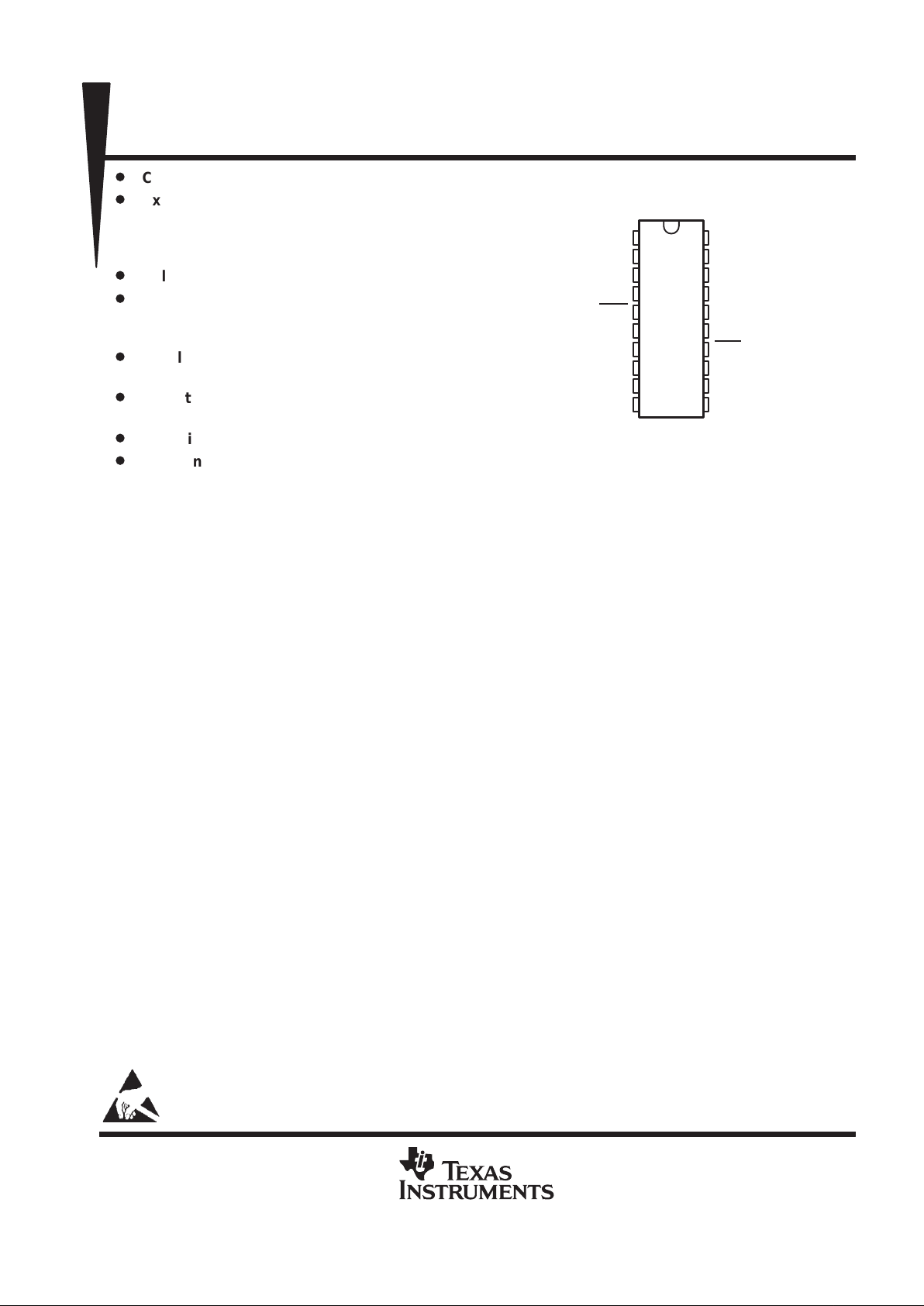
DW OR N PACKAGE
(TOP VIEW)
TCM29C23, TCM129C23
VARIABLE-FREQUENCY PCM OR DSP INTERFACE
SCTS029A – AUGUST 1989 –REVISED JUL Y 1996
2
POST OFFICE BOX 655303 • DALLAS, TEXAS 75265
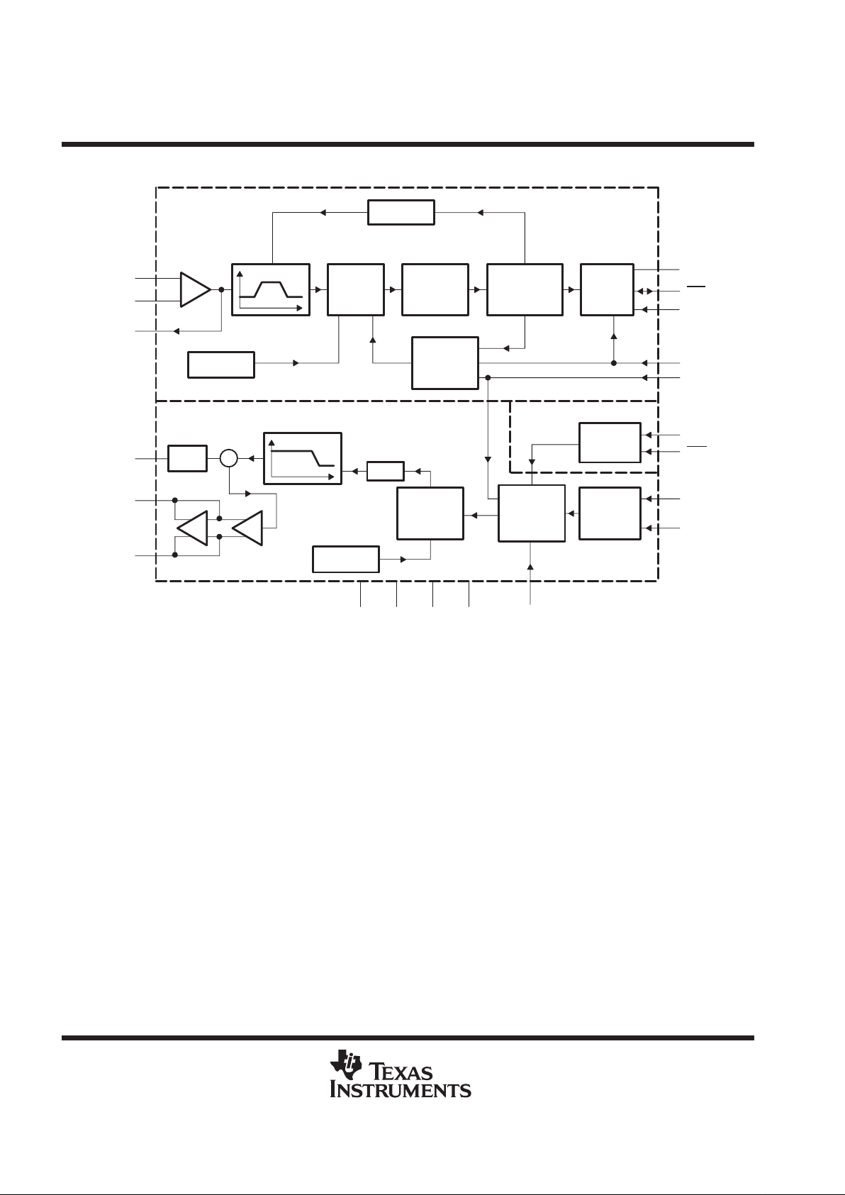
functional block diagram
Buffer
PWRO+
PWRO–
GSX
ANLG IN+
Transmit Section
Receive Section
Control Section
CLKSEL
Control
Logic
DCLKR
PCM IN
Input
Register
Digital-
to-Analog
Control
Logic
Reference
Sample
and Hold
and DAC
Analog-
to-Digital
Control
Logic
Gain
Set
Filter
Reference
FSX/TSXE
Autozero
Output
Register
TSX/DCLKX
PCM OUT
Approximation
Successive
Comparator
Sample
and Hold
and DAC
Filter
Σ
CLKR/CLKX
FSR/TSRE
ANLG
GND
DGTL
GND
V
BB
V
CC
ANLG IN–
SIGX/ASEL
PDN
GSR
13
14
15
12
11
6
5
8
7
17
18
19
4
2
3
20 1 10 16 9
TCM29C23, TCM129C23
VARIABLE-FREQUENCY PCM OR DSP INTERFACE
SCTS029A – AUGUST 1989 –REVISED JUL Y 1996
3
POST OFFICE BOX 655303 • DALLAS, TEXAS 75265
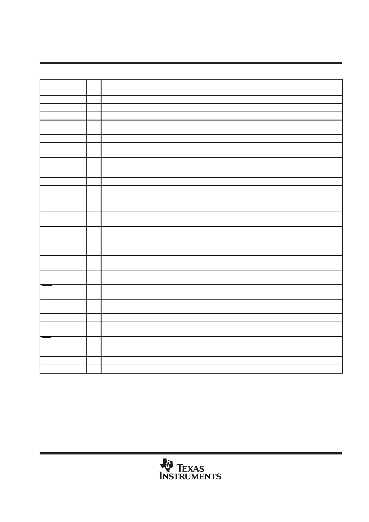
Terminal Functions
TERMINAL
NAME NO.
I/O
DESCRIPTION
ANLG GND 16 Analog ground return for all internal voice circuits. Not internally connected to DGTL GND.
ANLG IN+ 17 I Noninverting analog input to uncommitted transmit operational amplifier.
ANLG IN– 18 I Inverting analog input to uncommitted transmit operational amplifier.
CLKR 11 I Receive master clock and data clock for the fixed-data-rate mode. Receive master clock only for variable-data-rate
mode. CLKR and CLKX are internally connected together.
CLKSEL 6 I Clock frequency selection. Input must be connected to VBB, VCC, or ground to reflect the master clock frequency.
CLKX 11 I Transmit master clock and data clock for the fixed-data-rate mode. Transmit master clock only for
variable-data-rate mode. CLKR and CLKX are internally connected.
DCLKR 7 I Selects fixed- or variable-data-rate operation. When connected to VBB, the device operates in the fixed-data-rate
mode. When DCLKR is not connected to VBB, the device operates in the variable-data-rate mode and DCLKR
becomes the receive data clock, which operates at frequencies from 64 kHz to 4.096 MHz.
DGTL GND 10 Digital ground for all internal logic circuits. Not internally connected to ANLG GND.
FSR/TSRE 9 I Frame-synchronization clock input/time-slot enable for receive channel. In the fixed-data-rate mode, FSR
distinguishes between signaling and nonsignaling frames by a double- or single-length pulse, respectively . In the
variable-data-rate mode, this signal must remain high for the duration of the slot. The receive channel enters the
standby state when FSR is TTL low for 300 ms.
FSX/TSXE 12 I Frame-synchronization clock input/time-slot enable for the transmit channel. Operates independently of, but in an
analogous manner to, FSR/TSRE. The transmit channel enters the standby state when FSX is low for 300 ms.
GSR 4 I Input to the gain-setting network on the output power amplifier. T ransmission level can be adjusted over a 12-dB
range depending upon the voltage at GSR.
GSX 19 O Output terminal of internal uncommitted operational amplifier. Internally , this is the voice signal input to the transmit
filter.
PCM IN 8 I Receive PCM input. PCM data is clocked in on this pin on eight consecutive negative transition of the receive data
clock, which is CLKR in fixed-data-rate timing and DCLKR in variable-data-rate timing.
PCM OUT 13 O Transmit PCM output. PCM data is clocked out of this output on eight consecutive positive transition of the transmit
data clock, which is CLKX in fixed-data-rate timing and DCLKX in variable-data-rate timing.
PDN 5 I Power-down select. This device is inactive with a TTL low-level input to this terminal and active with a TTL high-level
input to this terminal.
PWRO+ 2 O Noninverting output of power amplifier. Can drive transformer hybrids or high-impedance loads directly in either
a differential or single-ended configuration.
PWRO– 3 O Inverting output of power amplifier; functionally identical to but complementary to PWRO+.
SIGX/ASEL 15 I A-law and µ-law operation select. When connected to VBB, A-law is selected. When connected to VCC or ground,
µ-law is selected.
TSX/DCLKX 12 I/O Transmit channel time slot strobe (output) or data clock (input) for the transmit channel. In the fixed-data-rate mode,
this is an open-drain output to be used as an enable signal for a 3-state output buffer. In the variable-data-rate mode,
DCLKX becomes the transmit data clock, which operates at TTL levels from 64 kHz to 2.048 MHz.
V
BB
1 Most negative supply voltage; input is –5 V ±5%.
V
CC
16 Most positive supply voltage; input is 5 V ±5%.
TCM29C23, TCM129C23
VARIABLE-FREQUENCY PCM OR DSP INTERFACE
SCTS029A – AUGUST 1989 –REVISED JUL Y 1996
4
POST OFFICE BOX 655303 • DALLAS, TEXAS 75265
absolute maximum ratings over operating free-air temperature range (unless otherwise noted)
†
Supply voltage range, V
CC
(see Note 1) –0.3 V to 15 V. . . . . . . . . . . . . . . . . . . . . . . . . . . . . . . . . . . . . . . . . . . . .
Output voltage range, V
O
–0.3 V to 15 V. . . . . . . . . . . . . . . . . . . . . . . . . . . . . . . . . . . . . . . . . . . . . . . . . . . . . . . . . .
Input voltage range, V
I
–0.3 V to 15 V. . . . . . . . . . . . . . . . . . . . . . . . . . . . . . . . . . . . . . . . . . . . . . . . . . . . . . . . . . . . .
Digital ground voltage range –0.3 V to 15 V. . . . . . . . . . . . . . . . . . . . . . . . . . . . . . . . . . . . . . . . . . . . . . . . . . . . . . . .
Operating free-air temperature range, T
A
: TCM29C23 0°C to70°C. . . . . . . . . . . . . . . . . . . . . . . . . . . . . . . . . . . .
TCM129C23 –40°C to 85°C. . . . . . . . . . . . . . . . . . . . . . . . . . . . . . . .
Storage temperature range, T
stg
–65°C to 150°C. . . . . . . . . . . . . . . . . . . . . . . . . . . . . . . . . . . . . . . . . . . . . . . . . . .
Lead temperature 1,6 mm (1/16 inch) from case for 10 seconds: DW or N package 260°C. . . . . . . . . . . . . . .
†
Stresses beyond those listed under “absolute maximum ratings” may cause permanent damage to the device. These are stress ratings only, and
functional operation of the device at these or any other conditions beyond those indicated under “recommended operating conditions” is not
implied. Exposure to absolute-maximum-rated conditions for extended periods may affect device reliability.
NOTE 1: Voltage values for maximum ratings are with respect to VBB.
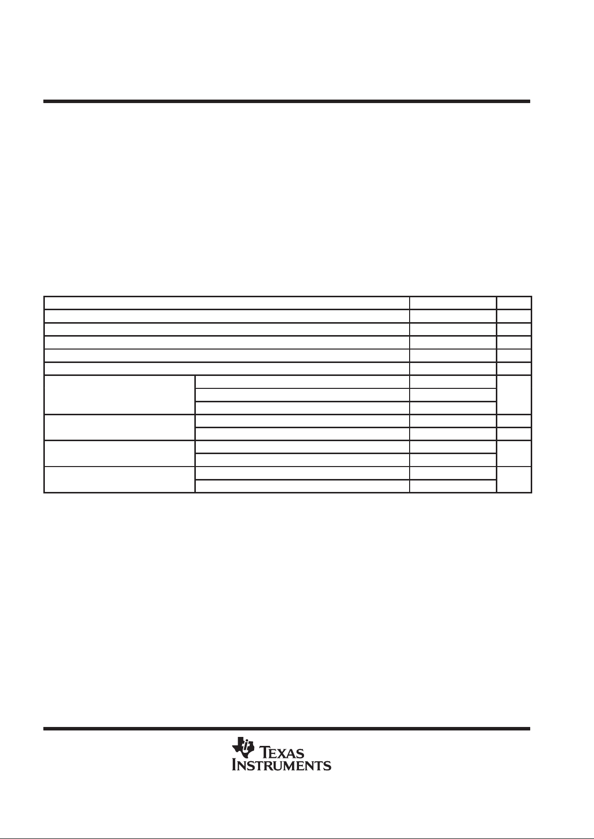
recommended operating conditions (see Note 2)
MIN NOM MAX UNIT
V
CC
Supply voltage (see Note 3) 4.75 5 5.25 V
V
BB
Supply voltage –4.75 –5 –5.25 V
DGTL GND voltage with respect to ANLG GND 0 V
V
IH
High-level input voltage, all inputs except CLKSEL 2.2 V
V
IL
Low-level input voltage, all inputs except CLKSEL 0.8 V
For 2.048 MHz V
BB
VBB +0.5
CLKSEL input voltage
For 1.544 MHz
0 0.5
V
For 1.536 Mhz VCC –0.5 V
CC
At GSX 10 kΩ
RLLoad resistance
At PWRO+ and/or PWRO– 300 Ω
p
At GSX 50
p
CLLoad capacitance
At PWRO+ and/or PWRO– 100
pF
p
p
TCM29C23 0 70
°
TAOperating free-air temperature
TCM129C23 –40 85
°C
NOTES: 2. T o avoid possible damage to these CMOS devices and resulting reliability problems, the power-up procedure described in the device
power-up sequence paragraphs later in this document should be followed.
3. Voltages at analog inputs and outputs, VCC and VBB, are with respect to ANLG GND. All other voltages are referenced to
DGTL GND unless otherwise noted.
TCM29C23, TCM129C23
VARIABLE-FREQUENCY PCM OR DSP INTERFACE
SCTS029A – AUGUST 1989 –REVISED JUL Y 1996
5
POST OFFICE BOX 655303 • DALLAS, TEXAS 75265
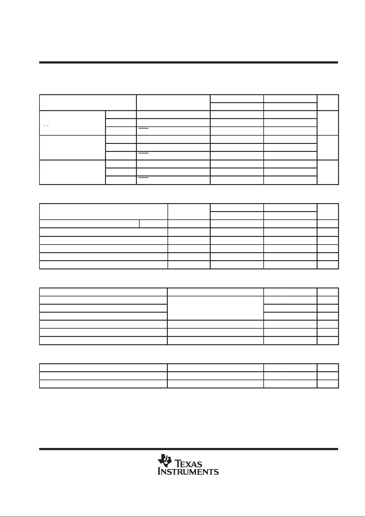
electrical characteristics over recommended ranges of supply voltage and operating free-air
temperature (unless otherwise noted)
supply current, f
DCLK
= 4.096 MHz, outputs not loaded
TCM29C23 TCM129C23
PARAMETER
TEST CONDITIONS
MIN TYP†MAX MIN TYP†MAX
UNIT
Operating 7 9 8 13
I
CC
Supply current from
Standby FSX, or FSR at VIL after 300 ms 0.5 1 0.7 1.5
mA
CC
V
CC
Power down
PDN at VIL after 10 µs
0.3 0.8 0.4 1
Operating –7 –9 –8 –13
I
BB
Supply current from
Standby FSX or FSR at VIL after 300 ms –0.5 –1 –0.7 –1.5
mA
BB
V
BB
Power down
PDN at VIL after 10 µs
–0.3 –0.8 –0.4 –1
Operating 70 90 80 130
PDPower dissipation
Standby FSX or FSR at VIL after 300 ms 5 10 7 15
mW
Power down
PDN at VIL after 10 µs
3 8 4 10
†
All typical values are at VBB = –5 V, VCC = 5 V, and TA = 25°C.
digital interface
TEST
TMC29C23 TMC129C23
PARAMETER
CONDITIONS
MIN TYP†MAX MIN TYP†MAX
UNIT
V
OH
High-level output voltage PCM OUT IOH = –9.6 mA 2.4 2.4 V
V
OL
Low-level output voltage at PCM OUT, TSX, SIG
IOL = 3.2 mA 0.4 0.5 V
I
IH
High-level input current, any digital input VI = 2.2 V to V
CC
10 12 µA
I
IL
Low-level input current, any digital input VI = 0 to 0.8 V 10 12 µA
C
i
Input capacitance 5 10 5 10 pF
C
o
Output capacitance 5 5 pF
†
All typical values are at VBB = –5 V, VCC = 5 V, and TA = 25°C.
transmit amplifier input
PARAMETER TEST CONDITIONS MIN TYP†MAX UNIT
Input current at ANLG IN+, ANLG IN– ±200 nA
Input offset voltage at ANLG IN +, ANLG IN–
VI = –2.17 V to 2.17 V
±25 mV
Common-mode rejection at ANLG IN+, ANLG IN– 55 dB
Open-loop voltage amplification at GSX 5000
Open-loop unity-gain bandwidth at GSX 1 MHz
Input resistance at ANLG IN+, ANLG IN– 10 MΩ
†
All typical values are at VBB = –5 V, VCC = 5 V, and TA = 25°C.
receive filter output
PARAMETER TEST CONDITIONS MIN TYP†MAX UNIT
Output offset voltage at PWRO+, PWRO– (single ended) Relative to ANLG GND 80 mV
Output resistance at PWRO+, PWRO– 1 Ω
†
All typical values are at VBB = –5 V, VCC = 5 V, and TA = 25°C.
TCM29C23, TCM129C23
VARIABLE-FREQUENCY PCM OR DSP INTERFACE
SCTS029A – AUGUST 1989 –REVISED JUL Y 1996
6
POST OFFICE BOX 655303 • DALLAS, TEXAS 75265
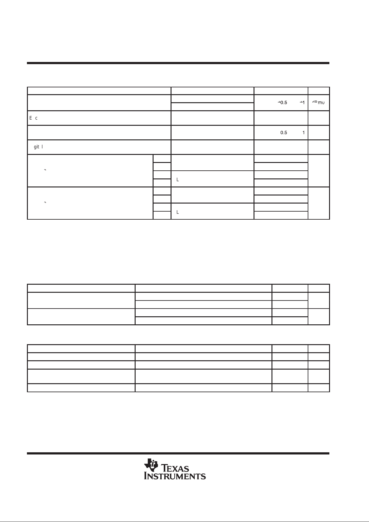
gain and dynamic range, VCC = 5 V, VBB = –5 V, TA = 25°C (unless otherwise noted)
(see Notes 4, 5, and 6)
PARAMETER TEST CONDITIONS MIN TYP MAX UNIT
p
Signal input = 1.064 Vrms for µ-law
Encoder milliwatt response (transmit gain tolerance)
Signal input = 1.068 Vrms for A-law
±
0.5±1
dBm0
Encoder milliwatt response (nominal supplies and temperature)
TA = 0°C to 70°C,
Supply voltages = 5 V ±5%
± 0.15 dB
Digital milliwatt response (receive tolerance gain) relative to
zero-transmission level point
Signal input per CCITT G.711,
Output signal = 1 kHz
±
0.5
±1dBm0
Digital milliwatt response variation with temperature and supplies
TA = 0°C to 70°C,
Supply voltages = 5 V ±5%
± 0.15 dB
µ-law
2.76
p
A-law
R
L
=
600 Ω
2.79
Zero-transmission-level point, transmit channel (0 dBm0)
µ-law
1
dBm
A-law
R
L
=
900 Ω
1.03
µ-law
5.76
p
A-law
R
L
=
600 Ω
5.79
Zero-transmission-level point, receive channel (0 dBm0)
µ-law
4
dBm
A-law
R
L
=
900 Ω
4.03
NOTES: 4. Unless otherwise noted, the analog input is a 0-dBm0, 1020-Hz sine wave, where 0 dBm0 is defined as the zero-reference point of
the channel under test. This corresponds to an analog signal input of 1.064 Vrms or an output of 1.503 Vrms.
5. The input amplifier is set for noninverting unity gain. The digital input is a PCM bit stream generated by passing a 0-dBm0, 1020-Hz
sine wave through an ideal encoder.
6. Receive output is measured single ended in the maximum gain configuration. To set the output amplifier for maximum gain, GSR is
connected to PWRO– and the output is taken at PWRO+. All output levels are (sin x)/x corrected.
gain tracking over recommended ranges of supply voltage and operating free-air temperature,
reference level = –10 dBm0
PARAMETER TEST CONDITIONS MIN MAX UNIT
p
3 ≥ input level ≥ –40 dBm0 ±0.5
Transmit gain-tracking error, sinusoidal input
–40 > input level ≥ –50 dBm0 ±1.5
dB
p
3 ≥ input level ≥ –40 dBm0 ±0.5
Receive gain-tracking error, sinusoidal input
–40 > input level ≥ –50 dBm0 ±1.5
dB
noise over recommended ranges of supply voltage and operating free-air temperature range
PARAMETER TEST CONDITIONS MIN MAX UNIT
Transmit noise, C-message weighted ANLG IN+ = ANLG GND, ANLG IN– = GSX 18 dBrnC0
Transmit noise, psophometrically weighted ANLG IN+ = ANLG GND, ANLG IN– = GSX –72 dBm0p
Receive noise, C-message-weighted quiet code
PCM IN = 11111111 (µ-law), PCM IN = 10101010 (A-law),
Measured at PWRO+
11 dBrnC0
Receive noise, psophometrically weighted PCM = lowest positive decode level –79 dBm0p
 Loading...