


TC213 1024- ×512-PIXEL CCD IMAGE SENSOR
SOCS013B ± AUGUST 1989 ± REVISED DECEMBER 1991
• High-Resolution, Solid-State |
|
|
|
|
DUAL-IN-LINE PACKAGE |
|
|
|||||||||
Frame-Transfer Image Sensor |
|
|
|
|
|
(TOP VIEW) |
|
|
||||||||
• 13.5-mm Image-Area Diagonal |
OUT1 |
|
1 |
|
|
|
|
|
|
|
|
|
|
24 |
|
ABGS |
• 1000 (H) × 510 (V) Active Elements in |
|
|
|
|
|
|
|
|||||||||
|
|
|
|
|
|
|
|
|
|
|
|
|
|
|
|
|
|
|
|
|
|
|
|
|
|
|
|
|
|
|
|
|
|
AMP GND |
|
2 |
23 |
|
SAG |
|||||||||||
|
|
|||||||||||||||
Image-Sensing Area |
|
|
||||||||||||||
|
|
|
|
|
|
|
|
|
|
|
|
|
|
|
|
|
• Square Pixels |
OUT2 |
|
3 |
|
|
|
|
|
|
|
|
|
22 |
|
ABGI |
|
|
|
|
|
|
|
|
|
|
|
|
||||||
• Low Dark Current |
ADB |
|
4 |
|
|
|
|
|
|
|
|
|
21 |
|
IAG |
|
|
|
|||||||||||||||
• Electron-Hole Recombination Antiblooming |
SUB |
|
5 |
|
|
|
|
|
|
|
|
|
20 |
|
SUB |
|
|
|
|||||||||||||||
• Dynamic Range . . . More Than 60 dB |
RST2 |
|
6 |
|
|
|
|
|
|
|
|
|
19 |
|
TDB |
|
|
|
|||||||||||||||
• High Sensitivity |
RST1 |
|
7 |
|
|
|
|
|
|
|
|
|
18 |
|
SUB |
|
|
|
|||||||||||||||
• High Photoresponse Uniformity |
CDB |
|
8 |
|
|
|
|
|
|
|
|
|
17 |
|
SUB |
|
|
|
|
|
|
|
|
|
|
|
|
||||||
|
|
|||||||||||||||
• High Blue Response |
SRG1 |
|
9 |
|
|
|
|
|
|
|
|
|
16 |
|
IAG |
|
|
|
|
|
|
|
|
|
|
|
|
||||||
|
|
|||||||||||||||
• Single-Phase Clocking |
SRG2 |
|
10 |
|
|
|
|
|
|
|
|
|
15 |
|
ABGI |
|
|
|
|
|
|
|
|
|
|
|
|
||||||
|
|
|
|
|
|
|
|
|
|
|
||||||
|
|
|||||||||||||||
• Solid-State Reliability With No Image |
|
|
|
|
|
|
|
|
|
|
|
|
|
|
|
|
|
|
|
|
|
|
|
|
|
|
|
|
|
|
|
|
|
TRG |
|
11 |
14 |
|
SAG |
|||||||||||
Burn-in, Residual Imaging, Image |
|
|
||||||||||||||
IDB |
|
12 |
|
|
|
|
|
|
|
|
|
|
13 |
|
ABGS |
|
Distortion, Image Lag, or Microphonics |
|
|
|
|
|
|
|
|
|
|||||||
|
|
|
|
|
|
|
|
|
|
|
|
|
|
|
|
|
|
|
|
|
|
|
|
|
|
|
|
|
|
|
|
|
|
description
The TC213 is a frame-transfer charge-coupled device (CCD) image sensor that provides very high-resolution image acquisition for image-processing applications such as robotic vision, medical X-ray analysis, and metrology. The image format measures 12.00 mm horizontally by 6.12 mm vertically; the image-area diagonal is 13.5 mm. The image-area pixels are 12-mm square. The image area contains 510 active lines with 1000 active pixels per line. Two additional dark reference lines give a total of 512 lines in the image area, and 24 additional dark-reference pixels per line give a total of 1024 pixels per horizontal line.
The storage section of the TC213 contains 512 lines with 1024 pixels per line. This area is protected from exposure to light by an aluminum light shield. Photoelectric charge that is generated in the image area of the TC213 can be transferred into the storage section in less than 500 ms. After image capture (integration time), the readout is accomplished by transferring the charge, one line at a time, into two serial registers located below the storage area, each of which contains 512 data elements and 12 dummy elements. One serial-register clocks out charge that is generated in the odd-numbered columns of pixels in the imaging area; the other serial-register processes charge from the even-numbered columns of the imaging area. The typical serial-register data rate is 10 megapixels per second. Three transfer gates are used to isolate the serial registers. If the storage area or storage and image areas need to be cleared of all charge, charge may be quickly transferred across the serial registers and into the clearing drain, which is located below the serial-register section.
This MOS device contains limited built-in gate protection. During storage or handling, the device leads should be shorted together or the device should be placed in conductive foam. In a circuit, unused inputs should always be connected to SUB. Under no circumstances should pin voltages exceed absolute maximum ratings. Avoid shorting OUTn to ADB during operation to prevent damage to the amplifier. The device can also be damaged if the output terminals are reverse-biased and an excessive current is
allowed to flow. Specific guidelines for handling devices of this type are contained in the publication Guidelines for Handling Electrostatic-Discharge-Sensitive (ESDS) Devices and Assemblies available from Texas Instruments.
PRODUCTION DATA information is current as of publication date. Products conform to specifications per the terms of Texas Instruments standard warranty. Production processing does not necessarily include testing of all parameters.
Copyright 1991, Texas Instruments Incorporated
POST OFFICE BOX 655303 •DALLAS, TEXAS 75265 |
2-1 |
TC213
1024- ×512-PIXEL CCD IMAGE SENSOR
SOCS013B ± AUGUST 1989 ± REVISED DECEMBER 1991
description (continued)
Gated floating-diffusion detection structures are used with each serial register to convert charge to signal voltage. External resets allow the application of off-chip correlated clamp sample-and-hold amplifiers for low-noise performance. To provide high output-drive capability, both outputs are buffered by low-noise, two-stage, source-follower amplifiers. These two output signals can provide a data rate of 20 megapixels per second when combined off chip. An output of 30 frames per second with one field per frame is typical. At room temperature, the readout noise is 55 elecrons and a minimum dynamic range of 60 dB is available.
The blooming protection incorporated into the sensor is based on recombining excess charge with charge of opposite polarity in the substrate. This antiblooming is activated by supplying clocking pulses to the antiblooming gate, which is an integral part of each image-sensing element. The storage area antiblooming gate is clocked only for charge transfer in normal use.
The TC213 is built using TI-proprietary virtual-phase technology, which provides devices with high blue response, low dark signal, good uniformity, and single-phase clocking.
The TC213 is characterized for operation from ±10°C to 40°C.
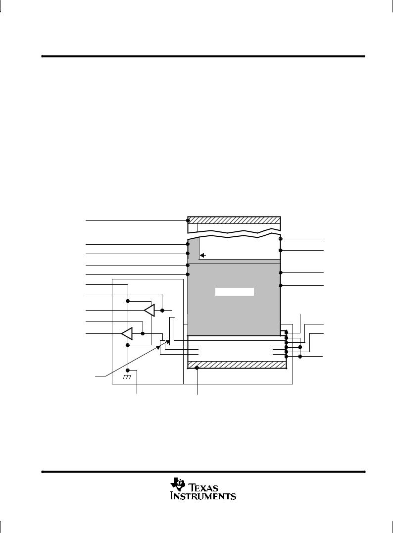
functional block diagram
Top Drain
TDB |
19 |
|
|
|
|
||
IAG |
21 |
|
|
22 |
|
||
ABGI |
|
||
|
|
||
SAG |
23 |
|
|
24 |
|
||
ABGS |
|
||
4 |
|
||
ADB |
Amplifiers |
||
|
|||
6 |
|
||
RST2 |
|
||
|
|
||
OUT2 |
3 |
|
|
|
|
||
RST1 |
7 |
|
|
|
|
||
OUT1 |
1 |
|
|
|
|
||
12 Dummy |
|
||
Elements |
|
|
|
|
|
2 |
|
AMP GND
|
|
16 |
Image Area With |
|
IAG |
|
15 |
|
Blooming Protection |
|
|
24 Dark Reference Elements |
|
ABGI |
|
|
|
|
|
14 |
|
|
SAG |
|
|
13 |
Storage Area |
|
ABGS |
|
|
|
|
IDB |
|
|
12 |
10 |
|
|
|
|
|
SRG2 |
|
|
9 |
|
|
SRG1 |
Multiplexer, Transfer Gates, |
|
|
and Serial Registers |
|
11 |
|
|
TRG |
Clearing Drain |
|
|
8 |
|
|
CDB |
|
|
2-2 |
POST OFFICE BOX 655303 •DALLAS, TEXAS 75265 |

TC213 1024- ×512-PIXEL CCD IMAGE SENSOR
SOCS013B ± AUGUST 1989 ± REVISED DECEMBER 1991
sensor topology diagram
|
|
|
|
|
|
|
|
|
|
|
|
|
|
|
|
|
|
|
|
|
|
|
|
|
|
|
|
|
|
|
|
|
|
|
|
|
|
|
|
|
|
|
|
1000 Pixels |
|
|
|
|
|
|
|
|
|
|
|
|
|
|
|
|
|
|
|
|
|
|
|
|
|
|
|
|
|
|
|
|
|
|
|
|
|
|
|
|
|
|
|
|
510 Lines |
|
||||
|
|
|
|
|
22 Pixels |
|
|
|
|
|
|
|
|
|||||
|
|
|
|
|
|
|
|
|
|
|
|
|
|
|
|
|
||
|
|
|
|
|
|
|
|
|
|
|
|
|
|
|
|
|
||
|
|
|
|
|
1 Pixel |
1 Pixel |
|
|
|
|
|
|
|
|
2 Lines |
|||
|
|
|
|
|
|
|
|
|
|
|
|
|
||||||
|
|
|
|
|
|
|
|
|
|
|
|
|
|
|
|
|||
|
|
|
|
|
|
|
|
|
|
|
|
|
|
|
|
|
|
|
|
|
|
|
|
|
|
|
|
|
|
|
|
|
|
|
|
|
|
|
|
|
|
|
|
|
|
|
|
|
|
|
|
|
|
|
|
|
|
|
|
|
|
|
|
|
|
|
|
|
|
|
|
|
|
|
|
512 Lines
Dummy Pixels
|
|
|
|
|
|
|
|
|
12 |
|
|
511 |
|
||
|
|
|
|
|
|
|
|
|
|
|
|
|
|
||
|
|
|
|
|
|
|
|
|
12 |
|
511 |
|
|||
|
|
|
|
|
|
|
|
Terminal Functions
TERMINAL |
I/O |
DESCRIPTION |
||
NAME |
NO. |
|||
|
|
|||
|
|
|
|
|
ABGI² |
15 |
I |
Antiblooming gate for image area |
|
ABGI² |
22 |
I |
Antiblooming gate for image area |
|
ABGS² |
13 |
I |
Antiblooming gate for storage area |
|
ABGS² |
24 |
I |
Antiblooming gate for storage area |
|
ADB |
4 |
I |
Supply voltage for amplifier drain bias |
|
|
|
|
|
|
AMP GND |
2 |
|
Amplifier ground |
|
|
|
|
|
|
CDB |
8 |
I |
Supply voltage for clearing drain bias |
|
|
|
|
|
|
IAG² |
16 |
I |
Image-area gate |
|
IAG² |
21 |
I |
Image-area gate |
|
IDB |
12 |
I |
Supply voltage for input diode bias |
|
|
|
|
|
|
OUT1 |
1 |
O |
Output signal 1 |
|
|
|
|
|
|
OUT2 |
3 |
O |
Output signal 2 |
|
|
|
|
|
|
RST1 |
7 |
I |
Reset gate 1 |
|
|
|
|
|
|
RST2 |
6 |
I |
Reset gate 2 |
|
|
|
|
|
|
SAG² |
14 |
I |
Storage-area gate |
|
SAG² |
23 |
I |
Storage-area gate |
|
SRG1 |
9 |
I |
Serial-register gate 1 |
|
|
|
|
|
|
SRG2 |
10 |
I |
Serial-register gate 2 |
|
|
|
|
|
|
SUB² |
5 |
|
Substrate and clock return |
|
SUB² |
17 |
|
Substrate and clock return |
|
SUB² |
18 |
|
Substrate and clock return |
|
SUB² |
20 |
|
Substrate and clock return |
|
TDB |
19 |
I |
Supply voltage for top drain bias |
|
|
|
|
|
|
TRG |
11 |
I |
Transfer gate |
|
²All pins of the same name should be connected together externally (i.e., pin 15 to pin 22, pin 13 to pin 24, etc.).
POST OFFICE BOX 655303 •DALLAS, TEXAS 75265 |
2-3 |

TC213
1024- ×512-PIXEL CCD IMAGE SENSOR
SOCS013B ± AUGUST 1989 ± REVISED DECEMBER 1991
detailed description
The TC213 consists of four basic functional blocks: (1) the image-sensing area, (2) the image-storage area,
(3) the multiplexer block with serial registers and transfer gates, and (4) the low-noise signal-processing amplifier block with charge-detection nodes. The location of each of these blocks is identified in the functional block diagram.
image-sensing and image-storage areas
Figures 1 and 2 show cross sections with potential well diagrams and top views of image-sensing elements. As light enters the silicon in the image-sensing area, free electrons are generated and collected in the potential wells of the sensing elements. During this time, blooming protection is activated by applying a burst of pulses to the antiblooming gate inputs every horizontal blanking interval. This prevents blooming caused by the spilling of charge from overexposed elements into neighboring elements. After integration is complete, the signal charge is transferred into the storage area (see Figure 5).
There are 24 full columns of elements at the left edge of the image-sensing area that are shielded from incident light; these elements provide the dark reference used in subsequent video-processing circuits to restore the video black level. There are also two dark lines at the bottom of the image-sensing area that prevent charge leakage from the image-sensing area into the image-storage area.
multiplexer with transfer gates and serial registers
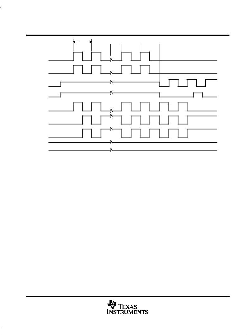
The multiplexer and transfer gates transfer charge line by line from the image-storage area columns into the corresponding serial registers and prepare it for readout. Figure 3 illustrates the layout of the multiplexing gate that vertically separates the pixels for input into the serial registers. Figure 4 shows the layout of the interface region between the serial-register gates and the transfer gates. Multiplexing is activated during the horizontal blanking interval by applying appropriate pulses to the transfer gates and serial registers; the required pulse timing is shown in Figure 6. A drain is also included to provide the capability to clear the image-sensing area of unwanted charge. Such charge can accumulate in the imager during the start-up of operation or under special circumstances when nonstandard timing is desired. The clear timing is given as part of the parallel-transfer timing in Figure 5.
serial-register readout and video processing
After transfer into the serial registers, the pixels are normally read out 180° out of phase (see Figure 7). Each serial register must be reset to the reference level before the next pixel is read out. The timing for the resets and their relationships to the serial-register pulses is shown in Figure 8. Figure 8 also shows the timing for the pixel clamp and sample and hold needed for an off-chip double-correlated sampling circuit. These two output signals can provide a data rate of 20 million pixels per second when combined off chip. After the charge is placed on the detection node, it is buffered and amplified by a low-noise, dual-stage source follower. Each serial register contains 12 dummy elements that are used to span the distance between the serial register and the output amplifier. A schematic is shown in Figure 9. The location of the dummy elements, which are considered to be part of the amplifiers, is shown in the functional block diagram. Figure 10 gives the timing for a single frame of video. An output of 30 frames per second with one field per frame is typical.
2-4 |
POST OFFICE BOX 655303 •DALLAS, TEXAS 75265 |

TC213 1024- ×512-PIXEL CCD IMAGE SENSOR
SOCS013B ± AUGUST 1989 ± REVISED DECEMBER 1991
μ |
Clocked Barrier |
|
Light |
12 m(H) |
|
|
|
|
|
φ-IAG |
φ-ABG |
12 μm(V) |
Virtual Barrier |
Antiblooming |
|
Antiblooming Gate |
Clocking Levels |
|
|
|
|
||
|
|
|
|
|
Virtual Well |
|
|
|
Clocked Well |
Accumulated Charge |
|
|
|
|
Figure 1. Charge-Accumulation Process
φ-PS
 Clocked Phase
Virtual Phase
Channel Stops
Figure 2. Charge-Transfer Process
Channel Stops
Channel |
|
Serial- |
|
|
Register |
||
Stop |
Clocked |
||
Gate |
|||
Virtual |
|||
Wells |
|
||
Well |
|
|
|
Clocked |
|
|
|
Well Multiplexing |
|
|
|
Gate |
|
|
Transfer
Gate
Figure 3. Multiplexing-Gate Layout |
Figure 4. Interface-Region Layout |
|
|
|
|
POST OFFICE BOX 655303 •DALLAS, TEXAS 75265 |
2-5 |
TC213
1024- ×512-PIXEL CCD IMAGE SENSOR
SOCS013B ± AUGUST 1989 ± REVISED DECEMBER 1991
1 μs |
|
|
Line 1 |
Line 2 |
Line 511 Line 512 |
IAG |
|
|
SAG |
|
|
Intermediate |
High |
|
|
||
ABGI |
|
Low |
|
|
|
Intermediate |
|
|
ABGS |
|
|
TRG
SRG1²
SRG2²
RST1
High
RST2
High
²SRG1 and SRG2 pulses are extended to equal TRG and SAG pulse widths during parallel transfers from the storage area to the clearing drain.
Figure 5. Parallel-Transfer Timing
2-6 |
POST OFFICE BOX 655303 •DALLAS, TEXAS 75265 |

TC213 1024- ×512-PIXEL CCD IMAGE SENSOR
SOCS013B ± AUGUST 1989 ± REVISED DECEMBER 1991
CSYNC
CBLNK
TRG
SRG1²
SRG2²
RST1 High
RST2 High
CL1 Low
CL2 Low
SH1 Low
SH2 Low
SAG
ABGS |
|
|
Intermediate |
|
|
||
|
|
|
|
ABGI
CPOB1
CPOB2
IAG Low
² SRG1 and SRG2 pulses are extended to equal TRG and SAG pulse widths during horizontal line transfer operation for readout.
Figure 6. Horizontal Timing
POST OFFICE BOX 655303 •DALLAS, TEXAS 75265 |
2-7 |
 Loading...