Texas Instruments THS1050EVM, THS1050IPHP, THS1050CPHP Datasheet
THS1050 10-BIT 50 MSPS IF SAMPLING COMMUNICATIONS ANALOG-TO-DIGITAL CONVERTER
SLAS278 ± APRIL 2000
features |
applications |
||
D 50 MSPS Maximum Sample Rate |
D |
Wireless Local Loop |
|
D |
10-Bit Resolution |
D |
Wireless Internet Access |
D |
No Missing Codes |
D |
Cable Modem Receivers |
D On-Chip Sample and Hold |
D |
Medical Ultrasound |
|
D 73 dB Spurious Free Dynamic Range at |
D |
Magnetic Resonant Imaging |
|
fin = 15.5 MHz
D 5 V Analog and Digital Supply |
|
|
|
|
|
|
|
|
|
|
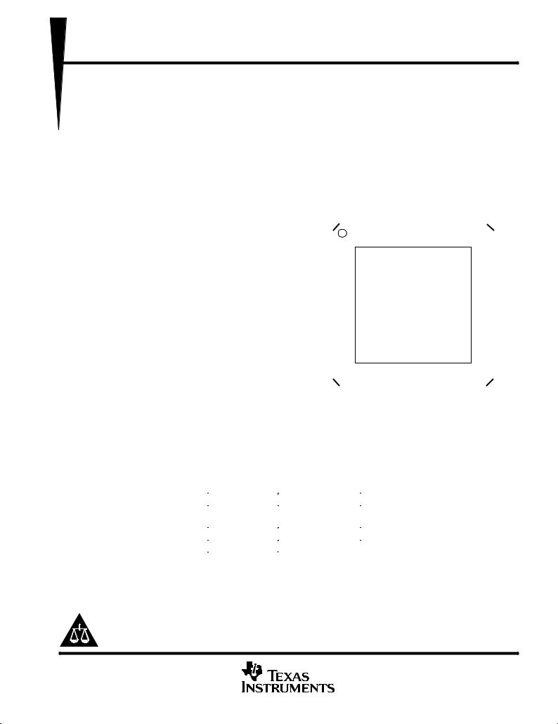
48 PHP PACKAGE |
|
|
|
|
|
|
|
|
|
|
|||||||||||
|
|
|
|
|
|
|
|
|
|
|
|
(TOP VIEW) |
|
|
|
|
|
|
|
|
|
|
|
|
||||||||
D 3 V and 5 V CMOS Compatible Digital |
|
|
|
|
|
|
|
|
|
|
|
|
|
|
|
|
|
|
|
|
|
|
|
|
||||||||
|
|
|
|
|
|
|
|
|
|
|
|
|
|
|
|
|
|
|
|
SS |
SS |
DD |
DD |
|
|
|||||||
Output |
|
|
|
|
CM |
|
DD |
SS |
DD |
SS |
DD |
SS |
SS |
|
|
|||||||||||||||||
D 9.7 Bit ENOB at fIN = 31 MHz |
|
|
|
|
|
|
|
|||||||||||||||||||||||||
|
|
|
|
V |
|
AV |
AV |
AV |
AV |
AV |
AV |
AV |
DRV |
DRV |
DRV |
DRV |
|
|
||||||||||||||
D 60 dB SNR at fIN = 31 MHz |
|
|
|
|
|
|
|
|||||||||||||||||||||||||
|
|
|
|
|
|
|
|
|
|
|
|
|
|
|
|
|
|
|
|
|
|
|
|
|
|
|
|
|
|
|
|
|
|
|
48 47 46 45 44 43 42 41 40 39 38 37 |
|
|
|
|
|
|||||||||||||||||||||||||
D 82 MHz Bandwidth |
AVSS |
|
|
|
|
|
NC |
|||||||||||||||||||||||||
|
1 |
|
|
|
|
|
|
|
|
|
|
|
|
|
|
|
|
|
|
|
|
|
|
36 |
|
|||||||
D Internal or External Reference |
|
|
|
|
|
|
|
|
|
|
|
|
|
|
|
|
|
|
|
|
|
|
|
|
||||||||
|
|
|
|
|
|
|
|
|
|
|
|
|
|
|
|
|
|
|
|
|
|
|
|
|
|
|
|
NC |
||||
AVDD |
|
2 |
|
|
|
|
|
|
|
|
|
|
|
|
|
|
|
|
|
|
|
|
|
|
35 |
|
||||||
D Buffered 900 Ω Differential Analog Input |
|
|
|
|
|
|
|
|
|
|
|
|
|
|
|
|
|
|
|
|
|
|
|
|
||||||||
|
|
|
|
|
|
|
|
|
|
|
|
|
|
|
|
|
|
|
|
|
|
|
|
|
|
|
|
D0 |
||||
VIN+ |
|
3 |
|
|
|
|
|
|
|
|
|
|
|
|
|
|
|
|
|
|
|
|
|
|
34 |
|
||||||
|
|
|
|
|
|
|
|
|
|
|
|
|
|
|
|
|
|
|
|
|
|
|
|
|
|
|
|
|
D1 |
|||
description |
VIN± |
|
4 |
|
|
|
|
|
|
|
|
|
|
|
|
|
|
|
|
|
|
|
|
|
|
33 |
|
|||||
|
|
|
|
|
|
|
|
|
|
|
|
|
|
|
|
|
|
|
|
|
|
|
|
|
|
|
|
D2 |
||||
AVDD |
|
5 |
|
|
|
|
|
|
|
|
|
|
|
|
|
|
|
|
|
|
|
|
|
|
32 |
|
||||||
|
|
|
|
|
|
|
|
|
|
|
|
|
|
|
|
|
|
|
|
|
|
|
|
|
||||||||
|
|
|
|
|
|
|
|
|
|
|
|
|
|
|
|
|
|
|
|
|
|
|
|
|
|
|
|
|
D3 |
|||
The THS1050 is a high speed low noise 10-bit |
VREFOUT± |
|
6 |
|
|
|
|
|
|
|
|
|
|
|
|
|
|
|
|
|
|
|
|
|
|
31 |
|
|||||
|
|
|
|
|
|
|
|
|
|
|
|
|
|
|
|
|
|
|
|
|
|
|
|
|
|
|
|
D4 |
||||
CMOS pipelined analog-to-digital converter. A |
VREFIN± |
|
7 |
|
|
|
|
|
|
|
|
|
|
|
|
|
|
|
|
|
|
|
|
|
|
30 |
|
|||||
|
|
|
|
|
|
|
|
|
|
|
|
|
|
|
|
|
|
|
|
|
|
|
|
|
|
|
|
D5 |
||||
differential sample and hold minimizes even order |
VREFIN+ |
|
8 |
|
|
|
|
|
|
|
|
|
|
|
|
|
|
|
|
|
|
|
|
|
|
29 |
|
|||||
|
|
|
|
|
|
|
|
|
|
|
|
|
|
|
|
|
|
|
|
|
|
|
|
|
|
|
|
D6 |
||||
harmonics and allows for a high degree of VREFOUT+ |
|
9 |
|
|
|
|
|
|
|
|
|
|
|
|
|
|
|
|
|
|
|
|
|
|
28 |
|
||||||
|
|
|
|
|
|
|
|
|
|
|
|
|
|
|
|
|
|
|
|
|
|
|
|
|
|
|
|
D7 |
||||
common mode rejection at the analog input. A |
VBG |
|
10 |
|
|
|
|
|
|
|
|
|
|
|
|
|
|
|
|
|
|
|
|
|
|
27 |
|
|||||
|
|
|
|
|
|
|
|
|
|
|
|
|
|
|
|
|
|
|
|
|
|
|
|
|
|
|
|
D8 |
||||
buffered analog input enables operation with a |
AVSS |
|
11 |
|
|
|
|
|
|
|
|
|
|
|
|
|
|
|
|
|
|
|
|
|
|
26 |
|
|||||
|
|
|
|
|
|
|
|
|
|
|
|
|
|
|
|
|
|
|
|
|
|
|
|
|
|
|
|
D9 |
||||
constant analog input impedance, and prevents |
AVDD |
|
12 |
|
|
|
|
|
|
|
|
|
|
|
|
|
|
|
|
|
|
|
|
|
|
25 |
|
|||||
|
|
|
|
|
|
|
|
|
|
|
|
|
|
|
|
|
|
|
|
|
|
|
|
|
|
|
|
|
|
|
||
transient voltage spikes from feeding backward to |
|
|
13 14 15 16 17 18 19 20 21 22 23 24 |
|
|
|
|
|
||||||||||||||||||||||||
|
|
|
|
|
|
|||||||||||||||||||||||||||
the analog input source. Full temperature DNL |
|
|
|
|
|
|
|
|
|
|
|
|
|
|
|
|
|
|
|
|
|
|
|
|
|
|
|
|
|
|
|
|
|
|
|
|
SS |
|
SS |
CLK+ |
CLK± |
DD |
SS |
SS |
DD |
SS |
DD |
SS |
DD |
|
|
||||||||||||||
performance allows for industrial application with |
|
|
|
|
|
|
|
|||||||||||||||||||||||||
the assurance of no missing codes. The typical |
|
|
|
AV |
|
DV |
DV |
DV |
DV |
DV |
DV |
DV |
DRV |
DRV |
|
|
||||||||||||||||
integral nonlinearity (INL) for the THS1050 is less |
|
|
|
|
|
|
||||||||||||||||||||||||||
|
|
|
|
|
|
|
|
|
|
|
|
|
|
|
|
|
|
|
|
|
|
|
|
|
|
|
|
|
|
|
|
|
than one LSB. The superior INL curve of the THS1050 results in SFDR performance that is exceptional for a 10-bit analog-to-digital converter. The THS1050 can operate with either internal or external references. Internal reference usage selection is accomplished simply by externally connecting reference output terminals to reference input terminals.
AVAILABLE OPTIONS
|
PACKAGE |
TA |
|
48-TQFP |
|
|
(PHP) |
|
|
± 40°C to 85°C |
THS1050I |
|
|
0°C to 70°C |
THS1050C |
Please be aware that an important notice concerning availability, standard warranty, and use in critical applications of Texas Instruments semiconductor products and disclaimers thereto appears at the end of this data sheet.
PRODUCTION DATA information is current as of publication date. Products conform to specifications per the terms of Texas Instruments standard warranty. Production processing does not necessarily include testing of all parameters.
Copyright 2000, Texas Instruments Incorporated
POST OFFICE BOX 655303 •DALLAS, TEXAS 75265 |
1 |
THS1050
10-BIT 50 MSPS IF SAMPLING COMMUNICATIONS ANALOG-TO-DIGITAL CONVERTER
SLAS278 ± APRIL 2000
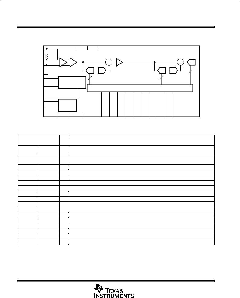
functional block diagram
|
|
|
AVDD DVDD DRVDD |
|
|
|
|
|
|
|
|
|
|
|
||
VIN+ |
|
|
|
|
|
Stage 1 |
|
Stages 2 ± 9 |
Stage 10 |
|
|
|||||
|
Buffer |
|
|
|
|
|
|
|||||||||
|
|
|
|
|
|
|
|
|
|
|
|
|
|
|
||
|
900 Ω |
|
|
S/H |
|
Σ |
|
|
|
|
|
|
|
|
Σ |
|
VIN± |
|
|
|
|
|
|
|
|
|
|
|
|
A/D |
|||
|
|
|
|
|
|
|
|
|
|
|
|
|
|
|||
|
|
|
|
|
|
|
|
|
|
|
|
|
|
|
||
|
|
|
|
|
|
|
|
|
|
|
|
|
|
|
|
|
|
|
|
|
A/D |
D/A |
|
|
|
|
|
|
|
A/D |
D/A |
|
1 |
VREFIN+ |
|
|
|
|
|
|
|
|
|
|
|
|
|
|
|
|
|
|
|
|
|
|
|
|
|
|
|
|
|
|
|
|
|
VREFOUT+ |
3.0 V |
|
1 |
|
|
|
|
|
|
|
|
1 |
|
|
|
|
|
|
Reference |
|
|
|
|
|
|
|
|
|
|
|
|
||
VREFOUT± |
2.0 V |
AVDD/2 |
|
|
|
Digital Error Correction |
|
|
|
|
||||||
VREFIN± |
|
|
|
|
|
|
|
|
|
|
|
|||||
|
|
|
|
|
|
|
|
|
|
|
|
|
|
|
|
|
VCM |
|
|
|
|
|
|
|
|
|
|
|
|
|
|
|
|
CLK+ |
|
|
|
|
|
|
|
|
|
|
|
|
|
|
|
|
CLK± |
Timing |
|
|
|
|
|
|
|
|
|
|
|
|
|
||
|
|
|
|
|
|
|
|
|
|
|
|
|
|
|
|
|
|
AVSS |
DVSS |
DRVSS |
D9 |
D8 |
D7 |
D6 |
D5 |
D4 |
D3 |
D2 |
D1 |
D0 |
|
|
|
|
|
|
Terminal Functions |
|
TERMINAL |
I/O |
DESCRIPTION |
||
NAME |
NO. |
|||
|
|
|||
AVDD |
2, 5, 12 43, |
I |
Analog power supply |
|
|
45, 47 |
|
|
|
AVSS |
1, 11, 13, 41, |
I |
Analog ground return for internal analog circuitry |
|
|
42, 44, 46 |
|
|
|
CLK+ |
15 |
I |
Clock input |
|
CLK± |
16 |
I |
Complementary clock input |
|
D9±D0 |
25±34 |
O |
Digital data output bits; LSB= D0, MSB = D9 (2s complement output format) |
|
DRVDD |
24, 37, 38 |
I |
Digital output driver supply |
|
DRVSS |
23, 39, 40 |
I |
Digital output driver ground return |
|
DVDD |
17, 20, 22 |
I |
Positive digital supply |
|
DVSS |
18, 19, 21 |
I |
Digital ground return |
|
VBG |
10 |
O |
Band gap reference. Bypass to ground with a 1 µF and a 0.01 µF chip capacitor. |
|
VCM |
48 |
O |
Common mode voltage output. Bypass to ground with a 0.1 µF and a 0.01 µF chip device capacitor. |
|
VIN+ |
3 |
I |
Analog signal input |
|
VIN± |
4 |
I |
Complementary analog signal input |
|
VREFIN ± |
7 |
I |
External reference input low |
|
VREFIN+ |
8 |
I |
External reference input high |
|
VREFOUT+ |
9 |
O |
Internal reference output. Compensate with a 1 µF and a 0.01 µF chip capacitor. |
|
VREFOUT ± |
6 |
O |
Internal reference output. Compensate with a 1 µF and a 0.01 µF chip capacitor. |
|
2 |
POST OFFICE BOX 655303 •DALLAS, TEXAS 75265 |

THS1050 10-BIT 50 MSPS IF SAMPLING COMMUNICATIONS ANALOG-TO-DIGITAL CONVERTER
SLAS278 ± APRIL 2000
detailed description
The THS1050 uses a differential pipeline architecture and assures no missing codes over the full operating temperature range. The device uses a 1 bit per stage architecture in order to achieve the highest possible bandwidth. The differential analog inputs are terminated with a 900-Ω resistor. The inputs are then fed to a unity gain buffer followed by the S/H (sample and hold) stage. This S/H stage is a switched capacitor operational amplifier based circuit, see Figure 3. The pipeline is a typical 1 bit per stage pipeline as shown in the functional block diagram. The digital output of the 10 stages and the last 1 bit flash are sent to a digital correction logic block which then outputs the final 10 bits.
absolute maximum ratings over operating free-air temperature (unless otherwise noted)²
Supply voltage range: AVDD . . . . . . . . . . . . . . . . . . . . . . . . . . . . . . . . . . . . . . . . . . . . . . . . |
. . . . . . . . ±0.5 V to 7 V |
|
DVDD . . . . . . . . . . . . . . . . . . . . . . . . . . . . . . . . . . . . . . . . . . . . . . . . . |
. . . . . . . ±0.5 V to 7 V |
|
DRVDD . . . . . . . . . . . . . . . . . . . . . . . . . . . . . . . . . . . . . . . . . . . . . . . |
. . . . . . . ±0.5 V to 7 V |
|
Voltage between AVSS and DVSS . . . . . . . . . . . . . . . . . . . . . . . . . . . . . . . . . . . . . . . . . . . . . |
. . . . . . ±0.3 V to 0.5 |
V |
Voltage between DRVDD and DVDD . . . . . . . . . . . . . . . . . . . . . . . . . . . . . . . . . . . . . . . . . . . |
. . . . . . . ±0.5 V to 5 |
V |
Voltage between AVDD and DVDD . . . . . . . . . . . . . . . . . . . . . . . . . . . . . . . . . . . . . . . . . . . . |
. . . . . . . ±0.5 V to 5 |
V |
Digital data output . . . . . . . . . . . . . . . . . . . . . . . . . . . . . . . . . . . . . . . . . . . . . . . . . . . . . . . . . . |
±0.3 V to DVDD +0.3 |
V |
CLK peak input current . . . . . . . . . . . . . . . . . . . . . . . . . . . . . . . . . . . . . . . . . . . . . . . . . . . . . . |
. . . . . . . . . . . . . 20 mA |
|
Peak total input current (all inputs) . . . . . . . . . . . . . . . . . . . . . . . . . . . . . . . . . . . . . . . . . . . . |
. . . . . . . . . . . . ±30 mA |
|
Operating free-air temperature range, TA: THS1050C . . . . . . . . . . . . . . . . . . . . . . . . . . . . |
. . . . . . . . 0°C to 70°C |
|
THS1050I . . . . . . . . . . . . . . . . . . . . . . . . . . . . |
. . . . . . ±40°C to 85°C |
|
Storage temperature range . . . . . . . . . . . . . . . . . . . . . . . . . . . . . . . . . . . . . . . . . . . . . . . . . . . |
. . . . . ± 65°C to 150°C |
|
Lead temperature 1,6 mm (1/16 inch) from the case for 10 seconds . . . . . . . . . . . . . . . |
. . . . . . . . . . . . . 260°C |
|
²Stresses beyond those listed under ªabsolute maximum ratingsº may cause permanent damage to the device. These are stress ratings only, and functional operation of the device at these or any other conditions beyond those indicated under ªrecommended operating conditionsº is not implied. Exposure to absolute-maximum-rated conditions for extended periods may affect device reliability.
recommended operating conditions
|
PARAMETER |
MIN |
NOM |
MAX |
UNIT |
|
|
|
|
|
|
|
|
Sample rate |
|
|
1 |
|
50 |
MSPS |
|
|
|
|
|
|
|
Analog supply voltage, AVDD |
|
|
4.75 |
5 |
5.25 |
V |
Digital supply voltage, DVDD |
|
|
4.75 |
5 |
5.25 |
V |
Digital output driver supply voltage, DRVDD |
|
|
3 |
3.3 |
5.25 |
V |
CLK + high level input voltage, VIH |
|
|
4 |
5 |
5.5 |
V |
CLK + low-level input voltage, VIL |
|
|
|
0 |
1 |
V |
CLK ± high-level input voltage, VIH |
|
|
4 |
5 |
5.5 |
V |
CLK ± low-level input voltage, VIL |
|
|
|
0 |
1 |
V |
CLK pulse-width high, tp(H) |
|
|
9 |
10 |
|
ns |
CLK pulse-width low, tp(L) |
|
|
9 |
10 |
|
ns |
Operating free-air temperature range, TA |
|
THS1050C |
0 |
|
70 |
°C |
Operating free-air temperature range, TA |
|
THS1050I |
± 40 |
|
85 |
°C |
POST OFFICE BOX 655303 •DALLAS, TEXAS 75265 |
3 |
THS1050
10-BIT 50 MSPS IF SAMPLING COMMUNICATIONS ANALOG-TO-DIGITAL CONVERTER
SLAS278 ± APRIL 2000
electrical characteristics over recommended operating free-air temperature range,
AVDD = DVDD = 5 V, DRVDD = 3.3 V, internal references, CLK = 50 MHz (unless otherwise noted)²
dc accuracy
|
PARAMETER |
TEST CONDITIONS |
MIN TYP² |
|
MAX |
UNIT |
DNL |
Differential nonlinearity |
|
± 0.3 |
±0.6 |
LSB |
|
|
|
|
|
|
|
|
|
No missing codes |
|
Assured |
|
|
|
|
|
|
|
|
|
|
INL |
Integral nonlinearity |
|
± 0.9 |
|
± 2.5 |
LSB |
|
|
|
|
|
|
|
EO |
Offset error |
|
14 |
|
29 |
mV |
EG |
Gain error |
|
± 7 |
± 10 |
%FSR |
|
² All typical values are at TA = 25°C.
power supply
|
PARAMETER |
TEST CONDITIONS |
MIN TYP |
MAX |
UNIT |
|
|
|
|
|
|
I(AVDD) |
Analog supply current |
V(VIN) = V(VCM) |
100 |
145 |
mA |
I(DVDD) |
Digital supply current |
V(VIN) = V(VCM) |
2 |
5 |
mA |
I(DRVDD) |
Output driver supply current |
V(VIN) = V(VCM) |
2 |
6 |
mA |
PD |
Power dissipation |
V(VIN) = V(VCM) |
0.5 |
|
W |
² All typical values are at TA = 25°C.
reference
|
PARAMETER |
TEST CONDITIONS |
MIN |
TYP |
MAX |
UNIT |
|
|
|
|
|
|
|
VREFOUT ± |
Negative reference output voltage |
|
1.95 |
2 |
2.05 |
V |
VREFOUT+ |
Positive reference output voltage |
|
2.95 |
3 |
3.05 |
V |
VREFIN ± |
External reference supplied |
|
|
2 |
|
V |
VREFIN+ |
External reference supplied |
|
|
3 |
|
V |
V(VCM) |
Common mode output voltage |
|
|
AVDD/2 |
|
V |
I(VCM) |
Common mode output current |
|
|
10 |
|
µA |
² All typical values are at TA = 25°C.
analog input
|
PARAMETER |
TEST CONDITIONS |
MIN |
TYP |
MAX |
UNIT |
|
|
|
|
|
|
|
RI |
Differential input resistance |
|
|
900 |
|
Ω |
CI |
Differential input capacitance |
|
|
4 |
|
pF |
VI |
Analog input common mode range |
|
|
VCM ± 0.05 |
|
V |
VID |
Differential input voltage range |
|
|
2 |
|
V p-p |
BW |
Analog input bandwidth (large signal) |
±3 dB |
|
82 |
|
MHz |
² All typical values are at T = 25°C. |
|
|
|
|
|
|
|
A |
|
|
|
|
|
digital outputs |
|
|
|
|
|
|
|
PARAMETER |
TEST CONDITIONS |
MIN |
TYP |
MAX |
UNIT |
|
|
|
|
|
|
|
VOH |
High-level output voltage |
IOH = ± 50 µA |
0.8DRVDD |
|
|
V |
VOL |
Low-level output voltage |
IOL = 50 µA |
|
|
0.2DRVDD |
VDD |
CL |
Output load capacitance |
|
|
|
15 |
pF |
² All typical values are at TA = 25°C.
4 |
POST OFFICE BOX 655303 •DALLAS, TEXAS 75265 |
THS1050 10-BIT 50 MSPS IF SAMPLING COMMUNICATIONS ANALOG-TO-DIGITAL CONVERTER
SLAS278 ± APRIL 2000
ac specifications over recommended operating free-air temperature range, AVDD = DVDD = 5 V, DRVDD = 3.3 V, internal references, CLK = 50 MHz, analog input at ±2 dBFS (unless otherwise noted)²
|
PARAMETER |
TEST CONDITIONS |
MIN |
TYP |
MAX |
UNIT |
|
|
|
|
|
|
|
|
|
|
|
fIN = 2.2 MHz |
|
|
61 |
|
|
SNR |
Signal-to-noise ratio |
fIN =15.5 MHz |
|
58 |
61 |
|
dBFS |
|
|
fIN =31 MHz |
|
|
60.5 |
|
|
|
|
fIN = 2.2 MHz |
|
|
60.5 |
|
|
SINAD |
Signal-to-noise and distortion |
fIN =15.5 MHz |
|
56 |
60.8 |
|
dBFS |
|
|
fIN =31 MHz |
|
|
60.2 |
|
|
ENOB |
Effective number of bits |
fIN =15.5 MHz |
|
9.3 |
9.8 |
|
bits |
THD |
Total harmonic distortion |
fIN =15.5 MHz |
|
|
±72 |
±63 |
dBc |
SFDR |
Spurious-free dynamic range |
fIN =15.5 MHz |
|
65 |
73 |
|
|
|
|
|
|||||
|
|
fIN = 2.2 MHz |
|
|
±83 |
|
|
2nd Harmonic |
Distortion |
fIN =15.5 MHz |
|
|
±89 |
±65 |
dBc |
|
|
fIN = 31 MHz |
|
|
±77 |
|
|
|
|
fIN = 2.2 MHz |
|
|
±68 |
|
|
3rd Harmonic |
Distortion |
fIN =15.5 MHz |
|
|
±73 |
±65 |
dBc |
|
|
fIN = 31 MHz |
|
|
±80 |
|
|
Two tone SFDR |
|
F1 = 14.9 MHz, |
F2 = 15.6 MHz, |
|
72 |
|
dBc |
|
Analog inputs at ± 8 dBFS each |
|
|
||||
|
|
|
|
|
|
||
|
|
|
|
|
|
|
|
² All typical values are at TA = 25°C.
operating characteristics over recommended operating conditions, AVDD = DVDD = 5 V, DRVDD = 3.3 V²
switching specifications
PARAMETER |
TEST CONDITIONS |
MIN TYP |
MAX |
UNIT |
|
|
|
|
|
Aperture delay, td(A) |
|
120 |
|
ps |
Aperture jitter |
|
1 |
|
ps RMS |
|
|
|
|
|
Output delay td(O) |
After falling edge of CLK+ |
|
13 |
ns |
Pipeline delay td(PIPE) |
|
6.5 |
|
CLK |
|
|
Cycle |
||
|
|
|
|
|
|
|
|
|
|
² All typical values are at T = 25°C. |
|
|
|
|
A |
|
|
|
|
POST OFFICE BOX 655303 •DALLAS, TEXAS 75265 |
5 |

THS1050
10-BIT 50 MSPS IF SAMPLING COMMUNICATIONS ANALOG-TO-DIGITAL CONVERTER
SLAS278 ± APRIL 2000
definitions of specifications
analog bandwidth
The analog input frequency at which the spectral power of the fundamental frequency of a large input signal is reduced by 3 dB.
aperture delay
The delay between the 50% point of the rising edge of the clock and the instant at which the analog input is sampled.
aperture uncertainity (jitter)
The sample-to-sample variation in aperture delay
differential nonlinearity
The average deviation of any output code from the ideal width of 1 LSB.
clock pulse width/duty cycle
Pulse width high is the minimum amount of time that the clock pulse should be left in logic 1 state to achieve rated performance; pulse width low is the minimum time clock pulse should be left in low state. At a given clock rate, these specs define acceptable clock duty cycles.
offset error
The difference between the analog input voltage at which the analog-to-digital converter output changes from negative full scale, to one LSB above negative full scale, and the ideal voltage at which this transition should occur.
gain error
The maximum error in LSBs between a digitized ideal full scale low frequency offset corrected triangle wave analog input, from the ideal digitized full scale triangle wave, divided by the full scale range, in this case 1024.
harmonic distortion
The ratio of the power of the fundamental to a given harmonic component reported in dBc.
integral nonlinearity
The deviation of the transfer function from an end-point adjusted reference line measured in fractions of 1 LSB. Also the integral of the DNL curve.
output delay
The delay between the 50% point of the falling edge of the clock and signal and the time when all output data bits are within valid logic levels (not including pipeline delay).
signal-to-noise-and distortion (SINAD)
When tested with a single tone, the ratio of the signal power to the sum of the power of all other spectral components, excluding dc, referenced to full scale.
signal-to-noise ratio (SNR)
When tested with a single tone, the ratio of the signal power to the sum of the power of all other power spectral components, excluding dc and the first 9 harmonics, referenced to full scale.
effective number of bits (ENOB)
For a sine wave, SINAD can be expressed in terms of the effective number of bits, using the following formula,
ENOB + (SINAD *1.76) 6.02
spurious-free dynamic range (SFDR)
The ratio of the signal power to the power of the worst spur, excluding dc. The worst spurious component may or may not be a harmonic. The ratio is reported in dBc (that is, degrades as signal levels are lowered).
6 |
POST OFFICE BOX 655303 •DALLAS, TEXAS 75265 |
 Loading...