


TC241 780- ×488-PIXEL CCD IMAGE SENSOR
SOCS006C ± AUGUST 1986 ± REVISED DECEMBER 1991
•High-Resolution, Solid-State Image Sensor for NTSC B/W TV Applications
•11-mm Image-Area Diagonal, Compatible With 2/3º Vidicon Optics
•754 (H) x 244 (V) Active Elements in Image-Sensing Area
•Low Dark Current
•Electron-Hole Recombination Antiblooming
•Dynamic Range . . . More Than 60 dB
•High Sensitivity
•High Photoresponse Uniformity
•High Blue Response
•Single-Phase Clocking
•Solid-State Reliability With No Image Burn-in, Residual Imaging, Image Distortion, Image Lag, or Microphonics
description
DUAL-IN-LINE PACKAGE
(TOP VIEW)
SUB |
1 |
22 |
SUB |
|
IAG |
2 |
|
21 |
ABG |
|
||||
SAG |
3 |
|
20 |
IAG |
TDB |
4 |
|
19 |
SAG |
ADB |
5 |
|
18 |
SRG3 |
OUT3 |
6 |
|
17 |
SRG2 |
|
||||
OUT2 |
7 |
16 |
SRG1 |
|
OUT1 |
8 |
15 |
TRG |
|
AMP GND |
9 |
14 |
IDB |
|
GND |
10 |
13 |
CDB |
|
SUB |
11 |
12 |
SUB |
|
The TC241 is a frame-transfer charge-coupled device (CCD) image sensor designed for use in single-chip B/W NTSC TV applications. The device is intended to replace a 2/3-inch vidicon tube in applications requiring small size, high reliability, and low cost.
The image-sensing area of the TC241 is configured into 244 lines with 780 elements in each line. Twenty-four elements are provided in each line for dark reference. The blooming-protection feature of the sensor is based on recombining excess charge with charge of opposite polarity in the substrate. This antiblooming is activated by supplying clocking pulses to the antiblooming gate, which is an integral part of each imagesensing element.
The sensor is designed to operate in an interlace mode, electronically displacing the image-sensing elements by one-half of a vertical line during the charge integration period in alternate fields, effectively increasing the vertical resolution and minimizing aliasing. The device can also be run as a 754 (H) by 244 (V) noninterlaced sensor with significant reduction in the dark signal.
A gated floating-diffusion detection structure with an automatic reset and voltage reference incorporated on-chip converts charge to signal voltage. A low-noise, two-stage, source-follower amplifier buffers the output and provides high output-drive capability.
The TC241 is built using TI-proprietary virtual-phase technology, which provides devices with high blue response, low dark current, high photoresponse uniformity, and single-phase clocking.
The TC241 is characterized for operation from ±10°C to 45°C.
This MOS device contains limited built-in gate protection. During storage or handling, the device leads should be shorted together or the device should be placed in conductive foam. In a circuit, unused inputs should always be connected to SUB. Under no circumstances should pin voltages exceed absolute maximum ratings. Avoid shorting OUTn to ADB during operation to prevent damage to the amplifier. The device can also be damaged if the output terminals are reverse-biased and an excessive current is
allowed to flow. Specific guidelines for handling devices of this type are contained in the publication Guidelines for Handling Electrostatic-Discharge-Sensitive (ESDS) Devices and Assemblies available from Texas Instruments.
PRODUCTION DATA information is current as of publication date. Products conform to specifications per the terms of Texas Instruments standard warranty. Production processing does not necessarily include testing of all parameters.
Copyright 1991, Texas Instruments Incorporated
POST OFFICE BOX 655303 •DALLAS, TEXAS 75265 |
1 |
TC241
780- ×488-PIXEL CCD IMAGE SENSOR
SOCS006C ± AUGUST 1986 ± REVISED DECEMBER 1991
functional block diagram
|
|
|
Top Drain |
|
|
|
|
|
|
21 |
|
2 |
|
|
Image Area With |
ABG |
|
IAG |
|
|
|
||
|
|
Blooming Protection |
20 |
||
|
|
|
|||
4 |
|
|
|
IAG |
|
|
|
Dark-Reference Elements |
|
||
TDB |
|
|
|
||
|
|
|
|
||
3 |
|
|
|
|
|
SAG |
|
|
|
|
|
5 |
Amplifiers |
Storage Area |
|
||
|
|
|
|
||
ADB |
|
|
|
|
|
6 |
|
|
|
|
|
OUT3 |
|
|
|
19 SAG |
|
|
|
|
Multiplexer, Transfer |
||
7 |
|
|
18 |
||
|
|
Gates and Serial Registers |
|||
OUT2 |
|
|
SRG3 |
||
|
|
|
|||
|
|
|
|
17 |
|
|
|
|
|
SRG2 |
|
8 |
|
|
|
16 |
|
|
|
|
SRG1 |
||
OUT1 |
|
|
|
|
|
|
|
|
|
15 |
|
|
|
|
|
TRG |
|
|
|
|
Clearing Drain |
|
|
6 Dummy |
9 |
10 |
13 |
14 |
|
Elements |
|||||
AMP GND |
GND |
CDB |
IDB |
||
|
|||||
2 |
POST OFFICE BOX 655303 •DALLAS, TEXAS 75265 |

|
|
|
|
|
|
|
|
|
|
|
|
|
|
|
|
|
|
|
TC241 |
|
|
|
|
|
|
|
|
|
|
|
|
|
|
|
|
780- ×488-PIXEL CCD IMAGE SENSOR |
|||||
|
|
|
|
|
|
|
|
|
|
|
|
|
|
|
SOCS006C ± AUGUST 1986 ± REVISED DECEMBER 1991 |
|||||
|
|
|
|
|
|
|
|
|
|
|
|
|
|
|
|
|
|
|
|
|
sensor topology diagram |
|
|
|
|
|
|
|
|
|
|
|
|
|
|
|
|
|
|||
|
|
|
|
|
|
|
|
|
|
|
|
|
|
780 |
|
|
|
|
|
|
|
|
|
|
|
|
|
|
|
|
|
|
|
|
753 |
|
|
3 |
|
|
|
24 |
|
|
|
|
|
|
|
|
|
1 |
|
|
|
|
1 |
|
|
|||
|
|
|
|
|
|
|
|
|
|
|
|
|
|
|
|
|
|
|
|
|
|
|
|
|
|
|
|
|
|
|
|
|
|
|
|
|
|
|
|
|
|
|
|
|
|
|
|
|
|
|
|
|
|
|
|
Image-Sensing |
|
|
|
|
|
|
|
|
|
|
244 |
|
|
|
|
|
|
|
|
|
|
|
|||||
|
|
|
|
|
|
|
|
|
|
|
|
|
Area |
|
|
|
|
|
||
|
|
|
|
|
|
|
|
|
|
|
|
|
|
|
|
|
|
|
|
|
|
|
|
|
|
|
|
|
|
|
|
|
|
|
|
|
|
|
|
|
|
488 |
|
|
|
|
|
|
|
|
|
|
|
|
|
|
|
|
|
|||
|
|
|
|
|
|
|
|
|
|
|
|
|
|
Image-Storage |
|
|
|
|
||
|
|
|
|
|
|
|
|
|
|
|
|
|
|
|
Area |
|
|
|
|
|
One 1/2-Amplitude Element |
|
|
|
|
|
|
|
|
|
|
|
|
|
|
|
|
|
|
||
|
|
|
|
|
|
|
|
|
|
|
|
|
|
|
|
|
|
|
||
|
|
|
|
|
|
|
|
|
|
|
|
|
|
|
|
|
|
|||
|
|
|
|
|
|
7 |
|
|
|
|
|
|
|
251 |
|
|
|
|
|
|
|
|
|
|
|
|
|
|
|
|
|
|
|
|
|
|
|
|
|
|
|
|
|
|
|
|
|
8 |
|
|
|
|
|
|
251 |
|
|
|
|
|
||
|
|
|
|
|
|
|
|
|
|
|
|
|
|
|
|
|
|
One 1/2-Amplitude Element |
||
|
|
|
|
|
|
8 |
|
|
|
|
|
|
251 |
|
|
|||||
|
6 Dummy |
|
|
|
|
|
|
|
|
|
|
|
|
|
|
|
|
|
||
|
Columns |
|
|
|
|
|
|
|
|
|
|
|
|
|
|
|
|
|
||
|
|
|
|
|
|
|
|
Terminal Functions |
|
|
|
|||||||||
|
|
|
|
|
|
|
|
|
|
|
|
|
|
|
|
|||||
|
|
TERMINAL |
|
|
|
|
I/O |
|
DESCRIPTION |
|
|
|
||||||||
|
NAME |
|
NO. |
|
|
|
|
|
|
|
|
|||||||||
|
|
|
|
|
|
|
|
|
|
|
|
|
|
|
||||||
|
|
|
|
|
|
|
|
|
|
|
|
|
|
|||||||
|
ABG |
21 |
|
|
|
|
|
I |
|
Antiblooming gate |
|
|
|
|||||||
|
|
|
|
|
|
|
|
|
|
|
|
|||||||||
|
ADB |
5 |
|
|
|
|
|
I |
|
Supply voltage for amplifier-drain bias |
|
|
||||||||
|
|
|
|
|
|
|
|
|
|
|
|
|
|
|
||||||
|
AMP GND |
9 |
|
|
|
|
|
|
|
|
Amplifier ground |
|
|
|
||||||
|
|
|
|
|
|
|
|
|
|
|
|
|||||||||
|
CDB |
13 |
|
|
|
|
|
I |
|
Supply voltage for clearing-drain bias |
|
|
||||||||
|
|
|
|
|
|
|
|
|
|
|
|
|
|
|
||||||
|
GND |
10 |
|
|
|
|
|
|
|
|
Ground |
|
|
|
||||||
|
|
|
|
|
|
|
|
|
|
|
|
|
|
|||||||
|
IAG² |
2 |
|
|
|
|
|
I |
|
Image-area gate |
|
|
|
|||||||
|
IAG² |
20 |
|
|
|
|
|
I |
|
Image-area gate |
|
|
|
|||||||
|
IDB |
14 |
|
|
|
|
|
I |
|
Supply voltage for input diode bias |
|
|
||||||||
|
|
|
|
|
|
|
|
|
|
|
|
|
|
|||||||
|
OUT1 |
8 |
|
|
|
|
|
O |
|
Output signal 1 |
|
|
|
|||||||
|
|
|
|
|
|
|
|
|
|
|
|
|
|
|||||||
|
OUT2 |
7 |
|
|
|
|
|
O |
|
Output signal 2 |
|
|
|
|||||||
|
|
|
|
|
|
|
|
|
|
|
|
|
|
|||||||
|
OUT3 |
6 |
|
|
|
|
|
O |
|
Output signal 3 |
|
|
|
|||||||
|
|
|
|
|
|
|
|
|
|
|
|
|
|
|||||||
|
SAG² |
3 |
|
|
|
|
|
I |
|
Storage-area gate |
|
|
|
|||||||
|
SAG² |
19 |
|
|
|
|
|
I |
|
Storage-area gate |
|
|
|
|||||||
|
SRG1 |
16 |
|
|
|
|
|
I |
|
Serial-register gate 1 |
|
|
|
|||||||
|
|
|
|
|
|
|
|
|
|
|
|
|
|
|||||||
|
SRG2 |
17 |
|
|
|
|
|
I |
|
Serial-register gate 2 |
|
|
|
|||||||
|
|
|
|
|
|
|
|
|
|
|
|
|
|
|||||||
|
SRG3 |
18 |
|
|
|
|
|
I |
|
Serial-register gate 3 |
|
|
|
|||||||
|
|
|
|
|
|
|
|
|
|
|
|
|
|
|
||||||
|
SUB² |
1 |
|
|
|
|
|
|
|
|
Substrate and clock return |
|
|
|
||||||
|
SUB² |
11 |
|
|
|
|
|
|
|
|
Substrate and clock return |
|
|
|
||||||
|
SUB² |
12 |
|
|
|
|
|
|
|
|
Substrate and clock return |
|
|
|
||||||
|
SUB² |
22 |
|
|
|
|
|
|
|
|
Substrate and clock return |
|
|
|
||||||
|
TDB |
4 |
|
|
|
|
|
I |
|
Supply voltage for top-drain bias |
|
|
|
|||||||
|
|
|
|
|
|
|
|
|
|
|
|
|
|
|||||||
|
TRG |
15 |
|
|
|
|
|
I |
|
Transfer gate |
|
|
|
|||||||
² All pins of the same name should be connected together externally.
POST OFFICE BOX 655303 •DALLAS, TEXAS 75265 |
3 |

TC241
780- ×488-PIXEL CCD IMAGE SENSOR
SOCS006C ± AUGUST 1986 ± REVISED DECEMBER 1991
detailed description
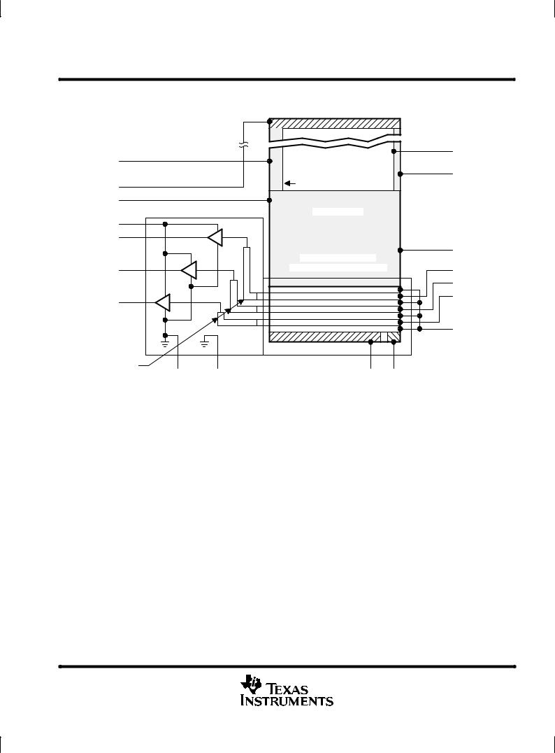
The TC241 consists of four basic functional blocks: (1) the image-sensing area, (2) the image-storage area,
(3) the multiplexer with serial registers and transfer gates, and (4) the buffer amplifier with charge-detection nodes. The location of each of these blocks is shown in the functional block diagram.
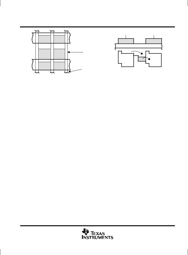
image-sensing storage areas
Cross sections with potential-well diagrams and top views of image-sensing and storage-area elements are shown in Figure 1 and Figure 2. As light enters the silicon in the image-sensing area, free electrons are generated and collected in the potential wells of the sensing elements. During this time, the antiblooming gate is activated by the application of a burst of pulses every horizontal-blanking interval. This prevents blooming caused by the spilling of charge from overexposed elements into neighboring elements. After the completion of integration, the signal charge is transferred into the storage area. To generate the dark reference necessary in subsequent video-processing circuits for restoration of the video-black level, 23 full columns and one half-column of elements at the left edge of the image-sensing area are shielded from incident light. Two full columns and one half-column of elements at the right of the image-sensing area are also shielded from incident light. The total number of elements per row is 780 (753 active elements plus 25 shielded elements and 2 transitional elements).
multiplexer with transfer gates and serial registers
The multiplexer and transfer-gates transfer charge line by line from the image-element columns into the corresponding serial register and prepare it for readout. Multiplexing is activated during the horizontal-blanking interval by applying appropriate pulses to the transfer gates and serial registers. The required pulse timing is shown in Figure 3. A drain is included in this area to provide the capability to quickly clear the image-sensing and storage areas of unwanted charge. Such charge can accumulate in the imager during the start-up of operation or under special circumstances when nonstandard TV operation is desired.
buffer amplifier with charge-detection nodes
The buffer amplifier converts charge into a video signal. Figure 4 shows the circuit diagram of a charge-detection node and one of the three amplifiers. As charge is transferred into the detection node, the potential of this node changes in proportion to the amount of signal received. This change is sensed by an MOS transistor and, after proper buffering, the signal is supplied to the output terminal of the image sensor. After the potential change has been sensed, the node is reset to a reference voltage supplied by an on-chip reference generator. The reset is accomplished by a reset gate that is connected internally to the serial register. The detection nodes and corresponding amplifiers are located some distance from the edge of the storage area; six dummy elements are used to span this distance. The location of the dummy elements is shown in the functional block diagram.
11.5 μm |
Clocked Barrier |
|
Light |
|
|
IAG |
ABG |
27 μm |
Virtual Barrier |
Antiblooming |
|
Antiblooming Gate |
Clocking Levels |
|
|
|
|
||
|
|
|
|
|
Virtual Well |
|
|
|
Clocked Well |
Accumulated Charge |
|
|
|
|
Figure 1. Charge-Accumulation Process
4 |
POST OFFICE BOX 655303 •DALLAS, TEXAS 75265 |
TC241 780- ×488-PIXEL CCD IMAGE SENSOR
SOCS006C ± AUGUST 1986 ± REVISED DECEMBER 1991
SAG
 Clocked Phase
Virtual Phase
Channel Stops
Figure 2. Charge-Transfer Process
POST OFFICE BOX 655303 •DALLAS, TEXAS 75265 |
5 |

TC241
780- ×488-PIXEL CCD IMAGE SENSOR
SOCS006C ± AUGUST 1986 ± REVISED DECEMBER 1991
Composite
Blanking
ABG
IAG
SAG
TRG
SRG 1
SRG2
SRG3
Expanded
Horizontal
Blanking Interval
Figure 3. Timing Diagram
6 |
POST OFFICE BOX 655303 •DALLAS, TEXAS 75265 |
 Loading...