


 Loading...
Texas Instruments SN74LVC1G17DBVR, SN74LVC1G17DCKR, SN74LVC1G17DRLR, SN74LVC1G17DRY2, SN74LVC1G17DSF2 Schematic [ru]
...PRODUCT |
SAMPLE & |
TECHNICAL |
TOOLS & |
SUPPORT & |
FOLDER |
BUY |
DOCUMENTS |
SOFTWARE |
COMMUNITY |
SN74LVC1G17
SCES351V –JULY 2001–REVISED APRIL 2014
SN74LVC1G17 Single Schmitt-Trigger Buffer
1 Features
•Available in Ultra Small 0.64-mm2 Package (DPW) With 0.5-mm Pitch
•Supports 5-V VCC Operation
•Inputs Accept Voltages to 5.5 V
•Max tpd of 4.6 ns at 3.3 V
•Low Power Consumption, 10-μA Max ICC
•±24-mA Output Drive at 3.3 V
•Ioff Supports Live Insertion, Partial-Power-Down Mode, and Back-Drive Protection
•Latch-Up Performance Exceeds 100 mA Per JESD 78, Class II
•ESD Protection Exceeds JESD 22
–2000-V Human-Body Model (A114-A)
–200-V Machine Model (A115-A)
–1000-V Charged-Device Model (C101)
2 Applications
•AV Receiver
•Audio Dock: Portable
•Blu-ray Player and Home Theater
•MP3 Player/Recorder
•Personal Digital Assistant (PDA)
•Power: Telecom/Server AC/DC Supply: Single Controller: Analog and Digital
•Solid State Drive (SSD): Client and Enterprise
•TV: LCD/Digital and High-Definition (HDTV)
•Tablet: Enterprise
•Video Analytics: Server
•Wireless Headset, Keyboard, and Mouse
3 Description
This single Schmitt-trigger buffer is designed for 1.65-V to 5.5-V VCC operation.
The SN74LVC1G17 device contains one buffer and performs the Boolean function Y = A.
The CMOS device has high output drive while maintaining low static power dissipation over a broad Vcc operating range.
The SN74LVC1G17 is available in a variety of packages, including the ultra-small DPW package with a body size of 0.8 mm × 0.8mm.
Device Information(1)
DEVICE NAME |
PACKAGE |
BODY SIZE |
|
SOT-23 (5) |
2.9mm × 1.6mm |
|
SC70 (5) |
2.0mm × 1.25mm |
SN74LVC1G17 |
X2SON (4) |
0.8mm × 0.8mm |
|
SON (6) |
1.45mm × 1.0mm |
|
SON (6) |
1.0mm × 1.0mm |
(1)For all available packages, see the orderable addendum at the end of the datasheet.
4 Simplified Schematic
An IMPORTANT NOTICE at the end of this data sheet addresses availability, warranty, changes, use in safety-critical applications, intellectual property matters and other important disclaimers. PRODUCTION DATA.

SN74LVC1G17
SCES351V –JULY 2001–REVISED APRIL 2014 |
www.ti.com |
Table of Contents
1 |
Features .................................................................. |
1 |
|
2 |
Applications ........................................................... |
1 |
|
3 |
Description ............................................................. |
1 |
|
4 |
Simplified Schematic............................................. |
1 |
|
5 |
Revision History..................................................... |
2 |
|
6 |
Pin Configuration and Functions ......................... |
3 |
|
7 |
Specifications......................................................... |
4 |
|
|
7.1 |
Absolute Maximum Ratings ..................................... |
4 |
|
7.2 |
Handling Ratings....................................................... |
4 |
|
7.3 |
Recommended Operating Conditions ...................... |
5 |
|
7.4 |
Thermal Information .................................................. |
5 |
|
7.5 |
Electrical Characteristics—DC Limit Changes.......... |
6 |
|
7.6 |
Switching Characteristics, CL = 15 pF ...................... |
7 |
7.7Switching Characteristics AC Limit, –40°C TO 85°C 7
7.8Switching Characteristics AC Limit, –40°C TO
|
125°C ......................................................................... |
7 |
7.9 |
Operating Characteristics.......................................... |
7 |
7.10 |
Typical Characteristics ............................................ |
7 |
8 Parameter Measurement Information .................. |
8 |
|
9 |
Detailed Description ............................................ |
10 |
|
|
9.1 |
Overview ................................................................. |
10 |
|
9.2 |
Functional Block Diagram ....................................... |
10 |
|
9.3 |
Feature Description................................................. |
10 |
|
9.4 |
Device Functional Modes........................................ |
10 |
10 |
Applications and Implementation...................... |
11 |
|
|
10.1 |
Application Information.......................................... |
11 |
|
10.2 |
Typical Application ............................................... |
11 |
11 |
Power Supply Recommendations ..................... |
12 |
|
12 |
Layout................................................................... |
12 |
|
|
12.1 |
Layout Guidelines ................................................. |
12 |
|
12.2 |
Layout Example .................................................... |
12 |
13 |
Device and Documentation Support ................. |
13 |
|
|
13.1 |
Trademarks ........................................................... |
13 |
|
13.2 |
Electrostatic Discharge Caution............................ |
13 |
|
13.3 |
Glossary ................................................................ |
13 |
14 |
Mechanical, Packaging, and Orderable |
|
|
|
Information ........................................................... |
13 |
|
5 |
Revision History |
|
Changes from Revision U (February 2014) to Revision V |
Page |
|
• Added Pin Functions table. .................................................................................................................................................... |
3 |
|
• Added Handling Ratings table. .............................................................................................................................................. |
4 |
|
• Added Thermal Information table. ......................................................................................................................................... |
5 |
|
• |
Added Typical Characteristics. .............................................................................................................................................. |
7 |
• Added Detailed Description section. .................................................................................................................................... |
10 |
|
•Added Application and Implementation section. ................................................................................................................. 11
•Added Power Supply Recommendations section. .............................................................................................................. 12
• |
Added Layout section. ......................................................................................................................................................... |
12 |
Changes from Revision T (November 2012) to Revision U |
Page |
|
• |
Added Applications................................................................................................................................................................. |
1 |
• Moved Tstg to Handling Ratings table. .................................................................................................................................... |
4 |
|
• Changed MAX operating free-air temperature from 85°C to 125°C....................................................................................... |
5 |
|
• Added –40°C to 125°C to Electrical Characteristics table...................................................................................................... |
6 |
|
• Added Switching Characteristics table for –40°C to 125°C temperature range..................................................................... |
7 |
|
Changes from Revision S (June 2011) to Revision T |
Page |
|
• Removed Ordering Information table. .................................................................................................................................... |
3 |
|
2 |
Submit Documentation Feedback |
Copyright © 2001–2014, Texas Instruments Incorporated |
Product Folder Links: SN74LVC1G17

|
|
|
|
|
|
|
|
|
|
|
|
|
|
|
|
|
|
|
|
|
|
|
|
SN74LVC1G17 |
||
www.ti.com |
|
|
|
|
|
|
|
|
|
|
|
|
|
|
|
|
|
|
|
SCES351V –JULY 2001–REVISED APRIL 2014 |
||||||
6 Pin Configuration and Functions |
|
|
|
|
|
|
|
|
|
|
|
|
|
|
|
|
||||||||||
|
|
DBV PACKAGE |
|
|
DCK PACKAGE |
|
DRL PACKAGE |
DRY PACKAGE |
||||||||||||||||||
|
|
|
(TOP VIEW) |
|
|
|
(TOP VIEW) |
|
|
(TOP VIEW) |
|
|
(TOP VIEW) |
|
||||||||||||
|
|
|
|
|
|
|
|
|
|
|
|
|
|
|
N.C. |
|
|
|
|
VCC |
|
|
|
|
|
|
|
|
|
|
|
|
|
N.C. |
|
|
1 |
5 |
|
|
VCC |
|
1 |
5 |
|
N.C. |
|
1 |
6 |
|
VCC |
||
|
|
|
|
|
|
|
|
|
|
|
|
|
|
|
|
|
|
|
|
|
|
|||||
N.C. |
|
|
1 |
5 |
|
|
VCC |
|
|
|
|
|
|
|
|
|
|
|
|
|
|
|
|
|
||
|
|
|
|
|
|
|
A |
|
|
2 |
|
|
|
|
A |
|
2 |
|
|
|
A |
|
2 |
5 |
|
N.C. |
|
|
|
|
|
|
|
|
|
|
|
|
|
|
|
|
|
|
|||||||||
|
|
|
|
|
|
|
|
|
|
|
|
|
|
|
|
|
|
|
|
|
|
|
|
|
||
A |
|
|
2 |
|
|
|
GND |
|
|
3 |
4 |
|
|
Y |
GND |
|
3 |
4 |
|
Y |
GND |
|
3 |
4 |
|
Y |
|
|
|
|
|
|
|
|
|
|
|
|
|
||||||||||||||
|
|
|
|
|
|
|
|
|
|
|
|
|
|
|
|
|
|
|
|
|||||||
GND |
|
|
|
|
|
|
|
|
|
|
|
|
|
|
|
|
|
|
|
|
|
|
||||
|
|
|
|
|
|
|
|
|
|
|
|
|
|
|
|
|
||||||||||
|
|
3 |
4 |
|
|
Y |
|
|
|
|
|
|
|
|
|
|
|
|
|
|
|
|
|
|
|
|
|
|
|
|
|
|
|
|
|
|
|
|
|
|
|
|
|
|
|
|
|
|
|
||||
|
|
|
|
|
|
|
|
|
|
|
|
|
|
|
|
|
|
|
|
|
|
|
||||
|
|
|
|
|
|
|
|
|
|
|
YZP PACKAGE |
|
|
YZV PACKAGE |
DSF PACKAGE |
|||||||||||
|
|
|
|
|
|
|
|
|
|
|
|
|
||||||||||||||
|
|
|
|
|
|
|
|
|
|
|
|
|||||||||||||||
|
|
|
|
|
|
DPW PACKAGE |
|
|
|
(TOP VIEW) |
|
|
(TOP VIEW) |
|
(TOP VIEW) |
|
||||||||||
|
|
|
|
|
|
|
|
|
|
|
|
|
|
|
|
|
|
|
|
|
|
|
|
|
||
|
(TOP VIEW) |
||
|
N.C. 1 |
5 |
V |
GND |
|
3 |
CC |
|
|
||
|
A 2 |
4 |
Y |
DNU
A
GND
A1 |
A2 |
VCC |
A |
B1 |
B2 |
|
GND |
C1 |
C2 |
Y |
|
|
|
VCC |
N.C. |
A1 |
A2 |
|
|
|
|
A |
|
B1 |
B2 |
Y |
GND |
1 6 VCC
2 5 N.C.
3 4 Y
N.C. – NO INTERNAL CONNECTION
SEE MECHANICAL DRAWINGS FOR DIMENSIONS.
DNU – DO NOT USE
|
|
|
|
|
Pin Functions |
|
|
|
PIN |
|
|
|
|
NAME |
DBV, DCK, |
DRY, DSF |
YZP |
YZV |
|
DESCRIPTION |
DRL, DPW |
|
|
||||
|
|
|
|
|
|
|
NC |
1 |
1, 5 |
A1, B2 |
– |
|
Not connected |
A |
2 |
2 |
B1 |
A1 |
|
Input |
|
|
|
|
|
|
|
GND |
3 |
3 |
C1 |
B1 |
|
Ground |
|
|
|
|
|
|
|
Y |
4 |
4 |
C2 |
B2 |
|
Output |
VCC |
5 |
6 |
A2 |
A2 |
|
Power terminal |
Copyright © 2001–2014, Texas Instruments Incorporated |
Submit Documentation Feedback |
3 |
Product Folder Links: SN74LVC1G17

SN74LVC1G17
SCES351V –JULY 2001–REVISED APRIL 2014 |
www.ti.com |
7 Specifications
7.1 Absolute Maximum Ratings(1)
over operating free-air temperature range (unless otherwise noted)
|
|
|
MIN |
MAX |
UNIT |
VCC |
Supply voltage range |
|
–0.5 |
6.5 |
V |
V |
Input voltage range(2) |
|
–0.5 |
6.5 |
V |
I |
|
|
|
|
|
V |
Voltage range applied to any output in the high-impedance or power-off state(2) |
–0.5 |
6.5 |
V |
|
O |
|
|
|
|
|
V |
Voltage range applied to any output in the high or low state(2)(3) |
–0.5 |
V + 0.5 |
V |
|
O |
|
|
|
CC |
|
IIK |
Input clamp current |
VI < 0 |
|
–50 |
mA |
IOK |
Output clamp current |
VO < 0 |
|
–50 |
mA |
IO |
Continuous output current |
|
|
±50 |
mA |
|
Continuous current through VCC or GND |
|
|
±100 |
mA |
(1)Stresses beyond those listed under Absolute Maximum Ratings may cause permanent damage to the device. These are stress ratings only, and functional operation of the device at these or any other conditions beyond those indicated under Recommended Operating Conditions tables is not implied. Exposure to absolute-maximum-rated conditions for extended periods may affect device reliability.
(2)The input and output negative-voltage ratings may be exceeded if the input and output current ratings are observed.
(3)The value of VCC is provided in the Recommended Operating Conditions table.
7.2 |
Handling Ratings |
|
|
|
||
|
|
|
MIN |
MAX |
|
UNIT |
Tstg |
|
Storage temperature range |
|
–65 |
150 |
°C |
VESD |
(1) |
Human-Body Model (HBM)(2) |
|
0 |
2 |
kV |
|
Charged-Device Model (CDM)(3) |
|
0 |
1 |
kV |
|
|
|
|
||||
(1)Electrostatic discharge (ESD) to measure device sensitivity and immunity to damage caused by assembly line electrostatic discharges in to the device.
(2)Level listed above is the passing level per ANSI, ESDA, and JEDEC JS-001. JEDEC document JEP155 states that 500-V HBM allows safe manufacturing with a standard ESD control process.
(3)Level listed above is the passing level per EIA-JEDEC JESD22-C101. JEDEC document JEP157 states that 250-V CDM allows safe manufacturing with a standard ESD control process.
4 |
Submit Documentation Feedback |
Copyright © 2001–2014, Texas Instruments Incorporated |
Product Folder Links: SN74LVC1G17

SN74LVC1G17
www.ti.com SCES351V –JULY 2001–REVISED APRIL 2014
7.3 Recommended Operating Conditions(1)
|
|
|
MIN |
MAX |
UNIT |
VCC |
Supply voltage |
Operating |
1.65 |
5.5 |
V |
Data retention only |
1.5 |
|
|||
|
|
|
|
||
VI |
Input voltage |
0 |
5.5 |
V |
|
VO |
Output voltage |
0 |
VCC |
V |
|
|
|
VCC = 1.65 V |
|
–4 |
|
|
|
VCC = 2.3 V |
|
–8 |
|
IOH |
High-level output current |
VCC = 3 V |
|
–16 |
mA |
|
|
|
–24 |
|
|
|
|
|
|
|
|
|
|
VCC = 4.5 V |
|
–32 |
|
|
|
VCC = 1.65 V |
|
4 |
|
|
|
VCC = 2.3 V |
|
8 |
|
IOL |
Low-level output current |
VCC = 3 V |
|
16 |
mA |
|
|
|
24 |
|
|
|
|
|
|
|
|
|
|
VCC = 4.5 V |
|
32 |
|
TA |
Operating free-air temperature |
–40 |
125 |
°C |
|
(1)All unused inputs of the device must be held at VCC or GND to ensure proper device operation. Refer to the TI application report,
Implications of Slow or Floating CMOS Inputs, literature number SCBA004.
7.4 Thermal Information
|
|
|
|
|
SN74LVC1G17 |
|
|
|
|
||
|
THERMAL METRIC(1) |
DBV |
DCK |
DRL |
|
DRY |
|
YZP |
DPW |
YZV |
UNIT |
|
|
5 PINS |
5 PINS |
5 PINS |
|
6 PINS |
|
5 PINS |
4 PINS |
4 PINS |
|
RθJA |
Junction-to-ambient thermal resistance |
229 |
280 |
350 |
|
608 |
|
130 |
340 |
181 |
|
RθJC(top) |
Junction-to-case (top) thermal resistance |
164 |
66 |
121 |
|
432 |
|
54 |
215 |
1 |
|
RθJB |
Junction-to-board thermal resistance |
62 |
67 |
171 |
|
446 |
|
51 |
294 |
39 |
°C/W |
ψJT |
Junction-to-top characterization parameter |
44 |
2 |
11 |
|
191 |
|
1 |
41 |
8 |
|
|
|
|
|||||||||
ψJB |
Junction-to-board characterization parameter |
62 |
66 |
169 |
|
442 |
|
50 |
294 |
38 |
|
RθJC(bot) |
Junction-to-case (bottom) thermal resistance |
– |
– |
– |
|
198 |
|
– |
250 |
– |
|
(1)For more information about traditional and new thermal metrics, see the IC Package Thermal Metrics application report, SPRA953.
Copyright © 2001–2014, Texas Instruments Incorporated |
Submit Documentation Feedback |
5 |
Product Folder Links: SN74LVC1G17

SN74LVC1G17
SCES351V –JULY 2001–REVISED APRIL 2014 |
www.ti.com |
7.5 Electrical Characteristics—DC Limit Changes
over recommended operating free-air temperature range (unless otherwise noted)
PARAMETER |
TEST CONDITIONS |
VCC |
|
25°C |
|
–40°C TO 85°C |
|
–40°C TO 125°C |
|
UNIT |
|||||
MIN |
TYP(1) |
MAX |
MIN TYP(1) |
MAX |
MIN |
TYP |
MAX |
||||||||
|
|
|
|
|
|
|
|||||||||
|
|
|
|
|
1.65 V |
|
|
|
0.76 |
1.13 |
0.76 |
|
1.13 |
|
|
VT+ |
|
|
|
2.3 V |
|
|
|
1.08 |
1.56 |
1.08 |
|
1.56 |
|
||
(Positive-going |
|
|
|
|
|
|
|
|
|
|
|
|
|||
|
|
3 V |
|
|
|
1.48 |
1.92 |
1.48 |
|
1.92 |
V |
||||
input threshold |
|
|
|
|
|
|
|||||||||
|
|
|
|
|
|
|
|
|
|
|
|
||||
voltage) |
|
|
|
4.5 V |
|
|
|
2.19 |
2.74 |
2.19 |
|
2.74 |
|
||
|
|
|
|
|
5.5 V |
|
|
|
2.65 |
3.33 |
2.65 |
|
3.33 |
|
|
|
|
|
|
|
1.65 V |
|
|
|
0.35 |
0.59 |
0.35 |
|
0.59 |
|
|
|
|
|
|
|
|
|
|
|
|
|
|
|
|
||
VT– |
|
|
|
2.3 V |
|
|
|
0.56 |
0.88 |
0.56 |
|
0.88 |
|
||
(Negative-going |
|
|
|
|
|
|
|
|
|
|
|
|
|||
|
|
3 V |
|
|
|
0.89 |
1.2 |
0.89 |
|
1.2 |
V |
||||
input threshold |
|
|
|
|
|
|
|||||||||
voltage) |
|
|
|
4.5 V |
|
|
|
1.51 |
1.97 |
1.51 |
|
1.97 |
|
||
|
|
|
|
|
5.5 V |
|
|
|
1.88 |
2.4 |
1.88 |
|
2.4 |
|
|
|
|
|
|
|
|
|
|
|
|
|
|
|
|
|
|
|
|
|
|
|
1.65 V |
|
|
|
0.36 |
0.64 |
0.36 |
|
0.64 |
|
|
VT |
|
|
|
2.3 V |
|
|
|
0.45 |
0.78 |
0.45 |
|
0.78 |
|
||
Hysteresis |
|
|
3 V |
|
|
|
0.51 |
0.83 |
0.51 |
|
0.83 |
V |
|||
(VT+ – VT–) |
|
|
|
|
|
|
|
|
|
|
|
|
|||
|
|
4.5 V |
|
|
|
0.58 |
0.93 |
0.58 |
|
0.93 |
|
||||
|
|
|
|
|
|
|
|
|
|
||||||
|
|
|
|
|
|
|
|
|
|
|
|
|
|
|
|
|
|
|
|
|
5.5 V |
|
|
|
0.69 |
1.04 |
0.69 |
|
1.04 |
|
|
|
|
|
IOH = –100 μA |
1.65 V to |
|
|
|
VCC – 0.1 |
|
VCC – 0.1 |
|
|
|
||
|
|
|
5.5 V |
|
|
|
|
|
|
|
|||||
|
|
|
|
|
|
|
|
|
|
|
|
|
|
||
|
|
|
IOH = –4 mA |
1.65 V |
|
|
|
1.2 |
|
1.2 |
|
|
|
||
VOH |
|
IOH = –8 mA |
2.3 V |
|
|
|
1.9 |
|
1.9 |
|
|
V |
|||
|
|
|
IOH = –16 mA |
3 V |
|
|
|
2.4 |
|
2.4 |
|
|
|
||
|
|
|
IOH = –24 mA |
|
|
|
2.3 |
|
2.3 |
|
|
|
|||
|
|
|
|
|
|
|
|
|
|
|
|||||
|
|
|
IOH = –32 mA |
4.5 V |
|
|
|
3.8 |
|
3.8 |
|
|
|
||
|
|
|
IOL = 100 μA |
1.65 V to |
|
|
|
|
0.1 |
|
|
0.1 |
|
||
|
|
|
5.5 V |
|
|
|
|
|
|
|
|||||
|
|
|
|
|
|
|
|
|
|
|
|
|
|
||
|
|
|
IOL = 4 mA |
1.65 V |
|
|
|
|
0.45 |
|
|
0.45 |
|
||
VOL |
|
IOL = 8 mA |
2.3 V |
|
|
|
|
0.3 |
|
|
0.3 |
V |
|||
|
|
|
IOL = 16 mA |
3 V |
|
|
|
|
0.4 |
|
|
0.4 |
|
||
|
|
|
IOL = 24 mA |
|
|
|
|
0.55 |
|
|
0.55 |
|
|||
|
|
|
|
|
|
|
|
|
|
|
|||||
|
|
|
IOL = 32 mA |
4.5 V |
|
|
|
|
0.55 |
|
|
0.55 |
|
||
II |
|
A input |
VI = 5.5 V or GND |
0 to |
|
|
|
|
±5 |
|
|
±5 |
μA |
||
|
5.5 V |
|
|
|
|
|
|
||||||||
|
|
|
|
|
|
|
|
|
|
|
|
|
|
||
Ioff |
|
VI or VO = 5.5 V |
0 |
|
|
|
|
±10 |
|
|
±10 |
μA |
|||
|
|
|
VI = 5.5 V or GND, |
|
1.65 V to |
|
|
|
|
10 |
|
|
10 |
|
|
|
|
|
|
5.5 V |
|
|
|
|
|
|
|
||||
ICC |
|
|
IO = 0 |
|
|
|
|
|
|
|
|
μA |
|||
|
VI = 3.6 V or GND, |
3 V to |
|
0.5 |
1.5 |
|
|
|
|
|
|||||
|
|
|
|
3.6 V |
|
|
|
|
|
|
|
||||
|
|
|
|
|
|
|
|
|
|
|
|
|
|
||
|
|
|
|
|
|
|
|
|
|
|
|
|
|
|
|
ICC |
|
One input at VCC – 0.6 V, |
3 V to |
|
|
|
|
500 |
|
|
500 |
μA |
|||
|
Other inputs at VCC or GND |
5.5 V |
|
|
|
|
|
|
|||||||
|
|
|
|
|
|
|
|
|
|
|
|
||||
CI |
|
VI = VCC or GND |
3.3 V |
|
4.5 |
|
|
|
|
|
|
pF |
|||
(1)All typical values are at VCC = 3.3 V, TA = 25°C.
6 |
Submit Documentation Feedback |
Copyright © 2001–2014, Texas Instruments Incorporated |
Product Folder Links: SN74LVC1G17

SN74LVC1G17
www.ti.com |
SCES351V –JULY 2001–REVISED APRIL 2014 |
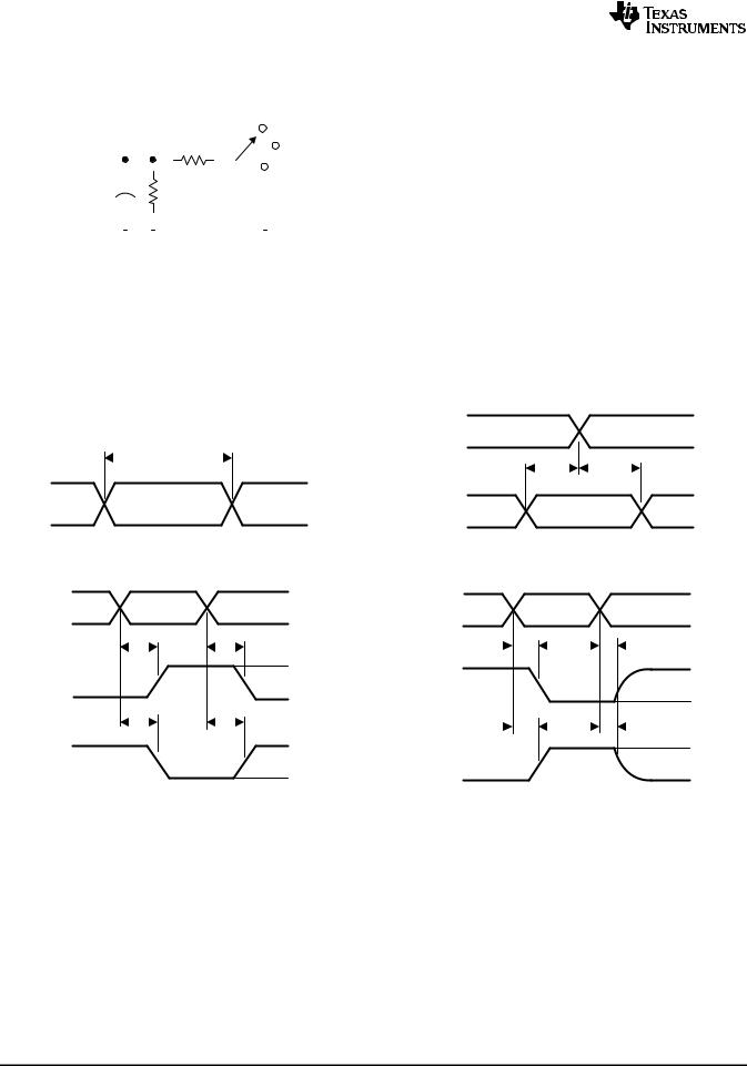
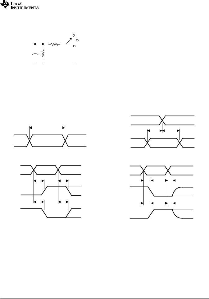
7.6 Switching Characteristics, CL = 15 pF
over recommended operating free-air temperature range, CL = 15 pF (unless otherwise noted) (see Figure 3 )
|
|
|
|
|
|
–40°C TO 85°C |
|
|
|
|
|
||
PARAMETER |
FROM |
TO |
VCC = |
1.8 V |
VCC = 2.5 V |
VCC = 3.3 V |
VCC |
= 5 V |
UNIT |
||||
(INPUT) |
(OUTPUT) |
± 0.15 V |
± 0.2 V |
± 0.3 V |
± 0.5 V |
||||||||
|
|
||||||||||||
|
|
|
MIN |
MAX |
MIN |
MAX |
MIN |
MAX |
MIN |
|
MAX |
|
|
tpd |
A |
Y |
2.8 |
9.9 |
1.6 |
5.5 |
1.5 |
4.6 |
0.9 |
4.4 |
ns |
||
7.7 Switching Characteristics AC Limit, –40°C TO 85°C
over recommended operating free-air temperature range, CL = 30 pF or 50 pF (unless otherwise noted) (see Figure 4)
|
|
|
|
|
|
–40°C TO 85°C |
|
|
|
|
|
||
PARAMETER |
FROM |
TO |
VCC = |
1.8 V |
VCC = 2.5 V |
VCC = 3.3 V |
VCC |
= 5 V |
UNIT |
||||
(INPUT) |
(OUTPUT) |
± 0.15 V |
± 0.2 V |
± 0.3 V |
± 0.5 V |
||||||||
|
|
||||||||||||
|
|
|
MIN |
MAX |
MIN |
MAX |
MIN |
MAX |
MIN |
|
MAX |
|
|
tpd |
A |
Y |
3.8 |
11 |
2 |
6.5 |
1.8 |
5.5 |
1.2 |
5 |
ns |
||
7.8 Switching Characteristics AC Limit, –40°C TO 125°C
over recommended operating free-air temperature range, CL = 30 pF or 50 pF (unless otherwise noted) (see Figure 4)
|
|
|
|
|
|
–40°C TO 125°C |
|
|
|
|
|
||
PARAMETER |
FROM |
TO |
VCC = |
1.8 V |
VCC = 2.5 V |
VCC = 3.3 V |
VCC |
= 5 V |
UNIT |
||||
(INPUT) |
(OUTPUT) |
± 0.15 V |
± 0.2 V |
± 0.3 V |
± 0.5 V |
||||||||
|
|
||||||||||||
|
|
|
MIN |
MAX |
MIN |
MAX |
MIN |
MAX |
MIN |
|
MAX |
|
|
tpd |
A |
Y |
3.8 |
13 |
2 |
8 |
1.8 |
6.5 |
1.2 |
6 |
ns |
||
7.9 |
Operating Characteristics |
|
|
|
|
|
|
TA = 25°C |
|
|
|
|
|
|
|
|
PARAMETER |
TEST |
VCC = 1.8 V |
VCC = 2.5 V |
VCC = 3.3 V |
VCC = 5 V |
UNIT |
|
CONDITIONS |
TYP |
TYP |
TYP |
TYP |
||
|
|
|
|||||
Cpd |
Power dissipation capacitance |
f = 10 MHz |
20 |
21 |
22 |
26 |
pF |
7.10 Typical Characteristics
TPD - ns
3.8 |
TPD |
3.7 |
3.6
3.5
3.4
3.3
3.2
3.1 -100 -50 0 50 100 150
Temperature - °C
D001
Figure 1. Across Temperature at 3.3V Vcc
TPD - ns
8
TPD
7
6
5
4
3
2
1
0
0 1 2 3 4 5 6
Vcc - V
D002
Figure 2. Across Vcc at 25°C
Copyright © 2001–2014, Texas Instruments Incorporated |
Submit Documentation Feedback |
7 |
Product Folder Links: SN74LVC1G17
SN74LVC1G17
SCES351V –JULY 2001–REVISED APRIL 2014 |
|
|
|
|
|
|
|
|
|
www.ti.com |
|||||||||||||||
8 Parameter Measurement Information |
|
|
|
||||||||||||||||||||||
|
|
|
|
|
|
|
|
|
|
|
|
|
|
|
|
|
|
|
|
|
VLOAD |
|
|
|
|
|
|
|
|
|
|
|
|
|
|
|
|
|
|
RL |
S1 |
|
|
OPEN |
|
|
|
||||
FROM OUTPUT |
|
|
|
|
|
|
|
|
|
|
|
|
|
|
|
|
|
TEST |
S1 |
|
|||||
|
|
|
|
|
|
|
|
|
|
|
|
|
|
|
|
|
|
|
|
||||||
UNDER TEST |
|
|
|
|
|
|
|
|
|
|
|
|
|
|
|
|
|
|
GND |
TPLH/TPHL |
OPEN |
|
|||
CL |
|
|
|
|
|
|
|
|
|
|
|
|
|
|
|
|
|
|
|
|
|
|
|||
|
|
|
|
|
|
|
|
|
|
|
|
|
|
|
|
|
|
|
|
|
|||||
|
|
|
|
|
|
|
|
|
|
RL |
|
|
|
|
|
|
|
TPLZ/TPZL |
VLOAD |
|
|||||
(SEE NOTE A) |
|
|
|
|
|
|
|
|
|
|
|
|
|
|
|
|
|
|
|||||||
|
|
|
|
|
|
|
|
|
|
|
|
|
|
|
|
|
|
|
|
|
|
|
TPHZ/TPZH |
GND |
|
|
|
|
|
|
|
|
|
|
|
|
|
|
|
|
|
|
|
|
|
|
|
|
|
|
|
|
|
|
|
|
|
|
|
|
|
|
|
|
|
|
|
|
|
|
|
|
|
|
|
|
|
INPUT
INPUT
OUTPUT
OUTPUT
LOAD CIRCUIT
|
|
|
|
|
|
|
|
|
|
|
|
|
|
|
|
|
|
|
|
|
|
|
|
|
|
|
|
|
INPUTS |
|
|
|
|
|
|
|
|
|
|
|
|
|
|
|
|
|
|
|
|
|
|
|
|
|
|
|
|
|
|
|
|
|
|
|
|
|||
|
|
|
|
|
|
|
|
|
|
|
|
|
|
VCC |
|
|
|
|
|
|
|
|
|
|
|
|
|
|
VM |
|
VLOAD |
CL |
|
|
|
|
|
|
|
RL |
|
|
|
|
|
V |
|
|
||||||||||||||||||||
|
|
|
|
|
|
|
|
|
|
|
|
|
|
|
|
|
|
|
|
|
VI |
|
TR/TF |
|
|
|
|
|
|
|
|
|
|
|
|
|
|
|
|
|
|
|||||||||||||||||||||||||||
|
|
|
|
|
|
|
|
|
|
|
|
|
|
|
|
|
|
|
|
|
|
|
|
|
|
|
|
|
|
|
|
|
|
|
|
|
|
|
|
|||||||||||||||||||||||||||||
|
|
|
|
|
|
|
|
|
|
1.8 V ± 0.15 V |
|
|
|
|
|
VCC |
|
≤2 NS |
VCC/2 |
|
2 × VCC |
15 PF |
|
|
|
|
|
1 MΩ |
|
|
0.15 V |
|
|
|
|
|
|
|||||||||||||||||||||||||||||||
|
|
|
|
|
|
|
|
|
|
2.5 V ± 0.2 V |
|
|
|
|
|
VCC |
|
≤2 NS |
VCC/2 |
|
2 × VCC |
15 PF |
|
|
|
|
|
1 MΩ |
|
|
0.15 V |
|
|
|||||||||||||||||||||||||||||||||||
|
|
|
|
|
|
|
|
|
|
3.3 V ± 0.3 V |
|
|
|
|
|
3 V |
|
≤2.5 NS |
1.5 V |
|
6 V |
15 PF |
|
|
|
|
|
1 MΩ |
|
|
|
0.3 V |
|
|
||||||||||||||||||||||||||||||||||
|
|
|
|
|
|
|
|
|
|
5 V ± 0.5 V |
|
|
|
|
|
VCC |
|
≤2.5 NS |
VCC/2 |
|
2 × VCC |
15 PF |
|
|
|
|
|
1 MΩ |
|
|
|
0.3 V |
|
|
||||||||||||||||||||||||||||||||||
|
|
|
|
|
|
|
|
|
|
|
|
|
|
|
|
|
|
|
|
|
|
|
|
|
|
|
|
|
|
|
|
|
|
TIMING INPUT |
|
|
|
|
|
|
|
|
|
|
|
|
|
|
|
|
|
|
VM |
|||||||||||||||
|
|
|
|
|
|
|
|
|
|
|
|
|
|
|
|
|
|
|
|
|
|
|
|
|
|
|
|
|
|
|
|
|
|
|
|
|
|
|
|
|
|
|
|
|
|
|
|
|
|
|
|
|||||||||||||||||
|
|
|
|
|
|
|
|
|
|
|
|
|
|
|
|
|
|
|
|
|
|
|
|
|
|
|
|
|
|
|
|
|
|
|
|
|
|
|
|
|
|
|
|
|
|
|
|
|
|
|
||||||||||||||||||
|
|
|
|
|
|
|
|
|
|
|
|
|
TW |
|
|
|
|
|
|
|
|
|
|
|
|
|
|
|
|
|
|
|
|
|
|
|
|
|
|
|
|
|
|
|
|
|
|
|
|
|
|
|
|
|
|
|
|
|
|
|
|
|
|
|
|
|
|
|
|
|
|
|
|
|
|
|
|
|
|
|
|
|
|
|
|
|
|
|
|
|
|
|
|
|
|
|
|
|
|
|
|
|
|
|
|
|
|
|
|
|
|
|
|
|
|
|
|
|
|
|
|
|
|
|
|
|
|
|
|
|
|
|
|
|
|
||
|
|
|
|
|
|
|
|
|
|
|
|
|
|
|
|
|
|
|
|
|
|
|
|
|
|
|
|
|
|
|
|
|
|
|
|
|
|
|
|
|
|
|
|
|
|
|
|
|
|
|
|
|
|
|
|
|
|
|
|
|
|
|
|
|
|
|
|
|
|
|
|
|
|
|
|
|
|
|
|
|
|
|
|
|
|
|
|
|
|
|
|
|
|
|
|
|
|
|
|
|
VI |
|
|
|
|
|
|
|
|
|
|
|
|
|
TSU |
|
|
|
|
|
|
|
|
TH |
|||||||||||||
|
|
|
|
|
|
|
|
|
|
|
|
|
|
|
|
|
|
|
|
|
|
|
|
|
|
|
|
|
|
|
|
|
|
|
|
|
|
|
|
|
|
|
|
|
|
|
|
|
|
|
|
|
|
|||||||||||||||
|
|
|
|
VM |
|
|
|
|
|
|
|
|
VM |
0 V |
|
|
DATA INPUT |
|
|
|
|
|
|
|
|
|
VM |
|
|
|
|
|
|
|
|
|
|
|
|
|
|
|
|
|
VM |
|||||||||||||||||||||||
|
|
|
|
|
|
|
|
|
|
|
|
|
|
|
|
|
|
|
|
|
|
|
|
|
|
|
|
|
|
|
|
|
|
|
|
|
|
|
|
|||||||||||||||||||||||||||||
|
|
|
|
|
|
|
|
|
|
|
|
|
|
|
|
|
|
|
|
|
|
|
|
|
|
|
|
|
|
|
|
|
|
|
|
|
|
|
|
|||||||||||||||||||||||||||||
|
|
|
|
|
|
|
|
|
|
|
|
|
|
|
|
|
|
|
|
|
|
|
|
|
|
|
|
|
|
|
|
|
|
|
|
|
|
|
|
|
|
|
|
|
|
|
|
|
|
|
|
|
|
|
|
|
|
|
|
|||||||||
|
|
|
|
|
|
|
|
|
|
|
|
|
|
|
|
|
|
|
|
|
|
|
|
|
|
|
|
|
|
|
|
|
|
|
|
|
|
|
|
|
|
|
|
|
|
|
|
|
|
|
|
|
|
|
|
|
|
|
|
|
|
|
|
|
|
|
|
|
|
VOLTAGE WAVEFORMS |
|
|
|
|
|
|
|
|
VOLTAGE WAVEFORMS |
||||||||||||||||||||||||||||||||||||||||||||||||||||||||||
|
|
|
|
|
PULSE DURATION |
|
|
|
|
|
|
|
SETUP AND HOLD TIMES |
|||||||||||||||||||||||||||||||||||||||||||||||||||||||
|
|
|
|
|
|
|
|
|
|
|
|
|
|
|
|
|
|
|
|
|
|
|
|
|
|
|
|
|
|
|
|
VI |
|
|
OUTPUT |
|
|
|
|
|
|
|
|
|
|
|
|
|
|
|
|
|
|
|
|
|
|
|
|
|
|
|
|
|
|
|
|
|
|
|
|
|
|
|
|
|
|
|
VM |
|
|
|
VM |
|
|
|
|
|
|
|
|
|
VM |
|
|
|
|
|
|
|
|
VM |
|||||||||||||||||||||||||||||||||||
|
|
|
|
|
|
|
|
|
|
|
|
|
|
|
|
|
|
|
|
|
|
|
|
|
|
|
|
|
|
|
|
0 V |
|
|
CONTROL |
|
|
|
|
|
|
|
|
|
|
|
|
|
|
|
|
|
|
|
|
|
|
|
|
|
|
|
|
|
|
|
|
|
|
|
|
|
|
|
|
|
|
|
|
|
|
|
|
|
|
|
|
|
|
|
|
|
|
|
|
|
|
|
|
|
|
|
|
|
|
|
|
|
|
|
|
|
|
|
|
|
|
|
|
|
|
|
|
|
|
|
|
|
|
|
|
|
|
|
|
|
|
TPLH |
|
|
|
|
|
|
|
|
|
|
|
|
|
|
|
|
|
|
TPHL |
VOH |
|
|
OUTPUT |
TPZL |
|
|
|
|
|
|
|
|
|
|
|
|
|
|
|
|
|
|
|
|
|
|
|
|
|
|
|
|
|
|
TPLZ |
|||||||||||||
|
|
|
|
|
|
|
|
|
|
|
|
|
|
|
|
|
|
|
|
|
|
|
|
|
|
|
|
|
|
|
|
|
|
|
|
|
|
|
|
|
|
|
|
|
|
|||||||||||||||||||||||
|
|
|
|
|
|
|
|
|
|
|
|
|
|
|
|
|
|
|
|
|
|
|
|
|
|
|
|
|
|
|
|
|
|
|
|
|
|
|||||||||||||||||||||||||||||||
|
|
|
|
|
|
|
|
|
|
|
|
|
|
|
|
|
|
|
|
|
|
|
|
|
|
|
|
|
|
|
|
|
|
|
|
|
|
|
|
|
|
|
|
|
|
|
|
|
|
|
|
|
|
|
|
|
|
|
|
|
|
|
|
|
|
|
||
|
|
|
|
|
|
|
|
|
|
|
|
|
|
VM |
|
|
|
|
|
|
|
|
|
|
VM |
|
|
WAVEFORM 1 |
|
|
|
|
|
|
|
|
|
|
|
VM |
|
|
|
|
|
|
|
|
|
|
|
|
|
|
|
|
|
|
||||||||||
|
|
|
|
|
|
|
|
|
|
|
|
|
|
|
|
|
|
|
|
|
|
|
|
|
|
|
|
|
|
|
|
VOL |
|
|
S1 AT VLOAD |
|
|
|
|
|
|
|
|
|
|
|
|
|
|
|
|
|
|
|
|
|
|
|
|
|
VOL + V |
|||||||
|
|
|
|
|
|
|
|
|
|
|
|
|
|
|
|
|
|
|
|
|
|
|
|
|
|
|
|
|
|
|
|
|
(SEE NOTE B) |
|
|
|
|
|
|
|
|
|
|
|
|
|
|
|
|
|
|
|
|
|
|
|
|
|
|
|
|
|
|
|
|
|
||
|
|
|
|
|
|
|
|
|
|
|
|
|
|
|
|
|
|
|
|
|
|
|
|
|
|
|
|
|
|
|
|
|
|
|
|
|
|
|
|
|
|
|
|
|
|
|
|
|
|
|
|
|
|
|
|
|
|
|
|
|
|
|
|
|
|
|
||
TPHL |
|
|
|
|
|
|
|
|
|
|
|
|
|
|
|
|
|
|
TPLH |
|
|
|
|
|
|
|
|
|
|
|
|
|
|
|
|
|
|
|
|
|
|
|
|
|
|
|
|
|
|
|
|
|
|
|
|
|
||||||||||||
|
|
|
|
|
|
|
|
|
|
|
|
|
|
|
|
|
|
|
|
|
|
|
|
|
|
|
|
|
|
|
|
|
|
|
|
|
|
|
|
|
|
|
|
|
|
|
|
|
|
|||||||||||||||||||
|
|
|
|
|
|
|
|
|
|
|
|
|
|
|
|
|
|
|
|
|
|
|
|
|
|
|
|
|
|
|
TPZH |
|
|
|
|
|
|
|
|
|
|
|
|
|
|
|
|
|
|
|
|
|
|
|
|
|
|
|
|
|
TPHZ |
|||||||
|
|
|
|
|
|
|
|
|
|
|
|
|
|
|
|
|
|
|
|
|
|
|
|
|
|
|
|
|
|
|
|
|
|
|
|
|
|
|
|
|
|
|
|
|
|
|
|
|
|
|
|
|
|
|
|
|
|
|
|
|
|
|
|
|
||||
|
|
|
|
|
|
|
|
|
|
|
|
|
|
|
|
|
|
|
|
|
|
|
|
|
|
|
|
|
|
|
|
VOH |
|
|
OUTPUT |
|
|
|
|
|
|
|
|
|
|
|
|
|
|
|
|
|
|
|
|
|
|
|
|
|
VOH – V |
|||||||
|
|
|
|
|
|
|
|
|
|
|
|
|
|
|
|
|
|
|
|
|
|
|
|
|
|
|
|
|
|
|
|
|
|
|
|
|
|
|
|
|
|
|
|
|
|
|
|
|
|
|
|
|
|
|
|
|
|
|||||||||||
|
|
|
|
|
|
|
|
|
|
|
|
|
|
VM |
|
|
|
|
|
|
|
|
|
|
VM |
|
|
WAVEFORM 2 |
|
|
|
|
|
|
|
|
|
|
|
VM |
|
|
|
|
|
|
|
|
|
|
|
|
|
|
|
|
|
|
||||||||||
|
|
|
|
|
|
|
|
|
|
|
|
|
|
|
|
|
|
|
|
|
|
|
|
|
|
|
|
|
|
|
|
VOL |
|
|
S1 AT GND |
|
|
|
|
|
|
|
|
|
|
|
|
|
|
|
|
|
|
|
|
|
|
|
|
|
|
|
|
|
||||
|
|
|
|
|
|
|
|
|
|
|
|
|
|
|
|
|
|
|
|
|
|
|
|
|
|
|
|
|
|
|
|
|
|
|
|
|
|
|
|
|
|
|
|
|
|
|
|
|
|
|
|
|
|
|
|
|
|
|
|
|
|
|
|
|
|
|
||
|
|
|
|
|
|
|
|
|
|
|
|
|
|
|
|
|
|
|
|
|
|
|
|
|
|
|
|
|
|
|
|
|
(SEE NOTE B) |
|
|
|
|
|
|
|
|
|
|
|
|
|
|
|
|
|
|
|
|
|
|
|
|
|
|
|
|
|
|
|
|
|
||
|
|
|
|
|
|
|
|
|
VOLTAGE WAVEFORMS |
|
|
|
|
|
|
VOLTAGE WAVEFORMS |
||||||||||||||||||||||||||||||||||||||||||||||||||||
|
|
|
|
|
|
|
|
|
|
|
|
|
|
|
|
|
||||||||||||||||||||||||||||||||||||||||||||||||||||
|
|
|
|
PROPAGATION DELAY TIMES |
|
|
|
|
|
ENABLE AND DISABLE TIMES |
||||||||||||||||||||||||||||||||||||||||||||||||||||||||||
INVERTING AND NONINVERTING OUTPUTS |
|
|
|
LOWAND HIGH-LEVEL ENABLING |
||||||||||||||||||||||||||||||||||||||||||||||||||||||||||||||||
VI
0 V
VI
0 V
VI
0 V
VLOAD/2
VOL
VOH
≈0 V
NOTES: A. CL INCLUDES PROBE AND JIG CAPACITANCE.
B.WAVEFORM 1 IS FOR AN OUTPUT WITH INTERNAL CONDITIONS SUCH THAT THE OUTPUT IS LOW, EXCEPT WHEN DISABLED BY THE OUTPUT CONTROL. WAVEFORM 2 IS FOR AN OUTPUT WITH INTERNAL CONDITIONS SUCH THAT THE OUTPUT IS HIGH, EXCEPT WHEN DISABLED BY THE OUTPUT CONTROL.
C.ALL INPUT PULSES ARE SUPPLIED BY GENERATORS HAVING THE FOLLOWING CHARACTERISTICS: PRR ≤ 10 MHZ, ZO = 50 Ω.
D.THE OUTPUTS ARE MEASURED ONE AT A TIME, WITH ONE TRANSITION PER MEASUREMENT.
E.TPLZ AND TPHZ ARE THE SAME AS TDIS.
F.TPZL AND TPZH ARE THE SAME AS TEN.
G.TPLH AND TPHL ARE THE SAME AS TPD.
H.ALL PARAMETERS AND WAVEFORMS ARE NOT APPLICABLE TO ALL DEVICES.
Figure 3. Load Circuit and Voltage Waveforms
8 |
Submit Documentation Feedback |
Copyright © 2001–2014, Texas Instruments Incorporated |
Product Folder Links: SN74LVC1G17
SN74LVC1G17
www.ti.com |
SCES351V –JULY 2001–REVISED APRIL 2014 |
Parameter Measurement Information (continued)
|
|
|
|
|
|
|
|
|
|
|
|
|
|
|
|
|
|
|
|
|
|
|
|
|
|
|
|
|
|
|
|
|
|
|
|
|
|
|
|
|
|
|
|
VLOAD |
|
|
|
|
|
|
|
|
|
|
|
|
|
|
|
|
|
|
|
|
|
|
|
|
|
|
|
|
|
|
|
|
|
|
|
|
|
|
|
|
|
|
|
|
|
|
|
|
|
|
|
|
|
|
|
|
|
|
|
|
|
|
RL |
|
|
|
S1 |
|
|
|
|
|
|
OPEN |
|
|
|
|
|
|
|
|
|
|
|
|
|
|
|
|
|
|
|
|
|
|
|
|
|
|
|
|
|
|
|
|
|
|
|
|
|
|
|||||||||||
FROM OUTPUT |
|
|
|
|
|
|
|
|
|
|
|
|
|
|
|
|
|
|
|
|
|
|
|
|
|
|
|
|
|
|
|
|
|
|
|
|
|
|
|
|
|
TEST |
|
|
|
|
|
|
|
|
S1 |
|
|||||||||||||||||||||||||||||||
|
|
|
|
|
|
|
|
|
|
|
|
|
|
|
|
|
|
|
|
|
|
|
|
|
|
|
|
|
|
|
|
|
|
|
|
|
|
|
|
|
|
|
|
|
|
|
|
|
|
|
|
|
|
|
|
||||||||||||||||||||||||||||
UNDER TEST |
|
|
|
|
|
|
|
|
|
|
|
|
|
|
|
|
|
|
|
|
|
|
|
|
|
|
|
|
|
|
|
|
|
|
|
|
|
|
GND |
|
|
|
|
|
|
|
TPLH/TPHL |
|
|
|
|
|
|
|
OPEN |
|
|||||||||||||||||||||||||||
CL |
|
|
|
|
|
|
|
|
|
|
|
|
|
|
|
|
|
|
|
|
|
|
|
|
|
|
|
|
|
|
|
|
|
|
|
|
|
|
|
|
|
|
|
|
|
|
|
|
|
|
|
|
|
|
|||||||||||||||||||||||||||||
|
|
|
|
|
|
|
|
|
|
|
|
|
|
|
|
|
|
|
|
|
|
|
|
|
|
|
|
|
|
|
|
|
|
|
|
|
|
|
|
|
|
|
|
|
|||||||||||||||||||||||||||||||||||||||
|
|
|
|
|
|
|
|
|
|
|
|
|
|
RL |
|
|
|
|
|
|
|
|
|
|
|
|
|
|
|
|
|
|
|
|
|
|
|
|
|
TPLZ/TPZL |
|
|
|
|
|
|
|
VLOAD |
|
||||||||||||||||||||||||||||||||||
(SEE NOTE A) |
|
|
|
|
|
|
|
|
|
|
|
|
|
|
|
|
|
|
|
|
|
|
|
|
|
|
|
|
|
|
|
|
|
|
|
|
|
|
|
|
|
|
|
|
|
|
|
||||||||||||||||||||||||||||||||||||
|
|
|
|
|
|
|
|
|
|
|
|
|
|
|
|
|
|
|
|
|
|
|
|
|
|
|
|
|
|
|
|
|
|
|
|
|
|
|
|
|
|
|
|
|
|
|
|
|
|
|
|
|
|
TPHZ/TPZH |
|
|
|
|
|
|
|
GND |
|
||||||||||||||||||||
|
|
|
|
|
|
|
|
|
|
|
|
|
|
|
|
|
|
|
|
|
|
|
|
|
|
|
|
|
|
|
|
|
|
|
|
|
|
|
|
|
|
|
|
|
|
|
|
|
|
|
|
|
|
|
|
|
|
|
|
|
|
|
|
|
|
|
|
|
|
|
|
|
|
|
|
|
|
|
|
|
|
|
|
|
|
|
|
|
|
|
|
|
|
|
|
|
|
|
|
|
|
|
|
|
|
|
|
|
|
|
|
|
|
|
|
|
|
|
|
|
|
|
|
|
|
|
|
|
|
|
|
|
|
|
|
|
|
|
|
|
|
|
|
|
|
|
|
|
|
|
|
|
|
|
|
|
|
|
|
|
|
|
|
|
|
|
|
|
|
|
|
|
|
|
|
|
|
|
|
LOAD CIRCUIT |
|
|
|
|
|
|
|
|
|
|
|
|
|
|
|
|
|
|
|
|
|
|
|
|
|
|
|
|
|
|
|
|
|
|
|
|
|
|
|
|
|
|
|
|
|
|
|
|
|
|
|
|
|
|
|
||||||||||||||||
|
|
|
|
|
|
|
|
|
|
|
|
|
|
|
|
|
|
|
|
|
|
|
|
|
|
|
|
|
|
|
|
|
|
|
|
|
|
|
|
|
|
|
|
|
|
|
|
|
|
|
|
|
|
|
|
|
|
|
|
|
|
|
|
|
|
|
|
|
|
|
|
|
|
|
|
|
|
|
|
|
|
|
|
|
|
|
|
|
|
|
|
|
|
|
|
|
|
|
|
|
|
|
|
|
|
|
|
|
|
|
|
|
|
|
|
|
|
|
|
|
|
|
INPUTS |
|
|
|
|
|
|
|
|
|
|
|
|
|
|
|
|
|
|
|
|
|
|
|
|
|
|
|
|
|
|
|
|
|
|
|
|
|
|
||||||
|
|
|
|
|
|
|
|
|
|
|
|
|
|
|
|
|
|
|
|
|
VCC |
|
|
|
|
|
|
|
|
|
|
|
|
|
|
|
|
|
VM |
|
VLOAD |
CL |
|
|
|
|
|
|
|
RL |
|
|
|
|
|
V |
|
|
|||||||||||||||||||||||||
|
|
|
|
|
|
|
|
|
|
|
|
|
|
|
|
|
|
|
|
|
|
|
|
|
|
|
VI |
|
|
|
|
|
|
TR/TF |
|
|
|
|
|
|
|
|
|
|
|
|
|
|
|
|
|
|
|
||||||||||||||||||||||||||||||
|
|
|
|
|
|
|
|
|
|
|
|
|
|
|
|
|
|
|
|
|
|
|
|
|
|
|
|
|
|
|
|
|
|
|
|
|
|
|
|
|
|
|
|
|
|
|
|
||||||||||||||||||||||||||||||||||||
|
|
|
|
|
|
|
|
|
|
|
|
|
|
|
1.8 V ± 0.15 V |
|
|
|
|
VCC |
|
|
|
|
|
|
≤2 NS |
VCC/2 |
|
2 × VCC |
30 PF |
|
|
|
|
|
1 KΩ |
|
|
0.15 V |
|
|
|
|
|
|
|
||||||||||||||||||||||||||||||||||||
|
|
|
|
|
|
|
|
|
|
|
|
|
|
|
2.5 V ± 0.2 V |
|
|
|
|
VCC |
|
|
|
|
|
|
≤2 NS |
VCC/2 |
|
2 × VCC |
30 PF |
|
|
|
|
500 Ω |
|
|
0.15 V |
|
|
||||||||||||||||||||||||||||||||||||||||||
|
|
|
|
|
|
|
|
|
|
|
|
|
|
|
3.3 V ± 0.3 V |
|
|
|
|
3 V |
|
|
|
|
|
|
≤2.5 NS |
1.5 V |
|
6 V |
50 PF |
|
|
|
|
500 Ω |
|
|
|
0.3 V |
|
|
|||||||||||||||||||||||||||||||||||||||||
|
|
|
|
|
|
|
|
|
|
|
|
|
|
|
5 V ± 0.5 V |
|
|
|
|
VCC |
|
|
|
|
|
|
≤2.5 NS |
VCC/2 |
|
2 × VCC |
50 PF |
|
|
|
|
500 Ω |
|
|
|
0.3 V |
|
|
|||||||||||||||||||||||||||||||||||||||||
|
|
|
|
|
|
|
|
|
|
|
|
|
|
|
|
|
|
|
|
|
|
|
|
|
|
|
|
|
|
|
|
|
|
|
|
|
|
|
|
|
|
|
|
|
|
|
TIMING INPUT |
|
|
|
|
|
|
|
|
|
|
|
|
|
|
|
|
|
|
|
VM |
||||||||||||||||
|
|
|
|
|
|
|
|
|
|
|
|
|
|
|
|
|
|
|
|
|
|
|
|
|
|
|
|
|
|
|
|
|
|
|
|
|
|
|
|
|
|
|
|
|
|
|
|
|
|
|
|
|
|
|
|
|
|
|
|
|
|
|
|
|
|
||||||||||||||||||
|
|
|
|
|
|
|
|
|
|
|
|
|
|
|
|
|
|
|
|
|
|
|
|
|
|
|
|
|
|
|
|
|
|
|
|
|
|
|
|
|
|
|
|
|
|
|
|
|
|
|
|
|
|
|
|
|
|
|
|
|
|
|
|
|
|||||||||||||||||||
|
|
|
|
|
|
|
|
|
|
|
|
|
|
|
|
|
|
|
|
|
TW |
|
|
|
|
|
|
|
|
|
|
|
|
|
|
|
|
|
|
|
|
|
|
|
|
|
|
|
|
|
|
|
|
|
|
|
|
|
|
|
|
|
|
|
|
|
|
|
|
|
|
|
|
|
|
|
|
|
|
|
|
|
|
|
|
|
|
|
|
|
|
|
|
|
|
|
|
|
|
|
|
|
|
|
|
|
|
|
|
|
|
|
|
|
|
|
|
|
|
|
|
|
|
|
|
|
|
|
|
|
|
|
|
|
|
|
|
|
|
|
|
|
|
|
|
|
|
|
|
|
|
|
|
|
|
|
|
|
|
|
|
|
|
||||
|
|
|
|
|
|
|
|
|
|
|
|
|
|
|
|
|
|
|
|
|
|
|
|
|
|
|
|
|
|
|
|
|
|
|
|
|
|
|
|
|
|
|
|
|
|
|
|
|
|
|
|
|
|
|
|
|
|
|
|
|
|
|
|
|
|
|
|
|
|
|
|
|
|
|
|
|
|
|
|
|
|
|
|
|
|
|
|
|
|
|
|
|
|
|
|
|
|
|
|
|
|
|
|
|
|
|
|
|
|
|
|
|
|
|
|
|
|
|
|
|
|
|
|
|
|
|
|
|
VI |
|
|
|
|
|
|
|
|
|
|
|
|
|
|
TSU |
|
|
|
|
|
|
|
|
TH |
||||||||||||||
|
|
|
|
|
|
|
|
|
|
|
|
|
|
|
|
|
|
|
|
|
|
|
|
|
|
|
|
|
|
|
|
|
|
|
|
|
|
|
|
|
|
|
|
|
|
|
|
|
|
|
|
|
|
|
|
|
|
|
|
|
|
|
|
|
|
|
|
||||||||||||||||
INPUT |
|
|
|
|
|
VM |
|
|
|
|
|
|
|
VM |
|
|
DATA INPUT |
|
|
|
|
|
|
|
|
|
|
VM |
|
|
|
|
|
|
|
|
|
|
|
|
|
|
|
|
|
VM |
|||||||||||||||||||||||||||||||||||||
|
|
|
|
|
|
|
|
|
|
|
|
|
|
|
|
|
|
|
|
|
|
|
|
|
|
|
|
|
|
|
|
|
|
|
|
|
|||||||||||||||||||||||||||||||||||||||||||||||
|
|
|
|
|
|
|
|
|
|
|
|
|
|
|
|
|
|
|
|
|
|
|
|
|
|
|
|
|
|
|
|
|
|
|
|
|
|
|
|
|
|||||||||||||||||||||||||||||||||||||||||||
|
|
|
|
|
|
|
|
|
|
|
|
|
|
|
|
|
|
|
|
|
|
|
|
|
|
|
|
|
|
|
|
|
|
|
|
|
|
|
|
|
|
|
|
|
0 V |
|
|
|
|
|
|
|
|
|
|
|
|
|
|
|
|
|
|
|
|
|
|
|
|
|
|
|
|
|
|||||||||
|
|
|
|
|
|
|
|
|
|
|
|
|
|
|
|
|
|
|
|
|
|
|
|
|
|
|
|
|
|
|
|
|
|
|
|
|
|
|
|
|
|
|
|
|
|
|
|
|
|
|
|
|
|
|
|
|
|
|
|
|
|
|
|
|
|
|
|
|
|
|
|
|
|
|
|
|
|
|
|
|
|
|
|
|
VOLTAGE WAVEFORMS |
|
|
|
|
|
|
|
|
|
|
|
|
|
|
|
VOLTAGE WAVEFORMS |
||||||||||||||||||||||||||||||||||||||||||||||||||||||||||||||||||
|
|
|
|
|
|
|
|
PULSE DURATION |
|
|
|
|
|
|
|
|
|
|
|
|
|
|
SETUP AND HOLD TIMES |
||||||||||||||||||||||||||||||||||||||||||||||||||||||||||||
|
|
|
|
|
|
|
|
|
|
|
|
|
|
|
|
|
|
|
|
|
|
|
|
|
|
|
|
|
|
|
|
|
|
|
|
|
|
|
|
|
|
|
|
|
VI |
|
|
OUTPUT |
|
|
|
|
|
|
|
|
|
|
|
|
|
|
|
|
|
|
|
|
|
|
|
|
|
|
|
|
|
|
|
|
|
|
|
INPUT |
|
|
|
|
|
|
VM |
|
|
|
|
|
VM |
|
|
|
|
|
|
|
|
|
|
|
|
|
|
|
|
VM |
|
|
|
|
|
|
|
|
VM |
||||||||||||||||||||||||||||||||||||||||||||
|
|
|
|
|
|
|
|
|
|
|
|
|
|
|
|
|
|
|
|
|
|
|
|
|
|
|
|
|
|
|
|
|
|
|
|
|
|
|
|
|
|
|
|
|
0 V |
|
|
CONTROL |
|
|
|
|
|
|
|
|
|
|
|
|
|
|
|
|
|
|
|
|
|
|
|
|
|
|
|
|
|
|
|
|
|
|
|
|
|
|
|
|
|
|
|
|
|
|
|
|
|
|
|
|
|
|
|
|
|
|
|
|
|
|
|
|
|
|
|
|
|
|
|
|
|
|
|
|
|
|
|
|
|
|
|
|
|
|
|
|
|
|
|
|
|
|
|
|
|
|
|
|
|
|
|
|
|
|
|
|
|
|
|
|
|
|
|
|
|
|
|
TPLH |
|
|
|
|
|
|
|
|
|
|
|
|
|
|
|
|
|
|
|
|
|
|
|
|
|
|
|
|
|
|
|
|
|
|
|
TPHL |
|
|
OUTPUT |
TPZL |
|
|
|
|
|
|
|
|
|
|
|
|
|
|
|
|
|
|
|
|
|
|
|
|
|
|
|
|
|
|
TPLZ |
||||||||||||
|
|
|
|
|
|
|
|
|
|
|
|
|
|
|
|
|
|
|
|
|
|
|
|
|
|
|
|
|
|
|
|
|
|
|
|
|
|
|
|
|
|
|
|
|
|
|
|
|
|
|
|
|
|
|
|
|
|
|
|
|
|
|
|||||||||||||||||||||
|
|
|
|
|
|
|
|
|
|
|
|
|
|
|
|
|
|
|
|
|
|
|
|
|
|
|
|
|
|
|
|
|
|
|
|
|
|
|
|
|
|
|
|
|
|
|
|
|
|
|
|
|
|
|
|
|
|
|
|
|
|
||||||||||||||||||||||
|
|
|
|
|
|
|
|
|
|
|
|
|
|
|
|
|
|
|
|
|
|
|
|
|
|
|
|
|
|
|
|
|
|
|
|
|
|
|
|
|
|
|
|
|
VOH |
|
|
|
|
|
|
|
|
|
|
|
|
|
|
|
|
|
|
|
|
|
|
|
|
|
|
|
|
|
|
|
|
|
|
|
|
|
|
OUTPUT |
|
|
|
|
|
|
|
|
|
|
|
|
|
|
VM |
|
|
|
|
|
|
|
|
|
|
VM |
|
WAVEFORM 1 |
|
|
|
|
|
|
|
|
|
|
|
|
VM |
|
|
|
|
|
|
|
|
|
|
|
|
|
|
|
|
|
|
|
|||||||||||||||||||||||
|
|
|
|
|
|
|
|
|
|
|
|
|
|
|
|
|
|
|
|
|
|
|
|
|
|
|
|
|
|
|
|
|
|
|
|
|
|
|
|
|
|
|
|
|
VOL |
|
|
S1 AT VLOAD |
|
|
|
|
|
|
|
|
|
|
|
|
|
|
|
|
|
|
|
|
|
|
|
|
|
|
VOL + V |
||||||||
|
|
|
|
|
|
|
|
|
|
|
|
|
|
|
|
|
|
|
|
|
|
|
|
|
|
|
|
|
|
|
|
|
|
|
|
|
|
|
|
|
|
|
|
|
|
(SEE NOTE B) |
|
|
|
|
|
|
|
|
|
|
|
|
|
|
|
|
|
|
|
|
|
|
|
|
|
|
|
|
|
|
|
|
|
|
|
||
|
|
|
|
|
|
|
|
|
|
|
|
|
|
|
|
|
|
|
|
|
|
|
|
|
|
|
|
|
|
|
|
|
|
|
|
|
|
|
|
|
|
|
|
|
|
|
|
|
|
|
|
|
|
|
|
|
|
|
|
|
|
|
|
|
|
|
|
|
|
|
|
|
|
|
|
|
|
|
|
|
|
||
TPHL |
|
|
|
|
|
|
|
|
|
|
|
|
|
|
|
|
|
|
|
|
|
|
|
|
|
|
|
|
|
|
|
|
|
|
|
|
TPLH |
|
|
|
|
|
|
|
|
|
|
|
|
|
|
|
|
|
|
|
|
|
|
|
|
|
|
|
|
|
|
|
|
|
|
|
|
|
|
||||||||
|
|
|
|
|
|
|
|
|
|
|
|
|
|
|
|
|
|
|
|
|
|
|
|
|
|
|
|
|
|
|
|
|
|
|
|
|
|
|
|
|
|
|
|
|
|
|
|
|
|
|
|
|
|
|
|
|
|
|
|
|
|
|
|
|
|
|
|
|
|
|
|
||||||||||||
|
|
|
|
|
|
|
|
|
|
|
|
|
|
|
|
|
|
|
|
|
|
|
|
|
|
|
|
|
|
|
|
|
|
|
|
|
|
|
|
TPZH |
|
|
|
|
|
|
|
|
|
|
|
|
|
|
|
|
|
|
|
|
|
|
|
|
|
|
|
|
|
TPHZ |
|||||||||||||
|
|
|
|
|
|
|
|
|
|
|
|
|
|
|
|
|
|
|
|
|
|
|
|
|
|
|
|
|
|
|
|
|
|
|
|
|
|
|
|
|
|
|
|
|
|
|
|
|
|
|
|
|
|
|
|
|
|
|
|
|
|
|
|
|
|
|
|
|
|
|
|
|
|
|
|
|
|
||||||
|
|
|
|
|
|
|
|
|
|
|
|
|
|
|
|
|
|
|
|
|
|
|
|
|
|
|
|
|
|
|
|
|
|
|
|
|
|
|
|
|
|
|
|
|
VOH |
|
|
OUTPUT |
|
|
|
|
|
|
|
|
|
|
|
|
|
|
|
|
|
|
|
|
|
|
|
|
|
|
VOH – V |
||||||||
|
|
|
|
|
|
|
|
|
|
|
|
|
|
|
|
|
|
|
|
|
|
|
|
|
|
|
|
|
|
|
|
|
|
|
|
|
|
|
|
|
|
|
|
|
|
|
|
|
|
|
|
|
|
|
|
|
|
|
|
|
|
|
|
|
|
|
|
|
|
||||||||||||||
OUTPUT |
|
|
|
|
|
|
|
|
|
|
|
|
|
|
VM |
|
|
|
|
|
|
|
|
|
|
VM |
|
WAVEFORM 2 |
|
|
|
|
|
|
|
|
|
|
|
|
VM |
|
|
|
|
|
|
|
|
|
|
|
|
|
|
|
|
|
|
|
|||||||||||||||||||||||
|
|
|
|
|
|
|
|
|
|
|
|
|
|
|
|
|
|
|
|
|
|
|
|
|
|
|
|
|
|
|
|
|
|
|
|
|
|
|
|
|
|
|
|
|
VOL |
|
|
S1 AT GND |
|
|
|
|
|
|
|
|
|
|
|
|
|
|
|
|
|
|
|
|
|
|
|
|
|
|
|
|
|
|
|
|
|
|
|
|
|
|
|
|
|
|
|
|
|
|
|
|
|
|
|
|
|
|
|
|
|
|
|
|
|
|
|
|
|
|
|
|
|
|
|
|
|
|
|
|
|
|
|
|
|
(SEE NOTE B) |
|
|
|
|
|
|
|
|
|
|
|
|
|
|
|
|
|
|
|
|
|
|
|
|
|
|
|
|
|
|
|
|
|
|
|
||
|
|
|
|
|
|
|
|
|
|
|
VOLTAGE WAVEFORMS |
|
|
|
|
|
|
VOLTAGE WAVEFORMS |
|||||||||||||||||||||||||||||||||||||||||||||||||||||||||||||||||
|
|
|
|
|
|
|
|
|
|
|
|
|
|
|
|
|
|
|
|||||||||||||||||||||||||||||||||||||||||||||||||||||||||||||||||
|
|
|
|
|
|
|
PROPAGATION DELAY TIMES |
|
|
|
|
|
ENABLE AND DISABLE TIMES |
||||||||||||||||||||||||||||||||||||||||||||||||||||||||||||||||||||||
INVERTING AND NONINVERTING OUTPUTS |
|
|
|
|
LOWAND HIGH-LEVEL ENABLING |
||||||||||||||||||||||||||||||||||||||||||||||||||||||||||||||||||||||||||||||
NOTES: A. CL INCLUDES PROBE AND JIG CAPACITANCE.
VI
0 V
VI
0 V
VI
0 V
VLOAD/2
VOL
VOH
≈0 V
B.WAVEFORM 1 IS FOR AN OUTPUT WITH INTERNAL CONDITIONS SUCH THAT THE OUTPUT IS LOW, EXCEPT WHEN DISABLED BY THE OUTPUT CONTROL. WAVEFORM 2 IS FOR AN OUTPUT WITH INTERNAL CONDITIONS SUCH THAT THE OUTPUT IS HIGH, EXCEPT WHEN DISABLED BY THE OUTPUT CONTROL.
C.ALL INPUT PULSES ARE SUPPLIED BY GENERATORS HAVING THE FOLLOWING CHARACTERISTICS: PRR ≤ 10 MHZ, ZO = 50 Ω.
D.THE OUTPUTS ARE MEASURED ONE AT A TIME, WITH ONE TRANSITION PER MEASUREMENT.
E.TPLZ AND TPHZ ARE THE SAME AS TDIS.
F.TPZL AND TPZH ARE THE SAME AS TEN.
G.TPLH AND TPHL ARE THE SAME AS TPD.
H.ALL PARAMETERS AND WAVEFORMS ARE NOT APPLICABLE TO ALL DEVICES.
Figure 4. Load Circuit and Voltage Waveforms
Copyright © 2001–2014, Texas Instruments Incorporated |
Submit Documentation Feedback |
9 |
Product Folder Links: SN74LVC1G17

SN74LVC1G17
SCES351V –JULY 2001–REVISED APRIL 2014 |
www.ti.com |
9 Detailed Description
9.1 Overview
The SN74LVC1G17 device contains one Schmitt trigger buffer and performs the Boolean function Y = A. The device functions as an independent buffer, but because of Schmitt action, it will have different input threshold levels for a positive-going (VT+) and negative-going signals.
The DPW package technology is a major breakthrough in IC packaging. Its tiny 0.64 mm square footprint saves significant board space over other package options while still retaining the traditional manufacturing friendly lead pitch of 0.5 mm.
This device is fully specified for partial-power-down applications using Ioff. The Ioff circuitry disables the outputs, preventing damaging current backflow through the device when it is powered down.
9.2Functional Block Diagram
9.3Feature Description
•Wide operating voltage range.
– Operates From 1.65 V to 5.5 V.
•Allows Down voltage translation.
•Inputs accept voltages to 5.5 V.
•Ioff feature allows voltages on the inputs and outputs, when VCC is 0 V.
9.4 Device Functional Modes
Table 1. Function Table
INPUT |
OUTPUT |
A |
Y |
H |
H |
L |
L |
10 |
Submit Documentation Feedback |
Copyright © 2001–2014, Texas Instruments Incorporated |
Product Folder Links: SN74LVC1G17
SN74LVC1G17
www.ti.com |
SCES351V –JULY 2001–REVISED APRIL 2014 |
10 Applications and Implementation
10.1 Application Information
The SN74LVC1G14 is a high drive CMOS device that can be used for a multitude of buffer type functions where the input is slow or noisy. It can produce 24 mA of drive current at 3.3 V making it Ideal for driving multiple outputs and good for high speed applications up to 100 MHz. The inputs are 5.5 V tolerant allowing it to translate down to VCC.
10.2 Typical Application
RF
~2.2 M!
|
SN74LVC1G17 |
|
|
|
|
|
|
|
C |
|
|
RS |
50 PF |
|
|
|
~1 K! |
|
|
C1 |
CL |
C |
|
|
16 PF |
2 |
|
||
~32 PF |
|
|
||
|
~32 PF |
|
||
|
|
|
||
10.2.1 Design Requirements
This device uses CMOS technology and has balanced output drive. Care should be taken to avoid bus contention because it can drive currents that would exceed maximum limits. The high drive will also create fast edges into light loads so routing and load conditions should be considered to prevent ringing.
10.2.2 Detailed Design Procedure
1.Recommended Input Conditions
– Rise time and fall time specs. See ( t/ V) in the Recommended Operating Conditions table.
–Specified high and low levels. See (VIH and VIL) in the Recommended Operating Conditions table.
–Inputs are overvoltage tolerant allowing them to go as high as (VI max) in the Recommended Operating Conditions table at any valid VCC .
2.Recommend Output Conditions
–Load currents should not exceed (IO max) per output and should not exceed (continuous current through VCC or GND) total current for the part. These limits are located in the Absolute Max Ratings table.
–Outputs should not be pulled above VCC.
Copyright © 2001–2014, Texas Instruments Incorporated |
Submit Documentation Feedback |
11 |
Product Folder Links: SN74LVC1G17

SN74LVC1G17
SCES351V –JULY 2001–REVISED APRIL 2014 |
www.ti.com |
Typical Application (continued)
10.2.3 Application Curves
|
10 |
|
|
|
|
|
9 |
Icc 1.8V |
|
|
|
|
Icc 2.5V |
|
|
|
|
|
|
|
|
|
|
|
8 |
Icc 3.3V |
|
|
|
|
Icc 5V |
|
|
|
|
|
|
|
|
|
|
|
7 |
|
|
|
|
- mA |
6 |
|
|
|
|
5 |
|
|
|
|
|
Icc |
|
|
|
|
|
4 |
|
|
|
|
|
|
|
|
|
|
|
|
3 |
|
|
|
|
|
2 |
|
|
|
|
|
1 |
|
|
|
|
|
0 |
|
|
|
|
|
0 |
20 |
40 |
60 |
80 |
|
|
|
Frequency - MHz |
|
D003 |
|
|
|
|
|
Figure 5. ICC vs Frequency
11 Power Supply Recommendations
The power supply can be any voltage between the min and max supply voltage rating located in the Recommended Operating Conditions table.
Each Vcc pin should have a good bypass capacitor to prevent power disturbance. For devices with a single supply a 0.1-μF capacitor is recommended and if there are multiple Vcc pins then a 0.01-μF or 0.022-μF capacitor is recommended for each power pin. It is ok to parallel multiple bypass caps to reject different frequencies of noise. 0.1-μF and 1-μF capacitors are commonly used in parallel. The bypass capacitor should be installed as close to the power pin as possible for best results.
12 Layout
12.1 Layout Guidelines
When using multiple bit logic devices inputs should not ever float. In many cases, functions or parts of functions of digital logic devices are unused, for example, when only two inputs of a triple-input AND gate are used or only 3 of the 4 buffer gates are used. Such input terminals should not be left unconnected because the undefined voltages at the outside connections result in undefined operational states. Specified below are the rules that must be observed under all circumstances. All unused inputs of digital logic devices must be connected to a high or low bias to prevent them from floating. The logic level that should be applied to any particular unused input depends on the function of the device. Generally they will be tied to Gnd or Vcc whichever make more sense or is more convenient.
12.2 Layout Example
VCC |
|
|
|
|
|
INPUT |
|
|
|
|
|
|
|
|
|
|
|
|
|
|
|
|
|
|
|
|
|
|
|
||
UNUSED INPUT |
|
|
|
OUTPUT |
UNUSED INPUT |
|
|
|
|
|
OUTPUT |
||||
INPUT |
|
|
|
|
|
|
|
|
|
|
|
|
|
|
|
|
|
|
|
|
|
|
|
|
|
|
|
|
|
||
|
|
|
|
|
|
|
|
|
|
|
|
|
|
|
|
|
|
|
|
|
|
|
|
|
|
|
|
|
|
|
|
|
|
|
|
|
|
|
|
|
|
|
|
|
|
|
|
12 |
Submit Documentation Feedback |
Copyright © 2001–2014, Texas Instruments Incorporated |
Product Folder Links: SN74LVC1G17
Loading...