


THS10064 10-BIT 6 MSPS, SIMULTANEOUS SAMPLING ANALOG-TO-DIGITAL CONVERTER
SLAS255 ± DECEMBER 1999
features |
applications |
DSimultaneous Sampling of 4 Single-Ended Signals or 2 Differential Signals or Combination of Both
DIntegrated 16-Word FIFO
DSignal-to-Noise and Distortion Ratio: 59 dB at fI = 2 MHz
DDifferential Nonlinearity Error: ±1 LSB
DIntegral Nonlinearity Error: ±1 LSB
DAuto-Scan Mode for 2, 3, or 4 Inputs
D3-V or 5-V Digital Interface Compatible
DLow Power: 216 mW Max
D5-V Analog Single Supply Operation
DInternal Voltage References . . . 50 PPM/°C and ±5% Accuracy
DParallel C/DSP Interface
description
DRadar Applications
DCommunications
DControl Applications
DHigh-Speed DSP Front-End
DAutomotive Applications
DA (TSSOP) PACKAGE
|
|
(TOP VIEW) |
|
|
|
||
D0 |
|
|
|
|
AINP |
||
|
1 |
32 |
|
||||
|
|
||||||
D1 |
|
2 |
31 |
|
AINM |
||
|
|
||||||
|
|
|
|
|
|
|
|
|
|
|
|
|
|
|
|
|
|
|
|
|
|
|
|
|
|
|
|
|
|
|
|
|
|
|
|
|
|
|
|
|
|
|
|
|
|
|
|
|
|
|
|
|
|
|
|
|
|
|
|
|
|
|
|
|
|
|
|
|
|
|
|
|
|
|
|
|
|
|
|
|
|
|
|
|
|
|
|
|
|
|
|
|
|
|
|
|
|
|
|
|
|
|
|
|
|
|
|
|
|
|
|
|
|
|
|
|
|
|
|
|
|
|
|
|
|
|
|
|
|
|
|
|
|
|
|
|
|
|
|
|
|
|
|
|
|
|
|
|
|
|
|
|
|
|
|
|
|
|
|
|
|
|
|
|
|
|
|
|
|
|
|
|
|
|
|
|
|
|
|
|
|
|
|
|
|
|
|
|
|
|
|
PRODUCTION DATA information is current as of publication date. Products conform to specifications per the terms of Texas Instruments standard warranty. Production processing does not necessarily include testing of all parameters.
|
Copyright 1999, Texas Instruments Incorporated |
POST OFFICE BOX 655303 •DALLAS, TEXAS 75265 |
1 |
THS10064 |
|
|
|
|
|
|
|
|
10-BIT 6 MSPS, SIMULTANEOUS SAMPLING |
|
|
|
|
|
|||
ANALOG-TO-DIGITAL CONVERTER |
|
|
|
|
|
|
||
SLAS255 ± DECEMBER 1999 |
|
|
|
|
|
|
|
|
|
|
AVAILABLE OPTIONS |
|
|
|
|||
|
|
|
|
PACKAGED DEVICE |
|
|
||
|
|
TA |
|
|
TSSOP |
|
|
|
|
|
|
|
|
(DA) |
|
|
|
|
|
0°C to 70°C |
|
THS10064CDA |
|
|
||
|
|
±40°C to 85°C |
THS10064IDA |
|
|
|||
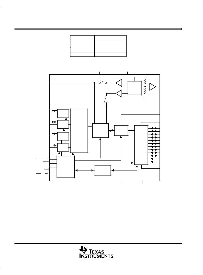
functional block diagram |
|
|
|
|
|
|
|
|
|
|
|
|
AVDD |
|
DVDD |
|
|
REFP |
|
|
|
|
3.5 V |
|
|
2.5 V |
|
|
|
|
|
|
1.225 V |
|
|
|
|
|
|
|
|
|
REFOUT |
|
|
|
|
|
|
1.5 V |
|
REF |
|
|
|
|
|
|
|
|
|
|
REFM |
|
|
|
|
|
|
|
|
REFIN |
|
|
|
|
|
|
|
|
AINP |
S/H |
|
|
|
VREFM |
|
|
DATA_AV |
|
|
|
|
VREFP |
|
|
|
|
|
|
|
|
|
|
|
|
|
AINM |
S/H |
Single |
+ |
|
|
|
|
BVDD |
10 Bit |
|
|
|
|
||||
|
|
Ended |
|
10 |
FIFO |
10 |
D0 |
|
|
|
and/or |
|
Pipeline |
||||
|
|
± |
|
16 × 10 |
|
D1 |
||
|
|
Differential |
ADC |
|
|
|||
BINP |
S/H |
|
|
|
|
D2 |
||
MUX |
|
|
|
|
|
|||
|
|
|
|
Buffers |
D3 |
|||
|
|
|
|
|
|
|
||
|
|
|
|
|
|
|
D4 |
|
|
|
|
|
|
|
|
|
|
|
|
|
|
|
|
|
|
D5 |
BINM |
S/H |
|
|
|
|
|
|
D6 |
|
|
|
|
|
|
|
|
D7 |
|
|
|
|
|
|
|
|
D8 |
|
|
|
|
|
|
|
|
D9 |
CONV_CLK (CONVST) |
|
|
|
|
|
|
|
RA0 |
CS0 |
Logic |
|
|
|
|
|
|
RA1 |
|
|
|
|
|
|
|
||
CS1 |
and |
|
|
Control |
|
|
BGND |
|
RD |
Control |
|
|
|
|
|||
|
|
Register |
|
|
|
|||
WR (R/W) |
|
|
|
|
|
|
|
|
|
|
|
|
|
|
AGND |
DGND |
|
2 |
POST OFFICE BOX 655303 •DALLAS, TEXAS 75265 |

|
|
|
|
|
|
|
|
|
|
|
|
|
|
|
THS10064 |
|
|
|
|
|
|
|
|
|
|
|
|
|
|
10-BIT 6 MSPS, SIMULTANEOUS SAMPLING |
|||
|
|
|
|
|
|
|
|
|
|
|
|
|
|
|
ANALOG-TO-DIGITAL CONVERTER |
|
|
|
|
|
|
|
|
|
|
|
|
|
|
|
|
SLAS255 ± DECEMBER 1999 |
|
|
|
|
|
|
|
|
|
|
|
|
|
|
|
|
|
|
|
|
|
|
|
|
|
|
|
|
|
|
Terminal Functions |
||||
|
|
|
|
|
|
|
|
|
|
|
|
|
|
|
|
|
|
|
|
|
|
|
TERMINAL |
|
I/O |
|
|
|
|
DESCRIPTION |
|
||
|
|
|
|
|
NAME |
NO. |
|
|
|
|
|
|||||
|
|
|
|
|
|
|
|
|
|
|
|
|||||
|
|
|
|
|
|
|
|
|
|
|
|
|
|
|
|
|
|
AINP |
32 |
I |
Analog input, single-ended or positive input of differential channel A |
|
|||||||||||
|
|
|
|
|
|
|
|
|
|
|
|
|
|
|
|
|
|
AINM |
31 |
I |
Analog input, single-ended or negative input of differential channel A |
|
|||||||||||
|
|
|
|
|
|
|
|
|
|
|
|
|
|
|
|
|
|
BINP |
30 |
I |
Analog input, single-ended or positive input of differential channel B |
|
|||||||||||
|
|
|
|
|
|
|
|
|
|
|
|
|
|
|
|
|
|
BINM |
29 |
I |
Analog input, single-ended or negative input of differential channel B |
|
|||||||||||
|
|
|
|
|
|
|
|
|
|
|
|
|
|
|
|
|
|
AVDD |
23 |
I |
Analog supply voltage |
|
|||||||||||
|
AGND |
24 |
I |
Analog ground |
|
|||||||||||
|
|
|
|
|
|
|
|
|
|
|
|
|
|
|
|
|
|
BVDD |
7 |
I |
Digital supply voltage for buffer |
|
|||||||||||
|
BGND |
8 |
I |
Digital ground for buffer |
|
|||||||||||
|
|
|
|
|
|
|
|
|
|
|
|
|
|
|
||
|
CONV_CLK |
|
|
15 |
I |
Digital input. This input is used to apply an external conversion clock in continuous conversion |
|
|||||||||
|
(CONVST) |
|
|
|||||||||||||
|
|
|
|
|
|
|
|
|
|
|
mode. In single conversion mode, this input functions as the conversion start (CONVST) input. |
|
||||
|
|
|
|
|
|
|
|
|
|
|
A high to low transition on this input holds simultaneously the selected analog input channels |
|
||||
|
|
|
|
|
|
|
|
|
|
|
and initiates a single conversion of all selected analog inputs. |
|
||||
|
|
|
|
|
|
|
|
|
|
|
|
|
|
|||
|
|
|
|
|
|
|
|
|
22 |
I |
Chip select input (active low) |
|
||||
|
CS0 |
|
|
|
|
|||||||||||
|
|
|
|
|
|
|
|
|
|
|
|
|
|
|||
|
CS1 |
21 |
I |
Chip select input (active high) |
|
|||||||||||
|
|
|
|
|
|
|
|
|
|
|
|
|
|
|||
|
DATA_AV |
16 |
O |
Data available signal, which can be used to generate an interrupt for processors and as a level |
|
|||||||||||
|
|
|
|
|
|
|
|
|
|
|
information of the internal FIFO. This signal can be configured to be active low or high and can |
|
||||
|
|
|
|
|
|
|
|
|
|
|
be configured as a static level or pulse output. See Table 14. |
|
||||
|
|
|
|
|
|
|
|
|
|
|
|
|
|
|||
|
DGND |
17 |
I |
Digital ground. Ground reference for digital circuitry. |
|
|||||||||||
|
|
|
|
|
|
|
|
|
|
|
|
|
|
|||
|
DVDD |
18 |
I |
Digital supply voltage |
|
|||||||||||
|
D0 ± D9 |
1±6, 9±12 |
I/O/Z |
Digital input, output; D0 = LSB |
|
|||||||||||
|
|
|
|
|
|
|
|
|
|
|
|
|
|
|||
|
RA0 |
13 |
I |
Digital input. RA0 is used as an address line for the control register. This is required for writing |
|
|||||||||||
|
|
|
|
|
|
|
|
|
|
|
to the control register 0 and control register 1. See Table 8. |
|
||||
|
|
|
|
|
|
|
|
|
|
|
|
|
|
|||
|
RA1 |
14 |
I |
Digital input. RA1 is used as an address line for the control register. This is required for writing |
|
|||||||||||
|
|
|
|
|
|
|
|
|
|
|
to control register 0 and control register 1. See Table 8. |
|
||||
|
|
|
|
|
|
|
|
|
|
|
|
|
|
|||
|
REFIN |
28 |
I |
Common-mode reference input for the analog input channels. It is recommended that this pin |
|
|||||||||||
|
|
|
|
|
|
|
|
|
|
|
be connected to the reference output REFOUT. |
|
||||
|
|
|
|
|
|
|
|
|
|
|
|
|
|
|||
|
REFP |
26 |
I |
Reference input, requires a bypass capacitor of 10 F to AGND in order to bypass the internal |
|
|||||||||||
|
|
|
|
|
|
|
|
|
|
|
reference voltage. An external reference voltage at this input can be applied. This option can |
|
||||
|
|
|
|
|
|
|
|
|
|
|
be programmed through control register 0. See Table 9. |
|
||||
|
|
|
|
|
|
|
|
|
|
|
|
|
|
|||
|
REFM |
25 |
I |
Reference input, requires a bypass capacitor of 10 F to AGND in order to bypass the internal |
|
|||||||||||
|
|
|
|
|
|
|
|
|
|
|
reference voltage. An external reference voltage at this input can be applied. This option can |
|
||||
|
|
|
|
|
|
|
|
|
|
|
be programmed through control register 0. See Table 9. |
|
||||
|
|
|
|
|
|
|
|
|
|
|
|
|
|
|||
|
REFOUT |
27 |
O |
Analog fixed reference output voltage of 2.5 V. Sink and source capability of 250 A. The |
|
|||||||||||
|
|
|
|
|
|
|
|
|
|
|
reference output requires a capacitor of 10 F to AGND for filtering and stability. |
|
||||
|
|
|
|
|
|
|
|
|
|
|
|
|
|
|||
|
|
² |
|
|
19 |
I |
The |
|
input is used only if the |
|
input is configured as a write only input. In this case, it is a |
|
||||
|
RD |
RD |
WR |
|
||||||||||||
|
|
|
|
|
|
|
|
|
|
|
digital input, active low as a data read select from the processor. See timing section. |
|
||||
|
|
|
|
|
|
|
|
|||||||||
|
|
|
|
|
|
² |
20 |
I |
This input is programmable. It functions as a read-write input R/W and can also be configured |
|
||||||
|
WR |
(R/W) |
|
|||||||||||||
|
|
|
|
|
|
|
|
|
|
|
as a write-only input WR, which is active low and used as data write select from the processor. |
|
||||
|
|
|
|
|
|
|
|
|
|
|
In this case, the RD input is used as a read input from the processor. See timing section. |
|
||||
|
|
|
|
|
|
|
|
|
|
|
|
|
|
|
|
|
² The start-conditions of RD and WR (R/W) are unknown. The first access to the ADC has to be a write access to initialize the ADC.
POST OFFICE BOX 655303 •DALLAS, TEXAS 75265 |
3 |

THS10064
10-BIT 6 MSPS, SIMULTANEOUS SAMPLING ANALOG-TO-DIGITAL CONVERTER
SLAS255 ± DECEMBER 1999
absolute maximum ratings over operating free-air temperature (unless otherwise noted)²
Supply voltage range, DGND to DVDD . . . . . . . . . . . . . . . . . . . . . . . . . . . . . . . |
. . . . . . . . . . . . . . . ±0.3 V to 6.5 V |
BGND to BVDD . . . . . . . . . . . . . . . . . . . . . . . . . . . . . . . . |
. . . . . . . . . . . . . . ±0.3 V to 6.5 V |
AGND to AVDD . . . . . . . . . . . . . . . . . . . . . . . . . . . . . . . . . |
. . . . . . . . . . . . . . ±0.3 V to 6.5 V |
Analog input voltage range . . . . . . . . . . . . . . . . . . . . . . . . . . . . . . . . . . . . . . . . . . |
AGND ± 0.3 V to AVDD + 1.5 V |
Reference input voltage . . . . . . . . . . . . . . . . . . . . . . . . . . . . . . . . . . . . . . . . . . . . |
±0.3 + AGND to AVDD + 0.3 V |
Digital input voltage range . . . . . . . . . . . . . . . . . . . . . . . . . . . . . . . . . . . . . . . . . . . |
±0.3 V to BVDD/DVDD + 0.3 V |
Operating virtual junction temperature range, TJ . . . . . . . . . . . . . . . . . . . . . . . . |
. . . . . . . . . . . . . ±40°C to 150°C |
Operating free-air temperature range,TA THS10064C . . . . . . . . . . . . . . . . . . |
. . . . . . . . . . . . . . . . 0°C to 70°C |
THS10064I . . . . . . . . . . . . . . . . . . . |
. . . . . . . . . . . . . . ±40°C to 85°C |
Storage temperature range, Tstg . . . . . . . . . . . . . . . . . . . . . . . . . . . . . . . . . . . . . . |
. . . . . . . . . . . . . ±65°C to 150°C |
Lead temperature 1,6 mm (1/16 inch) from case for 10 seconds . . . . . . . . . . |
. . . . . . . . . . . . . . . . . . . . . 260°C |
²Stresses beyond those listed under ªabsolute maximum ratingsº may cause permanent damage to the device. These are stress ratings only, and functional operation of the device at these or any other conditions beyond those indicated under ªrecommended operating conditionsº is not implied. Exposure to absolute-maximum-rated conditions for extended periods may affect device reliability.
recommended operating conditions power supply
|
|
MIN |
NOM |
MAX |
UNIT |
|
|
|
|
|
|
|
AVDD |
4.75 |
5 |
5.25 |
|
Supply voltage |
DVDD |
3 |
3.3 |
5.25 |
V |
|
BVDD |
3 |
3.3 |
5.25 |
|
analog and reference inputs
|
MIN |
NOM |
MAX |
UNIT |
|
|
|
|
|
Analog input voltage in single-ended configuration |
VREFM |
|
VREFP |
V |
Common-mode input voltage VCM in differential configuration |
1 |
2.5 |
4 |
V |
External reference voltage,VREFP (optional) |
|
3.5 |
AVDD±1.2 |
V |
External reference voltage, VREFM (optional) |
1.4 |
1.5 |
|
V |
Input voltage difference, REFP ± REFM |
|
2 |
|
V |
digital inputs
|
|
MIN |
NOM |
MAX |
UNIT |
|
|
|
|
|
|
High-level input voltage, VIH |
BVDD = 3.3 V |
2 |
|
|
V |
BVDD = 5.25 V |
2.6 |
|
|
V |
|
|
|
|
|||
Low-level input voltage, VIL |
BVDD = 3.3 V |
|
|
0.6 |
V |
BVDD = 5.25 V |
|
|
0.6 |
V |
|
|
|
|
|||
Input CONV_CLK frequency |
DVDD = 3 V to 5.25 V |
0.1 |
|
6 |
MHz |
CONV_CLK pulse duration, clock high, tw(CONV_CLKH) |
DVDD = 3 V to 5.25 V |
80 |
83 |
5000 |
ns |
CONV_CLK pulse duration, clock low, tw(CONV_CLKL) |
DVDD = 3 V to 5.25 V |
80 |
83 |
5000 |
ns |
Operating free-air temperature, TA |
THS10064CDA |
0 |
|
70 |
°C |
|
|
|
|
||
THS10064IDA |
±40 |
|
85 |
||
|
|
|
4 |
POST OFFICE BOX 655303 •DALLAS, TEXAS 75265 |

THS10064 10-BIT 6 MSPS, SIMULTANEOUS SAMPLING ANALOG-TO-DIGITAL CONVERTER
SLAS255 ± DECEMBER 1999
electrical characteristics over recommended operating conditions, DVDD = 3.3 V, AVDD = 5 V, VREF = internal (unless otherwise noted)
digital specifications
|
PARAMETER |
TEST CONDITIONS |
MIN |
TYP MAX |
UNIT |
|
|
|
|
|
|
|
|
Digital inputs |
|
|
|
|
|
|
|
|
|
|
|
|
|
IIH |
High-level input current |
DVDD = digital inputs |
±50 |
50 |
A |
|
IIL |
Low-level input current |
Digital input = 0 V |
±50 |
50 |
A |
|
Ci |
Input capacitance |
|
|
|
5 |
pF |
Digital outputs |
|
|
|
|
|
|
|
|
|
|
|
|
|
VOH |
High-level output voltage |
IOH = ±50 A, |
BVDD = 3.3 V, 5 V |
BVDD±0.5 |
|
V |
VOL |
Low-level output voltage |
IOL = 50 A, |
BVDD = 3.3 V, 5 V |
|
0.4 |
V |
IOZ |
High-impedance-state output current |
CS1 = DGND, |
CS0 = DVDD |
±10 |
10 |
A |
CO |
Output capacitance |
|
|
|
5 |
pF |
CL |
Load capacitance at databus D0 ± D11 |
|
|
|
30 |
pF |
POST OFFICE BOX 655303 •DALLAS, TEXAS 75265 |
5 |

THS10064
10-BIT 6 MSPS, SIMULTANEOUS SAMPLING ANALOG-TO-DIGITAL CONVERTER
SLAS255 ± DECEMBER 1999
electrical characteristics over recommended operating conditions, AVDD = 5 V,
DVDD = BVDD = 3.3 V, fs = 6 MSPS, VREF = internal (unless otherwise noted) (continued)
dc specifications
|
PARAMETER |
TEST CONDITIONS |
MIN |
TYP |
MAX |
UNIT |
|
|
|
|
|
|
|
|
Resolution |
|
10 |
|
|
Bits |
|
|
|
|
|
|
|
Accuracy |
|
|
|
|
|
|
|
|
|
|
|
|
|
|
Integral nonlinearity, INL |
|
|
|
±1 |
LSB |
|
|
|
|
|
|
|
|
Differential nonlinearity, DNL |
|
|
|
±1 |
LSB |
|
|
|
|
|
|
|
|
Offset error |
After calibration in single-ended mode |
±15 |
|
15 |
mV |
|
|
|
|
|
|
|
|
After calibration in differential mode |
±5 |
|
5 |
mV |
|
|
|
|
||||
|
|
|
|
|
|
|
|
Gain error |
|
|
|
1% |
FSR |
|
|
|
|
|
|
|
Analog input |
|
|
|
|
|
|
|
|
|
|
|
|
|
|
Input capacitance |
|
|
15 |
|
pF |
|
|
|
|
|
|
|
|
Input leakage current |
VAIN = VREFM to VREFP |
|
|
±10 |
A |
Internal voltage reference |
|
|
|
|
|
|
|
|
|
|
|
|
|
|
Accuracy, VREFP |
|
3.33 |
3.5 |
3.67 |
V |
|
Accuracy, VREFM |
|
1.42 |
1.5 |
1.58 |
V |
|
Temperature coefficient |
|
|
50 |
|
PPM/°C |
|
|
|
|
|
|
|
|
Reference noise |
|
|
100 |
|
V |
|
|
|
|
|
|
|
|
Accuracy, REFOUT |
|
2.475 |
2.5 |
2.525 |
V |
|
|
|
|
|
|
|
Power supply |
|
|
|
|
|
|
|
|
|
|
|
|
|
IDDA |
Analog supply current |
AVDD =5 V, BVDD = DVDD = 3.3 V |
|
36 |
40 |
mA |
IDDD |
Digital supply voltage |
AVDD = 5 V, BVDD = DVDD = 3.3 V |
|
0.5 |
1 |
mA |
IDDB |
Buffer supply voltage |
AVDD = 5 V, BVDD = DVDD = 3.3 V |
|
1.5 |
4 |
mA |
IDD_P |
Supply current in power-down mode |
AVDD = 5 V, BVDD = DVDD = 3.3 V |
|
|
7 |
mA |
|
Power dissipation |
AVDD = 5 V, DVDD = BVDD = 3.3 V |
|
186 |
216 |
mW |
|
Power dissipation in power down |
AVDD = 5 V, DVDD = BVDD = 3.3 V |
|
30 |
|
mW |
6 |
POST OFFICE BOX 655303 •DALLAS, TEXAS 75265 |

THS10064 10-BIT 6 MSPS, SIMULTANEOUS SAMPLING ANALOG-TO-DIGITAL CONVERTER
SLAS255 ± DECEMBER 1999
electrical characteristics over recommended operating conditions, VREF = internal, fs = 6 MHz, fI = 2 MHz at ±1dBFS (unless otherwise noted) (continued)
ac specifications, AVDD = 5 V, BVDD = DVDD = 3.3 V, CL < 30 pF
|
PARAMETER |
TEST CONDITIONS |
MIN |
TYP |
MAX |
UNIT |
|
|
|
|
|
|
|
|
|
Differential mode |
56 |
59 |
|
dB |
SINAD |
Signal-to-noise ratio + distortion |
|
|
|
|
|
Single-ended mode |
|
59 |
|
dB |
||
|
|
(see Note 1) |
|
|
||
|
|
|
|
|
|
|
|
|
|
|
|
|
|
|
|
Differential mode |
59 |
61 |
|
dB |
SNR |
Signal-to-noise ratio |
|
|
|
|
|
Single-ended mode |
|
60 |
|
dB |
||
|
|
(see Note 1) |
|
|
||
|
|
|
|
|
|
|
|
|
|
|
|
|
|
THD |
Total harmonic distortion |
Differential mode |
|
±67 |
±61 |
dB |
|
|
|
|
|
||
Single-ended mode |
|
±67 |
|
dB |
||
|
|
|
|
|||
|
|
|
|
|
|
|
ENOB |
|
Differential mode |
9 |
9.6 |
|
Bits |
Effective number of bits |
|
|
|
|
|
|
Single-ended mode |
|
|
|
|
||
(SNR) |
|
9.5 |
|
Bits |
||
|
(see Note 1) |
|
|
|||
|
|
|
|
|
|
|
|
|
|
|
|
|
|
SFDR |
Spurious free dynamic range |
Differential mode |
61 |
68 |
|
dB |
|
|
|
|
|
||
Single-ended mode |
|
68 |
|
dB |
||
|
|
|
|
|||
|
|
|
|
|
|
|
Analog Input |
|
|
|
|
|
|
|
|
|
|
|
|
|
|
Full-power bandwidth with a source impedance of 150 Ω in |
Full scale sinewave, ±3 dB |
|
96 |
|
MHz |
|
differential configuration. |
|
|
|||
|
|
|
|
|
|
|
|
|
|
|
|
|
|
|
Full-power bandwidth with a source impedance of 150 Ω in |
Full scale sinewave, ±3 dB |
|
54 |
|
MHz |
|
single-ended configuration. |
|
|
|||
|
|
|
|
|
|
|
|
|
|
|
|
|
|
|
Small-signal bandwidth with a source impedance of 150 Ω in |
100 mVpp sinewave, ±3 dB |
|
96 |
|
MHz |
|
differential configuration. |
|
|
|||
|
|
|
|
|
|
|
|
|
|
|
|
|
|
|
Small-signal bandwidth with a source impedance of 150 Ω in |
100 mVpp sinewave, ±3 dB |
|
54 |
|
MHz |
|
single-ended configuration. |
|
|
|||
|
|
|
|
|
|
|
|
|
|
|
|
|
|
NOTE 1: The SNR (ENOB) and SINAD is degraded typically by 2 dB in single-ended mode when the reading of data is asynchronous to the sampling clock.
POST OFFICE BOX 655303 •DALLAS, TEXAS 75265 |
7 |

THS10064
10-BIT 6 MSPS, SIMULTANEOUS SAMPLING ANALOG-TO-DIGITAL CONVERTER
SLAS255 ± DECEMBER 1999
timing specifications, AVDD = 5 V, BVDD = DVDD = 3.3 V, VREF = internal, CL < 30 pF
|
PARAMETER |
TEST CONDITIONS |
MIN TYP MAX |
UNIT |
|
|
|
|
|
td(DATA_AV) |
Delay time |
|
5 |
ns |
td(o) |
Delay time |
|
5 |
ns |
tpipe |
Latency |
|
5 |
CONV |
|
CLK |
|||
|
|
|
|
|
|
|
|
|
|
timing specification of the single conversion mode²
|
PARAMETER |
TEST CONDITIONS |
MIN |
TYP |
MAX |
UNIT |
|||
|
|
|
|
|
|
|
|
|
|
tc |
Clock cycle of the internal clock oscillator |
|
|
159 |
167 |
175 |
ns |
||
tw1 |
Pulse width, |
|
|
|
|
1.5×tc |
|
|
ns |
CONVST |
|
|
|
|
|
||||
tdA |
Aperture time |
|
|
|
1 |
|
ns |
||
|
|
|
|
1 analog input |
|
2×tc |
|
|
ns |
t2 |
Time between consecutive start of single conversion |
2 analog inputs |
|
3×tc |
|
|
|||
|
|
|
|
||||||
3 analog inputs |
|
4×tc |
|
|
ns |
||||
|
|
|
|
|
|
|
|||
|
|
|
|
4 analog inputs |
|
5×tc |
|
|
|
|
|
|
|
|
|
|
|
||
|
|
|
|
1 analog input, |
TL = 1 |
|
|
6×tc |
ns |
|
Delay time, DATA_AV becomes active for the trigger |
2 analog inputs, TL = 2 |
|
|
7×tc |
||||
|
|
|
|
||||||
|
level condition: TRIG0 = 0, TRIG1 = 0 |
3 analog inputs, TL = 3 |
|
|
8×tc |
ns |
|||
|
|
|
|
4 analog inputs, |
TL = 4 |
|
|
9×tc |
|
|
|
|
|
|
|
|
|||
|
|
|
|
1 analog input, |
TL = 4 |
|
|
3×t2 +6×tc |
ns |
td(DATA_AV) |
Delay time, DATA_AV becomes active for the trigger |
2 analog inputs, |
TL = 4 |
|
|
t2 +7×tc |
|||
|
|
|
|||||||
level condition: TRIG0 = 1, TRIG1 = 0 |
3 analog inputs, |
TL = 6 |
|
|
t2 +8×tc |
ns |
|||
|
|
|
|||||||
|
|
|
|
4 analog inputs, |
TL = 8 |
|
|
t2 +9×tc |
|
|
|
|
|
|
|
|
|||
|
|
|
|
1 analog input, |
TL = 8 |
|
|
7×t2 +6×tc |
ns |
|
Delay time, DATA_AV becomes active for the trigger |
2 analog inputs, TL = 8 |
|
|
3×t2 +7×tc |
||||
|
|
|
|
||||||
|
level condition: TRIG0 = 0, TRIG1 = 1 |
3 analog inputs, TL = 9 |
|
|
2×t2 +8×tc |
ns |
|||
|
|
|
|
4 analog inputs, |
TL = 12 |
|
|
2×t2 +9×tc |
|
|
|
|
|
|
|
|
|||
|
Delay time, DATA_AV becomes active for the trigger |
1 analog input, |
TL = 14 |
|
|
13×t2 +6×tc |
ns |
||
td(DATA_AV) |
2 analog inputs, TL = 12 |
|
|
5×t2 +7×tc |
|||||
level condition: TRIG0 = 1, TRIG1 = 1 |
|
|
|
||||||
|
3 analog inputs, TL = 12 |
|
|
3×t2 +8×tc |
ns |
||||
|
|
|
|
|
|
||||
² Timing parameters are ensured by design but are not tested.
8 |
POST OFFICE BOX 655303 •DALLAS, TEXAS 75265 |

THS10064 10-BIT 6 MSPS, SIMULTANEOUS SAMPLING ANALOG-TO-DIGITAL CONVERTER
SLAS255 ± DECEMBER 1999
detailed description
reference voltage
The THS10064 has a built-in reference, which provides the reference voltages for the ADC. VREFP is set to 3.5 V and VREFM is set to 1.5 V. An external reference can also be used through two reference input pins, REFP and REFM, if the reference source is programmed as external. The voltage levels applied to these pins establish the upper and lower limits of the analog inputs to produce a full-scale and zero-scale reading respectively.
analog inputs
The THS10064 consists of 4 analog inputs, which are sampled simultaneously. These inputs can be selected individually and configured as single-ended or differential inputs. The desired analog input channel can be programmed.
analog-to-digital converter
The THS10064 uses a 10-bit pipelined multistaged architecture with 4 1-bit stages followed by 4 2-bit stages, which achieves a high sample rate with low power consumption. The THS10064 distributes the conversion over several smaller ADC sub-blocks, refining the conversion with progressively higher accuracy as the device passes the results from stage to stage. This distributed conversion requires a small fraction of the number of comparators used in a traditional flash ADC. A sample-and-hold amplifier (SHA) within each of the stages permits the first stage to operate on a new input sample while the second through the eighth stages operate on the seven preceding samples.
conversion modes
The conversion can be performed in two different conversion modes. In the single conversion mode, the conversion is initiated by an external signal (CONVST). An internal oscillator controls the conversion time. In the continuous conversion mode, an external clock signal is applied to the clock input (CONV_CLK). A new conversion is started with every falling edge of the applied clock signal.
sampling rate
The maximum possible conversion rate per channel is dependent on the selected analog input channels. Table 1 shows the maximum conversion rate in the continuous conversion mode for different combinations.
Table 1. Maximum Conversion Rate in Continuous Conversion Mode
CHANNEL CONFIGURATION |
NUMBER OF |
MAXIMUM CONVERSION |
|
CHANNELS |
RATE PER CHANNEL |
||
|
|||
|
|
|
|
1 single-ended channel |
1 |
6 MSPS |
|
|
|
|
|
2 single-ended channels |
2 |
3 MSPS |
|
|
|
|
|
3 single-ended channels |
3 |
2 MSPS |
|
|
|
|
|
4 single-ended channels |
4 |
1.5 MSPS |
|
|
|
|
|
1 differential channel |
1 |
6 MSPS |
|
|
|
|
|
2 differential channels |
2 |
3 MSPS |
|
|
|
|
|
1 single-ended and 1 differential channel |
2 |
3 MSPS |
|
|
|
|
|
2 single-ended and 1 differential channels |
3 |
2 MSPS |
The maximum conversion rate in the continuous conversion mode per channel, fc, is given by:
fc + #6channelsMSPS
Table 2 shows the maximum conversion rate in the single conversion mode.
POST OFFICE BOX 655303 •DALLAS, TEXAS 75265 |
9 |
THS10064
10-BIT 6 MSPS, SIMULTANEOUS SAMPLING ANALOG-TO-DIGITAL CONVERTER
SLAS255 ± DECEMBER 1999
sampling rate (continued)
Table 2. Maximum Conversion Rate in Single Conversion Mode
CHANNEL CONFIGURATION |
NUMBER OF |
MAXIMUM CONVERSION |
|
CHANNELS |
RATE PER CHANNEL |
||
|
|||
|
|
|
|
1 single-ended channel |
1 |
3 MSPS |
|
|
|
|
|
2 single-ended channels |
2 |
2 MSPS |
|
|
|
|
|
3 single-ended channels |
3 |
1.5 MSPS |
|
|
|
|
|
4 single-ended channels |
4 |
1.2 MSPS |
|
|
|
|
|
1 differential channel |
1 |
3 MSPS |
|
|
|
|
|
2 differential channels |
2 |
2 MSPS |
|
|
|
|
|
1 single-ended and 1 differential channel |
2 |
1.5 MSPS |
|
|
|
|
|
2 single-ended and 1 differential channels |
3 |
1.2 MSPS |
single conversion mode
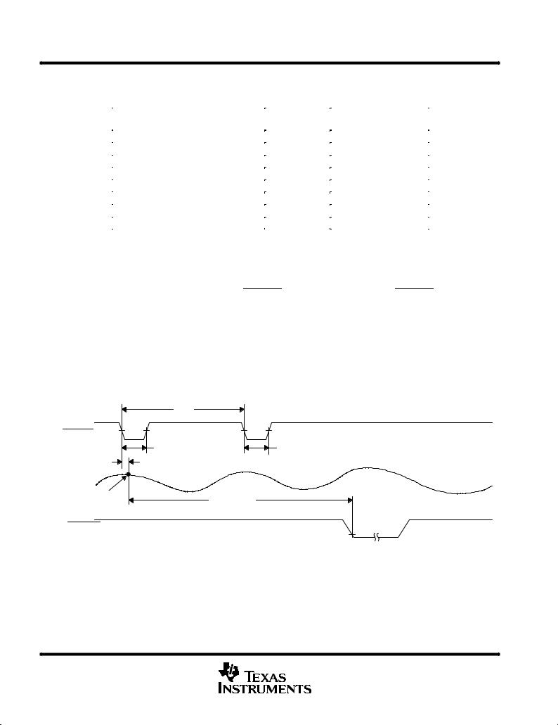
In single conversion mode, a single conversion of the selected analog input channels is performed. The single conversion mode is selected by setting bit 1 of control register 0 to 1.
A single conversion is initiated by pulsing the CONVST input. On the falling edge of CONVST, the sample and hold stages of the selected analog inputs are placed into hold simultaneously, and the conversion sequence for the selected channels is started.
The conversion clock in single conversion mode is generated internally using a clock oscillator circuit. The signal DATA_AV (data available) becomes active when the trigger level is reached and indicates that the converted sample(s) is (are) written into the FIFO and can be read out. The trigger level in the single conversion mode can be selected according to Table 13.
Figure 1 shows the timing of the single conversion mode. In this mode, up to four analog input channels can be selected to be sampled simultaneously (see Table 2).
t2
CONVST
t1 |
t1 |
td(A)
AIN
Sample N
tDATA_AV
DATA_AV,
Trigger Level = 1
Figure 1. Timing of Single Conversion Mode
The time (t2) between consecutive starts of single conversions is dependent on the number of selected analog
input channels. The time tDATA_AV, until DATA_AV becomes active is given by: tDATA_AV = tpipe + n ×tc. This equation is valid for a trigger level which is equivalent to the number of selected analog input channels. For all
other trigger level conditions refer to the timing specifications of single conversion mode.
10 |
POST OFFICE BOX 655303 •DALLAS, TEXAS 75265 |

THS10064 10-BIT 6 MSPS, SIMULTANEOUS SAMPLING ANALOG-TO-DIGITAL CONVERTER
SLAS255 ± DECEMBER 1999
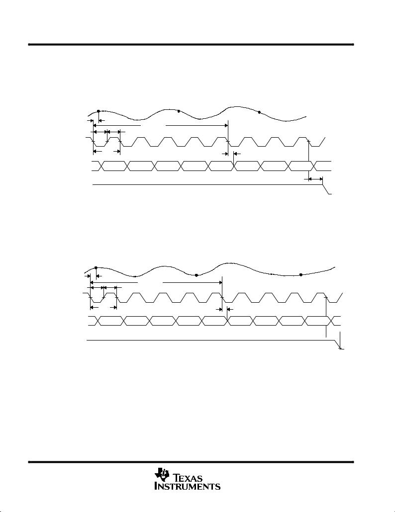
continuous conversion mode
The internal clock oscillator used in the single-conversion mode is switched off in continuous conversion mode. In continuous conversion mode, (bit 1 of control register 0 set to 0) the ADC operates with a free running external clock signal CONV_CLK. With every rising edge of the CONV_CLK signal a new converted value is written into the FIFO. The first conversion value is written into the FIFO with a latency of 8 + TL (trigger level) clock cycles after the FIFO reset.
Figure 2 shows the timing of continuous conversion mode when one analog input channel is selected. The maximum throughput rate is 6 MSPS in this mode. The timing of the DATA_AV signal is shown here in the case of a trigger level set to 1 or 4.
Sample N |
Sample N+1 |
Sample N+2 |
Sample N+3 |
Sample N+4 |
Sample N+5 |
Sample N+6 |
Sample N+7 |
Sample N+8 |
Channel 1 |
Channel 1 |
Channel 1 |
Channel 1 |
Channel 1 |
Channel 1 |
Channel 1 |
Channel 1 |
Channel 1 |
AIN |
|
|
|
|
|
|
|
|
|
|
td(A) |
td(pipe) |
|
|
|
|
|
|
|
|
|
|
|
|
|
|
|
||
tw(CONV_CLKH) |
|
tw(CONV_CLKL) |
|
|
|
|
|
|
|
50% |
50% |
|
|
|
|
|
|
|
|
CONV_CLK |
|
|
|
|
|
|
|
|
|
|
tc |
|
|
|
td(O) |
|
|
|
|
Data Into |
Data N±5 |
Data N±4 |
Data N±3 |
Data N±2 |
Data N±1 |
Data N |
Data N+1 |
Data N+2 |
Data N+3 |
FIFO |
Channel 1 |
Channel 1 |
Channel 1 |
Channel 1 |
Channel 1 |
Channel 1 |
Channel 1 |
Channel 1 |
Channel 1 |
td(DATA_AV)
DATA_AV,
Trigger Level = 1
td(DATA_AV)
DATA_AV,
Trigger Level = 4
Figure 2. Timing of Continuous Conversion Mode (1-channel operation)
Figure 3 shows the timing of continuous conversion mode when two analog input channels are selected. The maximum throughput rate per channel is 3 MSPS in this mode. The data flow in the bottom of the figure shows the order the converted data is written into the FIFO. The timing of the DATA_AV signal shown here is for a trigger level set to 2 or 4.
Sample N |
Sample N+1 |
Sample N+2 |
Sample N+3 |
Sample N+4 |
|||||
Channel 1,2 |
Channel 1,2 |
Channel 1,2 |
Channel 1,2 |
Channel 1,2 |
|||||
AIN |
|
|
|
|
|
|
|
|
|
|
td(A) |
td(Pipe) |
|
|
|
|
|
|
|
tw(CONV_CLKH) |
|
tw(CONV_CLKL) |
|
|
|
|
|
|
|
50% |
50% |
|
|
|
|
|
|
|
|
CONV_CLK |
|
|
|
|
|
|
|
|
|
|
tc |
|
|
|
td(O) |
|
|
|
|
Data Into |
Data N±3 |
Data N±2 |
Data N±2 |
Data N±1 |
Data N±1 |
Data N |
Data N |
Data N+1 |
Data N+1 |
FIFO |
Channel 2 |
Channel 1 |
Channel 2 |
Channel 1 |
Channel 2 |
Channel 1 |
Channel 2 |
Channel 1 |
Channel 2 |
td(DATA_AV)
DATA_AV,
Trigger Level = 2
td(DATA_AV)
DATA_AV,
Trigger Level = 4
Figure 3. Timing of Continuous Conversion Mode (2-channel operation)
POST OFFICE BOX 655303 •DALLAS, TEXAS 75265 |
11 |
THS10064
10-BIT 6 MSPS, SIMULTANEOUS SAMPLING ANALOG-TO-DIGITAL CONVERTER
SLAS255 ± DECEMBER 1999
continuous conversion mode (continued)
Figure 4 shows the timing of continuous conversion mode when three analog input channels are selected. The maximum throughput rate per channel is 2 MSPS in this mode. The data flow in the bottom of the figure shows in which order the converted data is written into the FIFO. The timing of the DATA_AV signal shown here is for a trigger level set to 3.
Sample N |
Sample N+1 |
Sample N+2 |
Channel 1,2,3 |
Channel 1,2,3 |
Channel 1,2,3 |
AIN |
|
|
|
|
|
|
|
|
|
td(A) |
td(Pipe) |
|
|
|
|
|
|
|
|
|
|
|
|
|
||
tw(CONV_CLKH) |
|
tw(CONV_CLKL) |
|
|
|
|
|
|
50% |
50% |
|
|
|
|
|
|
|
CONV_CLK |
|
|
|
|
|
|
|
|
|
tc |
|
|
|
td(O) |
|
|
|
|
|
|
|
|
|
|
|
|
Data Into |
Data N±2 |
Data N±2 |
Data N±1 |
Data N±1 |
Data N±1 |
Data N |
Data N |
Data N |
FIFO |
Channel 2 |
Channel 3 |
Channel 1 |
Channel 2 |
Channel 3 |
Channel 1 |
Channel 2 |
Channel 3 |
td(DATA_AV)
DATA_AV,
Trigger Level = 3
Figure 4. Timing of Continuous Conversion Mode (3-channel operation)
Figure 5 shows the timing of continuous conversion mode when four analog input channels are selected. The maximum throughput rate per channel is 1.5 MSPS in this mode. The data flow in the bottom of the figure shows in which order the converted data is written into the FIFO. The timing of the DATA_AV signal shown here is for a trigger level of 4.
Sample N |
Sample N+1 |
Sample N+2 |
Channel 1,2,3,4 |
Channel 1,2,3,4 |
Channel 1,2,3,4 |
AIN |
|
|
|
|
|
|
|
|
|
|
td(A) |
td(Pipe) |
|
|
|
|
|
|
|
tw(CONV_CLKH) |
|
|
|
|
|
|
|
||
|
tw(CONV_CLKL) |
|
|
|
|
|
|
||
50% |
50% |
|
|
|
|
|
|
|
|
CONV_CLK |
|
|
|
|
|
|
|
|
|
|
tc |
|
|
|
td(O) |
|
|
|
|
Data Into |
Data N±2 |
Data N±1 |
Data N±1 |
Data N±1 |
Data N±1 |
Data N |
Data N |
Data N |
Data N |
FIFO |
Channel 4 |
Channel 1 |
Channel 2 |
Channel 3 |
Channel 4 |
Channel 1 |
Channel 2 |
Channel 3 |
Channel 4 |
td(DATA_AV) 
DATA_AV,
Trigger Level = 4
Figure 5. Timing of Continuous Conversion Mode (4-channel operation)
12 |
POST OFFICE BOX 655303 •DALLAS, TEXAS 75265 |
THS10064 10-BIT 6 MSPS, SIMULTANEOUS SAMPLING ANALOG-TO-DIGITAL CONVERTER
SLAS255 ± DECEMBER 1999
digital output data format
The digital output data format of the THS10064 can either be in binary format or in two's complement format. The following tables list the digital outputs for the analog input voltages.
Table 3. Binary Output Format for Single-Ended Configuration
SINGLE-ENDED, BINARY OUTPUT
ANALOG INPUT VOLTAGE |
DIGITAL OUTPUT CODE |
|
|
AIN = VREFP |
3FFh |
AIN = (VREFP + VREFM)/2 |
200h |
AIN = VREFM |
000h |
Table 4. Two's Complement Output Format for Single-Ended Configuration
SINGLE-ENDED, TWOS COMPLEMENT
ANALOG INPUT VOLTAGE |
DIGITAL OUTPUT CODE |
|
|
AIN = VREFP |
1FFh |
AIN = (VREFP + VREFM)/2 |
000h |
AIN = VREFM |
200h |
Table 5. Binary Output Format for Differential Configuration
DIFFERENTIAL, BINARY OUTPUT
ANALOG INPUT VOLTAGE |
DIGITAL OUTPUT CODE |
|
|
Vin = AINP ± AINM |
|
VREF = VREFP ± VREFM |
|
Vin = VREF |
3FFh |
Vin = 0 |
200h |
Vin = ±VREF |
000h |
Table 6. Two's Complement Output Format for Differential Configuration
DIFFERENTIAL, BINARY OUTPUT
ANALOG INPUT VOLTAGE |
DIGITAL OUTPUT CODE |
|
|
Vin = AINP ± AINM |
|
VREF = VREFP ± VREFM |
|
Vin = VREF |
1FFh |
Vin = 0 |
000h |
Vin = ±VREF |
200h |
POST OFFICE BOX 655303 •DALLAS, TEXAS 75265 |
13 |
 Loading...