


SM34020AGBM32
Texas Instruments SM34020AGBM32, SM34020AGBM40, SM34020AHTM32, SM34020AHTM40, SMJ34020AGBM40 Datasheet
...
SMJ34020A
GRAPHICS SYSTEM PROCESSOR
SGUS011B – APRIL 1991 – REVISED AUGUST 1995
1
POST OFFICE BOX 1443 • HOUSTON, TEXAS 77251–1443
D
Class B High-Reliability Processing
D
1-µm CMOS Technology
D
Military Operating Temperature Range
55°C to 125°C
D
SMJ34020A-32/40
125/100-ns Instruction Cycle Time
D
Fully Programmable 32-Bit
General-Purpose Processor With
512-Megabyte Linear Address Range
(Bit Addressable)
D
Second-Generation Graphics System
Processor
– Object-Code Compatible With the
SMJ34010
– Enhanced Instruction Set
– Optimized Graphics Instructions
– Coprocessor Interface
D
Pixel Processing, XY Addressing, and
Window Checking Built Into the Instruction
Set
D
Programmable 1-, 2-, 4-, 8-, 16-, or 32-Bit
Pixel Size With 16 Boolean and Six
Arithmetic Pixel Processing Options
(Raster Ops)
D
512-Byte LRU On-Chip Instruction Cache
D
Optimized DRAM/VRAM Interface
– Page-Mode for Burst Memory Operations
– Dynamic Bus Sizing (16-Bit and
32-Bit Transfers)
– Byte-Oriented CAS
Strobes
D
Flexible Host Processor Interface
– Supports Host Transfers
– Direct Access to All of the SMJ34020A
Address Space
– Implicit Addressing
– Prefetch for Enhanced Read Access
D
Programmable CRT Control
– Composite Sync Mode
– Separate Sync Mode
– Synchronization to External Sync
D
Direct Support for Special Features of
1M VRAMs
– Load Write Mask
– Load Color Mask
– Block Write
– Write Using the Write Mask
D
Flexible Multi-Processor Interface
D
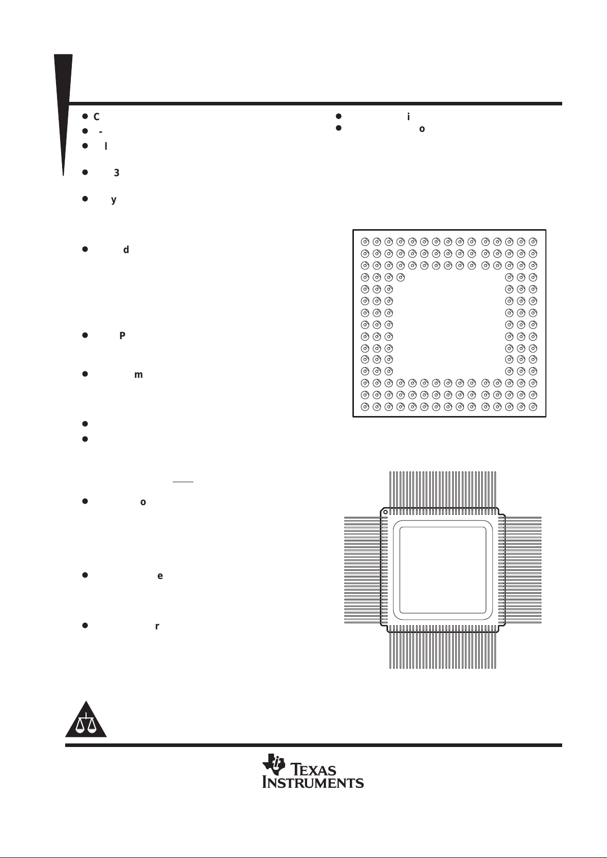
Packaging Options
– 145-Pin Grid Array Ceramic Package
(GB Suffix)
– 132-Pin Ceramic Quad Flat Pack
(Unformed Lead) (HT Suffix)
145-PIN GRID ARRAY PACKAGE
(BOTTOM VIEW)
A
B
C
D
E
F
G
H
J
K
L
M
N
P
R
123456789101112131415
132-PIN QUAD FLATPACK
(TOP VIEW)
1
132
99
34
10066
33 67
PRODUCTION DATA information is current as of publication date.
Products conform to specifications per the terms of Texas Instruments
standard warranty. Production processing does not necessarily include
testing of all parameters.
Copyright 1995, Texas Instruments Incorporated
Please be aware that an important notice concerning availability, standard warranty, and use in critical applications of
Texas Instruments semiconductor products and disclaimers thereto appears at the end of this data sheet.

SMJ34020A
GRAPHICS SYSTEM PROCESSOR
SGUS011B – APRIL 1991 – REVISED AUGUST 1995
2
POST OFFICE BOX 1443 • HOUSTON, TEXAS 77251–1443
description
The SMJ34020A graphics system processor (GSP) is the second generation of an advanced high-performance
CMOS 32-bit microprocessor optimized for graphics display systems. With a built-in instruction cache, the ability
to simultaneously access memory and registers, and an instruction set designed to expedite raster graphics
operations, the SMJ34020A provides user-programmable control of the CRT interface as well as the memory
interface (both standard DRAM and multiport video RAM). The 4-gigabit (512-megabyte) physical address
space is addressable on bit boundaries using variable width data fields (1 to 32 bits). Additional graphics
addressing modes support 1-, 2-, 4-, 8-, 16- and 32-bit wide pixels.
architecture
The SMJ34020A is a CMOS 32-bit processor with hardware support for graphics operations such as pixel block
transfers (PIXBL TS) during raster operations and curve-drawing algorithms. Also included is a complete set of
general-purpose instructions with addressing modes tuned to support high-level languages. In addition to its
ability to address a large external memory range, the SMJ34020A contains 30 general-purpose 32-bit registers,
a hardware stack pointer, and a 512-byte instruction cache. On-chip functions include 64 programmable I/O
registers that control CRT timing, input / output control, and parameters required by some instructions. The
SMJ34020A directly interfaces to DRAMs and VRAMs and generates raster control signals. The SMJ34020A
can be configured to operate as a standalone processor, or it can be used as a graphics engine with a host
system. The host interface provides a generalized communication port for any standard host processor. The
SMJ34020A also accommodates a multiprocessing or direct memory access (DMA) environment through the
request /grant interface protocols. Virtual memory systems are supported through bus-fault detection and
instruction continuation.
The SMJ34020A provides single-cycle execution of general-purpose instructions and most common integer
arithmetic and Boolean operations from its instruction cache. Additionally, the SMJ34020A incorporates a
hardware barrel shifter that provides a single-state bidirectional shift-and-rotate function for 1 to 32 bits.
The local-memory controller is designed to optimize memory access operations. It also supports pipeline
memory write operations of variable-sized fields and allows memory access and instruction execution in
parallel.
The SMJ34020A graphics-processing hardware supports pixel and pixel-array processing capabilities for both
monochrome and color systems at a variety of pixel sizes. The hardware incorporates two-operand and
three-operand raster operations with Boolean and arithmetic operations, XY addressing, window clipping,
window-checking operations, 1 to
n
bits-per-pixel transforms, transparency, and plane masking. The
architecture further supports operations on single pixel transfer (PIXT) instructions or on two-dimensional
arrays of arbitrary size (PIXBLTS).
The SMJ34020A ’ s flexible graphics-processing capabilities allow software-based graphics algorithms without
sacrificing performance. These algorithms include clipping to arbitrary window size, custom incremental-curve
drawing, two-operand raster operations, and masked two-operand raster operations.
The SMJ34020A provides for extensions to the basic architecture through the coprocessor interface. Special
instructions and cycle timings are included to enhance data flow to coprocessors without requiring the
coprocessor to decode the instruction stream, generate system addresses, or move data for the coprocessor
through the SMJ34020A.
SMJ34020A
GRAPHICS SYSTEM PROCESSOR
SGUS011B – APRIL 1991 – REVISED AUGUST 1995
3
POST OFFICE BOX 1443 • HOUSTON, TEXAS 77251–1443
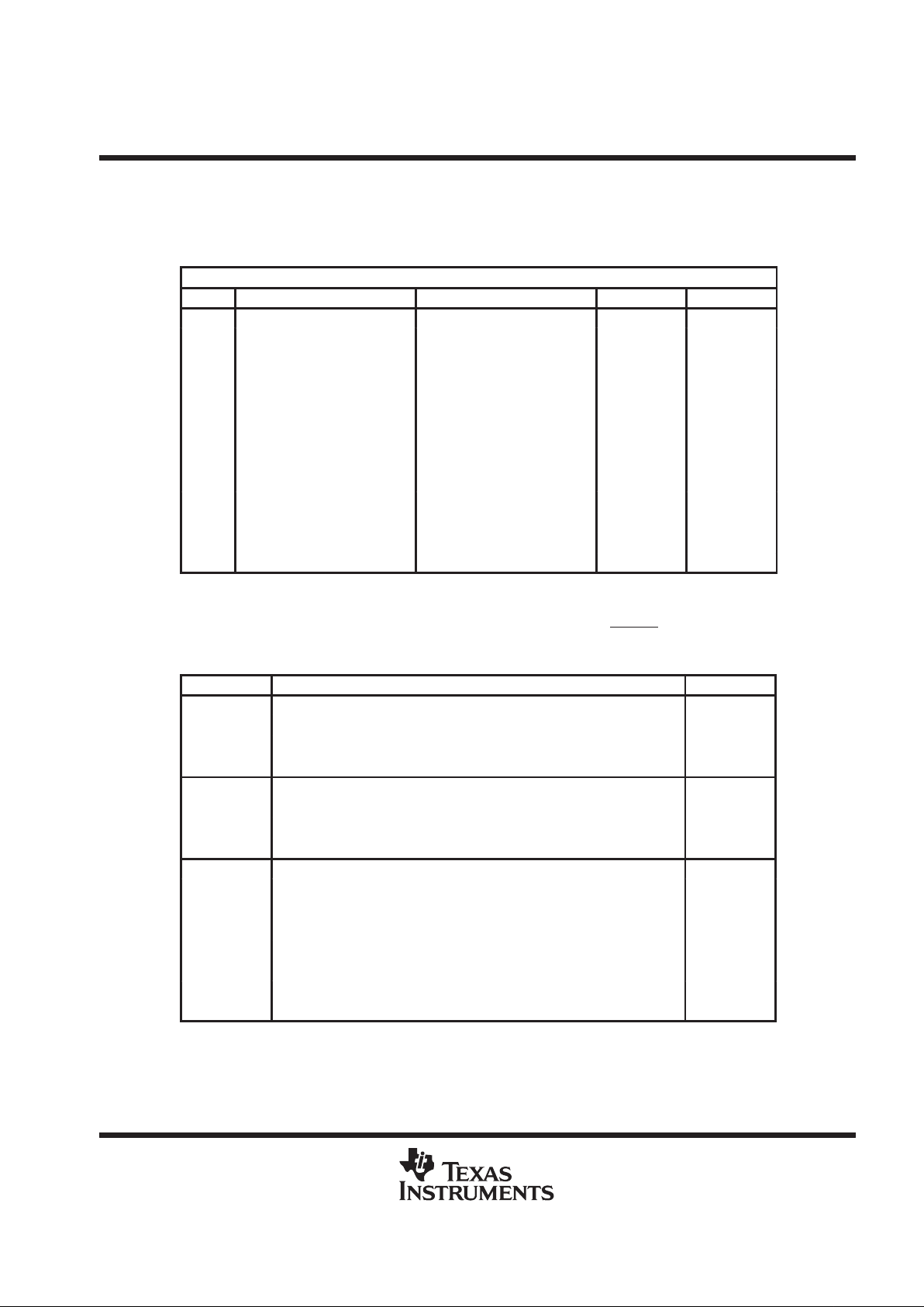
Pin Assignments – 145-Pin Grid Array Package
PIN PIN PIN PIN
NUMBER NAME NUMBER NAME NUMBER NAME NUMBER NAME
A1 V
SS
C9 RCA8 J1 EMU0 N15 LAD17
A2 ALTCH C10 RCA12 J2 GI P1 V
CC
A3 CBLNK/VBLNK C11 LAD30 J3 EMU1 P2 HWRITE
A4 HSYNC C12 V
SS
J13 LAD4 P3 HCS
A5 TR/QE C13 V
SS
J14 V
CC
P4 HA30
A6 RCA2 C14 V
CC
J15 LAD5 P5 HA27
A7 RCA3 C15 LAD26 K1 EMU2 P6 HA24
A8 V
CC
D1 RAS K2 RESET P7 HA22
A9 RCA6 D2 CAS2 K3 LINT2 P8 HA18
A10 RCA7 D3 V
SS
K13 V
SS
P9 HA14
A11 RCA10 D4
†
NU
†
K14 LAD3 P10 HA13
A12 SCLK D13 LAD28 K15 LAD20 P11 HA10
A13 LAD15 D14 LAD11 L1 LINT1 P12 HA7
A14 LAD29 D15 LAD10 L2 CAMD P13 HA5
A15 V
SS
E1 R1 L3 LRDY P14 HBS0
B1 CAS3 E2 V
CC
L13 LAD1 P15 LAD0
B2 WE E3 CAS1 L14 LAD2 R1 HREAD
B3 V
SS
E13 LAD27 L15 LAD19 R2 HA31
B4 CSYNC/HBLNK E14 LAD25 M1 BUSFLT R3 HA28
B5 VSYNC E15 LAD9 M2 PGMD R4 HA26
B6 RCA0 F1 HRDY M3 VCLK R5 HA23
B7 RCA1 F2 R0 M13 V
SS
R6 HA20
B8 RCA5 F3 V
SS
M14 LAD16 R7 HA19
B9 RCA9 F13 LAD24 M15 LAD18 R8 HA17
B10 RCA11 F14 LAD8 N1 SIZE16 R9 HA16
B11 LAD31 F15 V
SS
N2 V
CC
R10 HA15
B12 LAD14 G1 HINT N3 CLKIN R11 HA11
B13 V
CC
G2 HOE N4 V
SS
R12 HA9
B14 LAD13 G3 HDST N5 HA29 R13 HA8
B15 LAD12 G13 LAD7 N6 HA25 R14 HBS3
C1 CAS0 G14 V
SS
N7 HA21 R15 V
SS
C2 V
CC
G15 LAD23 N8 V
SS
C3 DDOUT H1 LCLK1 N9 V
SS
C4 DDIN H2 EMU3 N10 HA12
C5 V
SS
H3 LCLK2 N11 HA6
C6 SF H13 LAD22 N12 HBS2
C7 RCA4 H14 LAD21 N13 HBS1
C8 V
SS
H15 LAD6 N14 V
CC
†
This pin is provided for device orientation purpose only. Make no external connection.

SMJ34020A
GRAPHICS SYSTEM PROCESSOR
SGUS011B – APRIL 1991 – REVISED AUGUST 1995
4
POST OFFICE BOX 1443 • HOUSTON, TEXAS 77251–1443
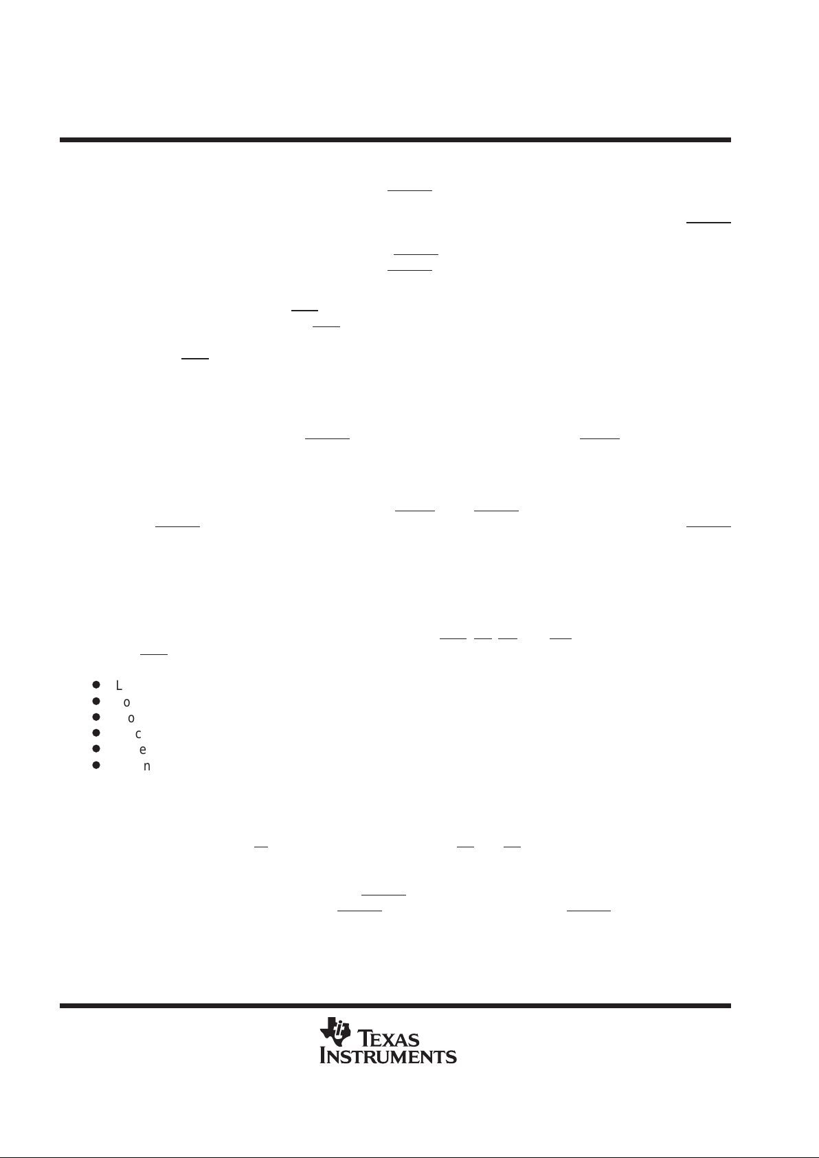
Pin Assignments – 132-Pin Ceramic Quad Flatpack Package
PIN PIN PIN PIN
NUMBER NAME NUMBER NAME NUMBER NAME NUMBER NAME
1 CAS3 34 HCS 67 LAD0 100 LAD29
2 CAS2 35 HA31 68 LAD16 101 LAD14
3 CAS1 36 HA30 69 LAD1 102 LAD30
4 CAS0 37 HA29 70 LAD17 103 LAD15
5 V
CC
38 HA28 71 LAD2 104 LAD31
6 RAS 39 HA27 72 LAD18 105 SCLK
7 V
SS
40 HA26 73 V
SS
106 RCA12
8 R0 41 HA25 74 LAD3 107 RCA11
9 R1 42 HA24 75 LAD19 108 RCA10
10 HOE 43 HA23 76 V
CC
109 RCA9
11 HDST 44 HA22 77 LAD4 110 RCA8
12 HRDY 45 HA21 78 LAD20 111 RCA7
13 HINT 46 HA20 79 LAD5 112 RCA6
14 EMU3 47 HA19 80 LAD21 113 RCA5
15 LCLK1 48 HA18 81 LAD6 114 V
CC
16 LCLK2 49 HA17 82 LAD22 115 V
SS
17 EMU1 50 V
SS
83 LAD7 116 RCA4
18 EMU0 51 HA16 84 LAD23 117 RCA3
19 EMU2 52 HA15 85 V
SS
118 RCA2
20 GI 53 HA14 86 V
SS
119 RCA1
21 RESET 54 HA13 87 LAD8 120 RCA0
22 LINT2 55 HA12 88 LAD24 121 SF
23 LINT1 56 HA11 89 LAD9 122 TR/QE
24 CAMD 57 HA10 90 LAD25 123 VSYNC
25 BUSFLT 58 HA9 91 LAD10 124 HSYNC
26 SIZE16 59 HA8 92 LAD26 125 CBLNK /VBLNK
27 PGMD 60 HA7 93 LAD11 126 CSYNC/HBLNK
28 LRDY 61 HA6 94 LAD27 127 V
SS
29 V
CC
62 HA5 95 V
CC
128 V
SS
30 VCLK 63 HBS3 96 LAD12 129 ALTCH
31 CLKIN 64 HBS2 97 LAD28 130 DDIN
32 HWRITE 65 HBS1 98 V
SS
131 DDOUT
33 HREAD 66 HBS0 99 LAD13 132 WE

SMJ34020A
GRAPHICS SYSTEM PROCESSOR
SGUS011B – APRIL 1991 – REVISED AUGUST 1995
5
POST OFFICE BOX 1443 • HOUSTON, TEXAS 77251–1443
Pin Functions
PIN
NAME I/O
†
DESCRIPTION
LOCAL MEMORY INTERF ACE
ALTCH O
Address latch. The high-to-low transitions of ALTCH can be used to capture the address and status available on LAD.
A transparent latch (such as a 54ALS373) maintains the current address and status as long as ALTCH
remains low.
BUSFLT I
Bus fault. External logic asserts BUSFLT high to the SMJ34020A to indicate that an error or fault has occurred on the
current bus cycle. BUSFLT is also used with LRDY to generate externally requested bus cycle retries so that the entire
memory address is presented again on LAD.
In the emulation mode, BUSFL T is used for write protecting mapped memory (by disabling CAS
outputs for the current
cycle).
DDIN O
Data bus direction in enable. DDIN is used to drive the active-high output enables on bidirectional transceivers (such
as the 54ALS623). The transceivers buffer data input and output on LAD0–LAD31 when the SMJ34020A is interfaced
to several memories.
DDOUT O
Data bus direction output enable. DDOUT drives the active-low output enables on bidirectional transceivers (such as
the 54ALS623). The transceivers buffer data input and output on LAD0–LAD31.
LAD0–LAD31 I/O
32-bit multiplexed local address/data bus. At the beginning of a memory cycle, the word address is output on
LAD4–LAD31 and the cycle status is output on LAD0–LAD3. After the address is presented, LAD0–LAD31 are used
for transferring data within the SMJ34020A system. LAD0 is the LSB and LAD31 is the MSB.
LRDY I
Local ready. External circuitry drives LRDY low to inhibit the SMJ34020A from completing a local-memory cycle it has
initiated. While LRDY remains low, the SMJ34020A waits unless the SMJ34020A loses bus priority or is given an
external RETRY request (through BUSFL T). Wait states are generated in increments of one full LCLK1 cycle. LRDY can
be driven low to extend local memory-read and memory-write cycles, VRAM serial-data-register-transfer cycles, and
DRAM-refresh cycles. During internal cycles, the SMJ34020A ignores LRDY.
PGMD I
Page mode. The memory-decode logic asserts PGMD low if the currently addressed memory supports burst (page
mode) accesses. Burst accesses occur as a series of CAS
cycles for a single RAS cycle to memory. LRDY is used with
BUSFLT to describe the cycle termination status for a memory cycle.
PGMD
is also used in emulation mode for mapping memory.
SIZE16 I
Bus size. The memory-decode logic can pull SIZE16 low if the currently addressed memory or port supports only 16-bit
transfers. SIZE16
can also be used to determine which 16 bits of the data bus are used for a data transfer.
In the emulation mode, SIZE16
is used to select the size of mapped memory.
DRAM AND VRAM CONTROL
CAMD I
Column-address mode. CAMD dynamically shifts the column address on the RCA0–RCA12 bus to allow the mixing
of DRAM and VRAM address matrices using the same multiplexed address RCA0–RCA12 signals.
CAS0–CAS3 O
Four column-address strobes. CAS outputs drive the CAS inputs of DRAMs and VRAMs. CAS0 –CAS3 strobe the
column address on RCA0–RCA12 to the memory. The four CAS
strobes provide byte write-access to the memory.
RAS O
Row-address strobe. RAS output drives the RAS inputs of DRAMs and VRAMs. RAS strobes the row address on
RCA0–RCA12 to memory.
RCA0–RCA12 O
Thirteen multiplexed row-address/column-address signals. At the beginning of a memory-access cycle, the row address
for DRAMs is present on RCA0–RCA12. The row address contains the most significant address bits for the memory.
As the cycle progresses, the memory column address is placed on RCA0–RCA12. The addresses that are actually
output during row and column times depend on the memory configuration (set by RCM0 and RCM1 in the CONFIG
register) and the state of CAMD during the access. RCA0 is the LSB, and RCA12 is the MSB.
SF O
Special function pin. SF is the special-function signal to 1M VRAMs that allows the use of block write, load write mask,
load color mask, and write using write mask. SF is also used to differentiate instructions and addresses for the
coprocessor as part of the coprocessor interface.
TR/QE O
Transfer/output-enable. TR/QE drives the TR/QE input of VRAMs. During a local memory-read cycle, TR/QE functions
as an active-low output enable to gate from memory to LAD0–LAD31. During special VRAM function cycles, TR
/QE
controls the type of cycle that is performed.
†
I = input, O = output
SMJ34020A
GRAPHICS SYSTEM PROCESSOR
SGUS011B – APRIL 1991 – REVISED AUGUST 1995
6
POST OFFICE BOX 1443 • HOUSTON, TEXAS 77251–1443
Pin Functions (Continued)
PIN
NAME I/O
†
DESCRIPTION
DRAM AND VRAM CONTROL (CONTINUED)
WE O Write enable. The active low WE drives the WE inputs of DRAMs and VRAMs. WE can also be used as the active
low write enable to static memories and other devices connected to the SMJ34020A local interface. During a
local-memory read cycle, WE
remains inactive high while CAS is strobed active low. During a local-memory write
cycle, WE
is strobed active low before CAS. During VRAM serial-data-register transfer cycles, the state of WE at
the falling edge of RAS
controls the direction of the transfer.
HOST INTERFACE
HA5–HA31 I Twenty-seven host address input signals. A host can access a long word by placing the address on these lines.
HA5–HA31 correspond to LAD5–LAD31 that output the address to the local memory.
HBS0–HBS3 I Four host byte selects. HBS0 –HBS3 identify which bytes within the long word are being selected.
HCS I Host chip select. A host drives HCS low to latch the current host address present on HA5–HA31 and the host byte
selects on HBS0–HBS3. HCS
also enables host access cycles to the SMJ34020A I/O registers or local memory.
During the low-to-high transition of RESET
, the level on HCS determines whether the SMJ34020A is halted (HCS
is high for host-present mode) or whether it begins executing its reset service routine (HCS is low for self-bootstrap
mode).
HDST O Host data-latch strobe. The rising edge of HDST latches data from the SMJ34020A local address space to the
external host data latch on host read accesses. HDST can be used in conjunction with HRDY to indicate that data
is valid in the external data latch.
HINT O Host Interrupt. HINT allows the SMJ34020A to interrupt a host by setting the INTOUT bit in the HSTCTLL I/O register.
HINT
can also be used to interrupt the host if a BUSFLT or RETRY occurs due to a host access cycle.
HOE O Host data latch output enable. HOE enables data from host data latches to the SMJ34020A local address space on
host write cycles. HOE
can be used in conjunction with HRDY to indicate data has been written to memory from the
external data latch.
HRDY O Host ready. HRDY is normally low and goes high to indicate that the SMJ34020A is ready to complete a host-initiated
read or write cycle. If the SMJ34020A is ready to accept the access request, HRDY is driven high and the host can
proceed with the access. A host can use HRDY logically combined with HDST and HOE
to determine when the local
bus access cycles have completed.
HREAD I Host read strobe. HREAD is driven low during a read request from a host processor. This notifies the SMJ34020A
that the host is requesting access to the I/O registers or to local memory. HREAD
should not be asserted at the same
time that HWRITE
is asserted.
HWRITE I Host write strobe. HWRITE is driven low to indicate a write request by a host processor . This notifies the SMJ34020A
that a write request is pending. The rising edge of HWRITE
is used to indicate that the host has latched data to be
written in the external data transceivers. HWRITE
should not be asserted at the same time HREAD is asserted.
SYSTEM CONTROL
CLKIN I Clock input. CLKIN generates LCLK1 and LCLK2, to which all processor functions in the SMJ34020A are
synchronous. A separate asynchronous input clock (VCLK) controls the video timing and video registers.
LCLK1, LCLK2 O Local output clocks. LCLK1 and LCLK2 are 90 degrees out of phase with each other. They provide convenient
synchronous control of external circuitry to the internal timing. All signals output from the SMJ34020A (except the
CRT timing signals) are synchronous to LCLK1 and LCLK2.
LINT1, LINT2 I Local interrupt requests. Interrupts from external devices are transmitted to the SMJ34020A on LINT1 and LINT2.
Each local interrupt signal activates the request for one of two interrupt request levels. An external device generates
an interrupt request by driving the appropriate interrupt request pin to its active-low state. LINT1
, LINT2 should
remain low until the SMJ34020A recognizes it. LINT1
, LINT2 can be applied asynchronously to the SMJ34020A as
they are synchronized internally before use.
RESET I System reset. During normal operation, RESET is driven low to reset the SMJ34020A. When RESET is asserted
low, the SMJ34020A ’s internal registers are set to an initial known state and all output and bidirectional pins are driven
either to inactive levels or to the high-impedance state. The SMJ34020A’ s behavior following reset depends on the
level of the HCS
input just before the low-to-high transition of RESET . If HCS is low, the SMJ34020A begins executing
the instructions pointed to by the reset vector. If HCS
is high, the SMJ34020A is halted until a host processor writes
a 0 to the HLT bit in the HSTCTLL register.
†
I = input, O = output
SMJ34020A
GRAPHICS SYSTEM PROCESSOR
SGUS011B – APRIL 1991 – REVISED AUGUST 1995
7
POST OFFICE BOX 1443 • HOUSTON, TEXAS 77251–1443
Pin Functions (Continued)
PIN
NAME I/O
†
DESCRIPTION
POWER
V
CC
‡
I Nominal 5-V power supply inputs. Five pins on QFP; Nine pins on PGA.
V
SS
‡
I Electrical ground inputs. Nine pins on QFP; 17 pins on PGA.
EMULATION CONTROL
EMU0–EMU2 I Emulation pins 0–2
EMU3 O Emulation pin 3
MULTIPROCESSOR INTERFACE
GI I Bus grant input. External bus arbitration logic drives GI low to enable the SMJ34020A to gain access to the
local-memory bus. The SMJ34020A must release the bus if GI
is high so that another device can access the bus.
R1, R0 O Bus request and control. R1 and R0 indicate a request for use of the bus in a multiprocessor system; they are
decoded as shown below:
R1 R0 Bus Request Type
L L High-priority bus request
L H Bus-cycle termination
H L Low-priority bus request
H H No bus request pending
A high-priority bus request provides for VRAM serial-data-register transfer cycles (midline or blanked), DRAM
refresh (when 12 or more refresh cycles are pending), or a host-initiated access. The external arbitration logic
should grant the request as soon as possible by asserting GI
low.
A low-priority bus request is used to provide for CPU-requested access and DRAM refresh (when less than
12 refresh cycles are pending).
Bus-cycle termination status is provided so that the arbitration logic can determine that the device currently
accessing the bus is completing an access, and other devices can compete for the next bus cycle. A
no-bus-request-pending status is output when the currently active device does not require the bus on subsequent
cycles.
VIDEO INTERFACE
CBLNK / VBLNK O Composite blanking/vertical blanking. CBLNK / VBLNK can be programmed to select one of two blanking
functions:
Composite blanking for blanking the display during both horizontal and vertical retrace periods in
composite-sync-video mode
Vertical blanking for blanking the display during vertical retrace in separate-sync-video mode.
Immediately following reset, CBLNK
/ VBLNK is configured as a CBLNK output.
CSYNC / HBLNK I/O Composite sync/horizontal blanking. CSYNC / HBLNK can be programmed to select one of two functions:
Composite sync (either input or output as set by a control bit in the DPYCTL register) in
composite-sync-video mode:
As an input, extracts HSYNC
and VSYNC from externally generated horizontal sync pulses
As an output,
CSYNC / HBLNK generates active-low composite-sync pulses from either externally
generated HSYNC
and VSYNC signals or signals generated by the SMJ34020A’ s on-chip video timers
Horizontal blank (output only) for blanking the display during horizontal retrace in separate-sync-video mode.
Immediately following reset, CSYNC
/ HBLNK is configured as a CSYNC input.
HSYNC I/O Horizontal sync. HSYNC is the horizontal sync signal that controls external video circuitry. HSYNC can be
programmed to be either an input or an output by modifying a control bit in the DPYCTL register.
As an output, HSYNC
is the active-low horizontal-sync signal generated by the SMJ34020A’s on-chip video
timers.
As an input, HSYNC
synchronizes the SMJ34020A video-control registers to externally generated
horizontal-sync pulses. The actual synchronization can be programmed to begin at any VCLK cycle; this
allows for any external pipelining of signals.
Immediately following reset, HSYNC
is configured as an input.
†
I = input, O = output
‡
For proper SMJ34020A operation, all VCC and VSS pins must be connected externally.
SMJ34020A
GRAPHICS SYSTEM PROCESSOR
SGUS011B – APRIL 1991 – REVISED AUGUST 1995
8
POST OFFICE BOX 1443 • HOUSTON, TEXAS 77251–1443
Pin Functions (Continued)
PIN
NAME I/O
†
DESCRIPTION
VIDEO INTERFACE (CONTINUED)
SCLK I Serial data clock. SCLK is the same as the signal that drives VRAM serial data registers. SCLK allows the SMJ34020A
to track the VRAM serial-data-register count, providing serial-register transfer and midline-reload cycles. (SCLK can
be asynchronous to VCLK; however, it typically has a frequency that is a multiple of the VCLK frequency).
VCLK I Video clock. VCLK is derived from a multiple of the video system’s dot clock and is used internally to drive the video
timing logic.
VSYNC I/O Vertical sync. VSYNC is the vertical sync signal that controls external video circuitry . VSYNC can be programmed to
be either an input or an output by modifying a control bit in the DPYCTL register.
As an output, VSYNC
is the active-low vertical-sync signal generated by the SMJ34020A’ s on-chip video timers.
As an input, VSYNC
synchronizes the SMJ34020A video-control registers to externally generated vertical-sync
pulses. The actual synchronization can be programmed to begin at any horizontal line; this allows for any
external pipelining of signals.
Immediately following reset, VSYNC
is configured as an input.
†
I = input, O = output
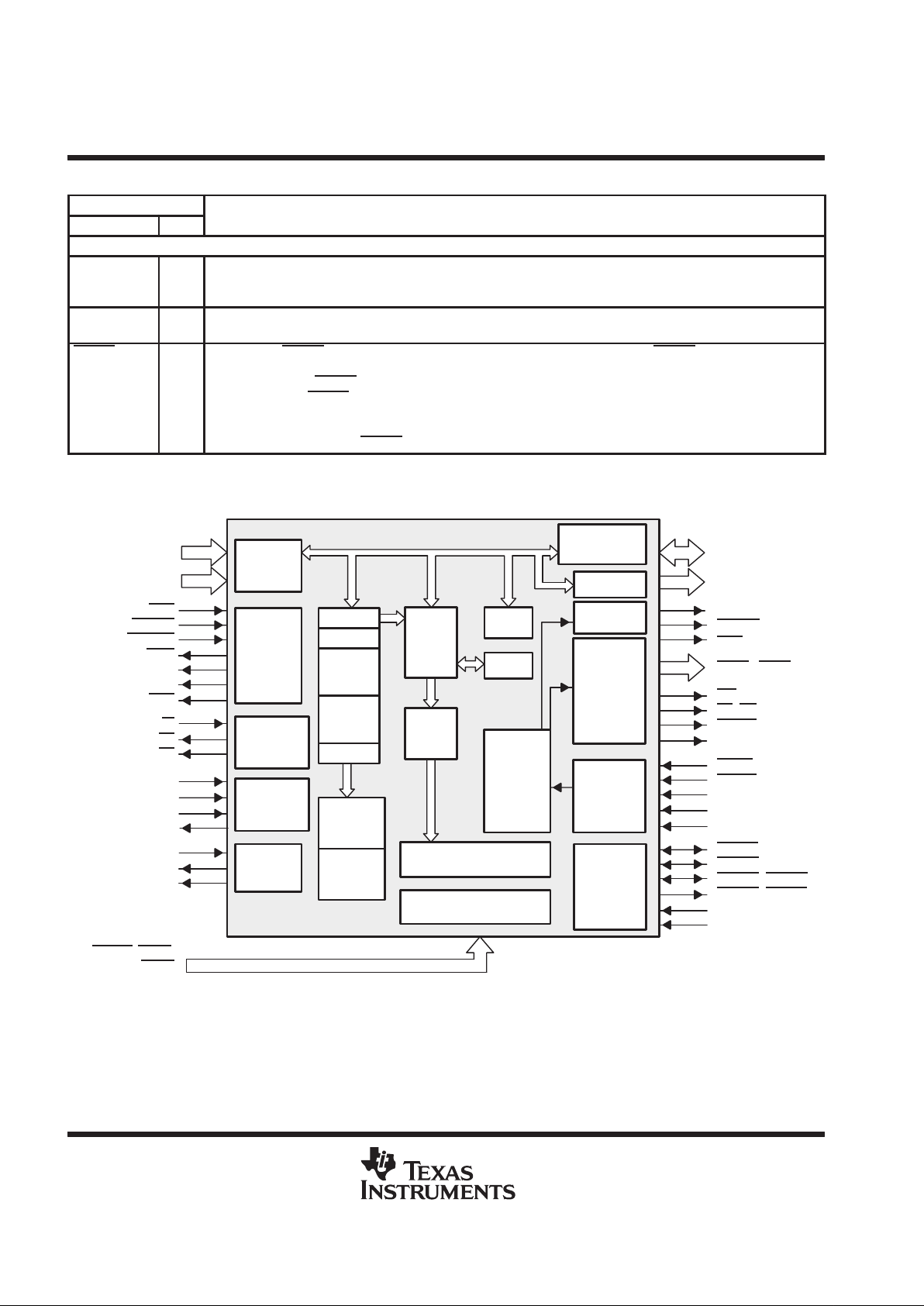
functional block diagram
Register
HA5–HA31
HBS0–HBS3
HCS
HREAD
HWRITE
HINT
HRDY
HDST
HOE
GI
R0
R1
EMU0
EMU1
EMU2
EMU3
CLKIN
LCLK1
LCLK2
RESET
, LINT1,
LINT2
LAD0–LAD31
RCA0–RCA12
DDIN
DDOUT
RAS
CAS0–CAS3
WE
TR/QE
ALTCH
SF
PGMD
SIZE16
LRDY
BUSFLT
CAMD
VSYNC
HSYNC
CSYNC/HBLNK
CBLNK/VBLNK
VCLK
SCLK
27
4
32
13
Host
Address
Latch
Host
Interface
Multi-
Processor
Interface
Emulation
Interface
System
Clocks
Buffer/
MUX
Bus
DRAM/
VRAM
Interface
Bus
Interface
Video
Timing
and
Control
Local
Memory
and
Bus
Timing
I/O
LRU
Regs
ALU
Barrel
Shifter
Microcontrol ROM
Reset and Interrupts
Control
Page-mode
Register
Cache
PC
ST
SP
Decode
4
Register
File A
Register
File B

SMJ34020A
GRAPHICS SYSTEM PROCESSOR
SGUS011B – APRIL 1991 – REVISED AUGUST 1995
9
POST OFFICE BOX 1443 • HOUSTON, TEXAS 77251–1443
architecture (continued)
register files
Boolean, arithmetic, pixel-processing, byte, and field-move instructions operate on data within the
general-purpose register files. The SMJ34020A contains two register files of fifteen 32-bit registers and a
system stack pointer (SP). The SP is addressed in both register file A and register file B as a sixteenth register.
Transfers between registers and memory are facilitated using a complete set of field
move
instructions with
selectable field sizes.
The 15 general-purpose registers in register file A are used for high-level language support and
assembly-language programming. The 15 registers in register file B are dedicated to special functions during
PIXBLTS and other pixel operations but can be used as general-purpose registers at other times.
stack pointer (SP)
The stack pointer is a dedicated 32-bit internal register that points to the top of the system stack.
program counter (PC)
The SMJ34020A’s 32-bit program counter register points to the next instruction-stream word to be fetched.
Since instruction words are aligned to 16-bit boundaries, the four LSBs of the PC are always zero.
instruction cache
An on-chip cache contains 512 bytes of RAM and provides unimpeded access to instructions. The cache
operates automatically and is transparent to software. The cache is divided into four 128-byte segments.
Associated with each segment is a 22-bit segment start address register (SSA) to identify the addresses in
memory corresponding to the current contents of the cache segment. Each cache segment is further partitioned
into eight subsegments of four long words (32 bits) each. Each subsegment has an associated present (P) flag
to indicate whether or not the subsegment contains valid data.
The cache is loaded only when an instruction requested by the execution section of the SMJ34020A is not
already contained within the cache. A least-recently-used (LRU) algorithm determines which of the four
segments of the cache is overwritten with new data. For this purpose, an internal four-by-two LRU stack keeps
track of cache usage. Although the cache is loaded so as to always fill a subsegment completely , not all eight
subsegments within a segment are necessarily filled (this is dependent upon the instruction stream).
status register
The status register (ST) is a special purpose 32-bit register dedicated to status codes set by the results of implicit
and explicit compare operations and parameters used to specify the length and behavior of fields 0 and 1. During
an interrupt, when the IX bit in the ST is placed on the stack, it indicates that execution of an interruptable
instruction (PIXBLT, FILL or LINE) was halted to service the interrupt. The single-step bit causes a trap to the
single-step vector (located at address FFFF FBE0h) after the execution of one instruction when the bit is set
high. Normal program execution occurs when the bit is set low.
fields, bytes, words, long words, pixels and pixel arrays
The SMJ34020A outputs a 28-bit address on LAD4–LAD31 that is valid at the falling edge of ALTCH
. The most
significant 27 bits (LAD5–LAD31) define a 32-bit-long word of physical memory; logically, however, the
SMJ34020A views memory data as fields addressable at the bit level. The least significant bit of the 28-bit
address (LAD4) is used to select the odd or even word when accessing 16-bit memories (indicated by SIZE16
asserted low). Primitive data types supported by the SMJ34020A include bytes, words, long words, pixels, two
independent fields of from 1 to 32 bits, and user-defined pixel arrays.
Words and long words, respectively, refer to 16- and 32-bit values that are aligned on 32-bit boundaries.
SMJ34020A
GRAPHICS SYSTEM PROCESSOR
SGUS011B – APRIL 1991 – REVISED AUGUST 1995
10
POST OFFICE BOX 1443 • HOUSTON, TEXAS 77251–1443
fields, bytes, words, long words, pixels and pixel arrays (continued)
The two independent fields are referenced as field 0 and field 1. The attributes of these fields (field size and sign
extension within a register) are defined in the status register as FS0, FE0, FS1, and FE1. Fields 0 and 1 are
specified independently to be signed or unsigned and from 1 to 32 bits in length. Bytes are special 8-bit cases
of the field data type, while pixels are 1, 2, 4, 8, 16, or 32 bits in length. In general, fields (including bytes) can
start and terminate on arbitrary bit boundaries; however, pixels must pack evenly into 32-bit-long words.
pixel operations
Pixel arrays are two-dimensional data types of user-defined width, length, pixel depth (number of bits per pixel),
and pitch (distance between rows). A pixel or pixel array can be accessed by means of either its memory address
or its XY coordinates. Transfers of individual pixels or pixel blocks are influenced by the pixel processing,
transparency , window checking, plane masking, pixel masking, or corner adjustment operations selected. For
further information, see the
TMS32020 User’s Guide
, literature number SPVU019.
transparency
Transparency is a mechanism that allows the surrounding pixels in an array to be specified as invisible. This
is useful for ensuring that only the object and not the rectangle surrounding it are written to the display. The
SMJ34020A provides four transparency modes:
D
No transparency
D
Transparency on result equal zero
D
Transparency on source equal COLOR0
D
Transparency on destination equal COLOR0
D
Refer to the
TMS34020 User’s Guide
for more information.
I/O registers
The SMJ34020A contains an on-chip block of sixty-four 16-bit locations (mapped into the SMJ34020A’s
memory address space) that are used for I/O control registers. Eight of these are used by the host interface logic
and are not available to the user. Forty-seven I/O registers control parameters necessary to configure the
operation and report status of the following interfaces:
D
Host interface
D
Local memory
D
Video timing
D
Screen refresh
D
External interrupts
D
Internal interrupts
host interface registers
The host interface registers (HSTDATA, HSTADRL, HSTADRH, HSTCTLL, and HSTCTLH) are provided to
facilitate communications between the SMJ34020A and a host processor and maintain compatibility with the
SMJ34010. The registers are mapped into five of the I/O locations accessible to the SMJ34020A.
Two of these registers (HSTCTLL and HSTCTLH) are used to provide control by the host. This control consists
of the passing of interrupt requests, flushing the instruction cache, halting the SMJ34020A, transmitting a
non-maskable interrupt request to the SMJ34020A, enabling emulation interrupts, and setting host access
modes and configurations.
The other three registers are simple read/write registers to allow the SMJ34020A software to leave addresses
for the host at a known location and allow compatibility with some SMJ34010 software.
SMJ34020A
GRAPHICS SYSTEM PROCESSOR
SGUS011B – APRIL 1991 – REVISED AUGUST 1995
11
POST OFFICE BOX 1443 • HOUSTON, TEXAS 77251–1443
memory interface control registers
Some of the I/O registers are used to control various local memory interface functions, including:
D
Frequency of DRAM refresh cycles
D
Masking (read/write protection) of individual color planes
D
DRAM row/column addressing configuration
D
Accessing mode (big endian/little endian)
D
Bus fault and retry recovery
video timing and screen refresh
Twenty-eight I/O registers are dedicated to video timing and screen refresh functions. The SMJ34020A can be
configured to drive composite sync or separate sync displays.
In composite sync mode, the SMJ34020A can be set to extract VSYNC
and HSYNC from an external CSYNC
or it can be used to generate CSYNC from separate VSYNC and HSYNC inputs. Internally, the SMJ34020A
can be set to preset the horizontal and vertical counts on receipt of an external sync signal. This allows
compensation for any combination of internal and external delays that occur in the video synchronization
process. The HCOUNT register is loaded from SETHCNT by an external HSYNC
, VCOUNT is loaded from
SETVCNT on an external VSYNC
, and an external CSYNC loads both HCOUNT and VCOUNT from SETHCNT
and SETVCNT, respectively.
The SMJ34020A directly supports VRAMs by generating the serial-data-register transfer cycles necessary to
refresh the display . The memory locations from which the display information is taken, as well as the number
of horizontal scan lines displayed between serial-data-register transfer cycles, are programmable.
The SMJ34020A supports various display resolutions and either interlaced or noninterlaced video. The
SMJ34020A can optionally be programmed to synchronize to externally generated sync signals so that images
created by the SMJ34020A can be superimposed upon images created externally . The external sync mode can
also be used to synchronize the video signals generated by two or more SMJ34020As in a multiple-SMJ34020A
graphics system.
CPU control registers
Five of the I/O registers (CONVDP, CONVMP, CONVSP, CONTROL, and PSIZE) provide CPU control to
configure the SMJ34020A for operation with specific characteristics. These characteristics include pitches for
pixel transfers, window checking mode, Boolean or arithmetic pixel processing operation, transparency mode,
PIXBLT direction control, and pixel size.
interrupt interface registers
Two dedicated I/O registers (INTENB and INTPEND) monitor and mask interrupt requests to the SMJ34020A,
including two externally generated interrupts and three internally generated interrupts. An internal interrupt
request can be generated on one of the following conditions.
D
Window violation: an attempt has been made to write a pixel to a location inside or outside a specified
window boundary.
D
Host interrupt: the host processor has set the interrupt request bit in the host control register.
D
Display interrupt: a specified horizontal line in the frame has been displayed on the screen.
D
Bus fault
D
Single-step emulator
A nonmaskable interrupt occurs when the host processor sets a control bit in the host interface register (NMI
in HSTCTLH). The host-initiated interrupt is associated with a mode bit (NMIM in HSTCTLH) that enables and
disables saving of the processor state on the stack when the interrupt occurs. This is useful if the host wishes
to use the host interrupt before releasing the SMJ34020A to execute instructions (that is, before the stack
pointer is initialized). A dedicated terminal controls the SMJ34020A reset function.

SMJ34020A
GRAPHICS SYSTEM PROCESSOR
SGUS011B – APRIL 1991 – REVISED AUGUST 1995
12
POST OFFICE BOX 1443 • HOUSTON, TEXAS 77251–1443
memory controller/local-memory interface
The memory controller manages the SMJ34020A’s interface to the local memory and automatically performs
the bit alignment and masking necessary to access data located at arbitrary bit boundaries within memory . The
memory controller operates autonomously with respect to the CPU. It has a write queue one field (1 to 32 bits)
deep that permits it to complete those memory cycles necessary to insert a field into memory without delaying
the execution of subsequent instructions. Only when a second memory operation is required before completion
of the first operation is the SMJ34020A forced to defer execution of the subsequent instruction.
The SMJ34020A directly interfaces to standard DRAMs and in particular, to standard video RAMs (VRAMs)
such as the SMJ44C25x multiport VRAMs. The SMJ34020A memory interface consists of the local
address/data bus (LAD), the DRAM row/column address (RCA) bus, and associated control signals. The
currently selected word address (28 bits) and status (4 bits) are multiplexed with data on LAD. The RCA bus
allows direct connection to address/address multiplexed DRAMs from 64K to 16M. Refresh for DRAMs is
supported by CAS
-before-RAS (CBR) refresh cycles.
BIT 232 –1
(Last Bit in Memory)
68 Words
226 –66560 Words
(67 042 304 Words)
(3 × 226) –64K
(201 261 056 Words)
444 Words
65024 Words
512 Words
448 Words
64 Words
64K Words
Interrupt Vectors and
Extended Trap V ectors
Reserved for Interrupt Vectors
and Extended Trap Vectors
General Use and
Extended Trap V ectors
General Use and Extended
Trap Vectors
Bit 0
(First Bit in Memory)
General Use
Reserved for System I/O
Reserved for I/O Registers
I/O Registers
General Use
ADDRESS
FFFFFFF0h
FFFFFBC0h
FFFFFBB0h
FFFFE000h
FFFFDFF0h
FFFF0000h
FFEFFFF0h
C0004000h
C0003FF0h
C0002000h
C0001FF0h
C0000400h
C00003F0h
C0000000h
BFFFFFF0h
00100000h
000FFFF0h
00000000h
16
Figure 1. Memory Map

SMJ34020A
GRAPHICS SYSTEM PROCESSOR
SGUS011B – APRIL 1991 – REVISED AUGUST 1995
13
POST OFFICE BOX 1443 • HOUSTON, TEXAS 77251–1443
reset
Reset puts the SMJ34020A into a known initial state. This state is entered when the input signal at RESET
is
asserted low. While RESET
remains asserted, all outputs are in a known state, no DRAM refresh cycles take
place, and no screen refresh cycles are performed.
The state of the HCS
input on the CLKIN cycle before the low-to-high transition of RESET determines whether
the SMJ34020A is halted or begins executing instructions. The SMJ34020A can be in one of two modes,
host-present or self-bootstrap mode.
Host-present mode: if HCS
is high at the end of reset, SMJ34020A instruction execution halts and remains
halted until the host clears the HL T (halt) bit in HSTCTLH (host control register). Following reset, the RAS
cycles
required to initialize the dynamic RAMs are performed automatically by the GSP memory control logic. The host
can request a memory access after the eight RAS
initialization cycles have completed. The SMJ34020A
automatically performs DRAM refresh cycles at regular intervals although the SMJ34020A remains halted until
the host clears the HLT bit. Only then does SMJ34020A fetch the level-0 vector address from location
FFFFFFE0h and begin executing the reset service routine.
Self-bootstrap mode: if HCS
is low at the end of reset, the SMJ34020A first performs eight refresh cycles to
initialize the DRAMs. Immediately following the eight refresh cycles, the GSP fetches the level-0 vector address
from location FFFFFFE0h and begins executing the reset service routine.
At the time the SMJ34020A fetches the level-0 vector address (the reset vector), the least significant four bits
(bit address part) are used to load configuration data that establishes the initial condition of the
big-endian/little-endian mode and the current RCA bus configuration bits in the CONFIG register as described
in the I/O register section.
Unlike other interrupts and software traps, reset does not save the previous ST or PC values (this can also occur
on host initiated nonmaskable interrupts if the NMIM bit in HSTCTLH is set to a 1) because the value of the stack
pointer just before a reset is generally not valid. Saving these values on the stack could contaminate valid
memory locations. A TRAP 0 instruction, which uses the same vector address as reset, similarly does not save
the ST or PC values.
asserting reset
A reset is initiated by asserting RESET to its active-low level. T o reset the SMJ34020A at powerup, RESET must
remain active low for a minimum of 40 local clock periods (LCLK1 and LCLK2) after power levels have become
stable. At times other than powerup, the SMJ34020A can be reset by holding RESET
low for a minimum of four
local clock periods; the GSP enters an internal reset state for 34 local clock cycles. While in the internal reset
state and RESET
is high, memory-refresh cycles occur.
reset and multiprocessor synchronization
The synchronization of multiple SMJ34020As sharing a local memory is done using the RESET input. In
systems where the multiprocessor interface is used to control the access to a common memory , the processors
must be synchronized. Synchronization is achieved by taking RESET
high within a specific interval relative to
CLKIN. This can be done by using CLKIN to clock the RESET
as received by the SMJ34020As. All SMJ34020As
to be synchronized should use the same CLKIN and RESET
inputs. All of the local memory and bus control
signals should be connected in parallel (without buffers) between the processors. After powerup, the
processors are not necessarily synchronized with respect to the particular quarter cycle in progress. The rising
edge of RESET
is used to set the SMJ34020A to a particular quarter cycle by adding Q1 cycles. All SMJ34020As
in a multiprocessor environment operate on the same quarter cycle within 10 quarter cycles after the rising edge
of RESET
.

SMJ34020A
GRAPHICS SYSTEM PROCESSOR
SGUS011B – APRIL 1991 – REVISED AUGUST 1995
14
POST OFFICE BOX 1443 • HOUSTON, TEXAS 77251–1443
reset and DRAM/VRAM initialization
The SMJ34020A drives its RAS signal inactive high as long as RESET remains low. The specifications for
certain DRAM and VRAM devices require that RAS
be driven inactive-high for 1 millisecond after power is stable
to provide the proper conditions for the DRAMs. Typically, eight RAS
cycles are also required to initialize the
DRAMs for proper operation. In general, holding RESET
low for t microseconds ensures that RAS remains high
initially for
t–(10tQ)
microseconds, tQ being the quarter-cycle time as defined by the input clock period, t
c(CHI)
.
The SMJ34020A memory controller automatically inserts the required eight RAS
cycles after all resets (after
powerup or after the internal reset state) by issuing CAS
-before-RAS refresh cycles before it allows the CPU
access to memory . A host must delay requests to memory until the initialization cycles have had sufficient time
to complete. Immediately following reset, the SMJ34020A is set to perform a refresh sequence every eight
cycles.
At times other than powerup, to maintain the memory in DRAMs and do a reset, the RESET
pulse must not
exceed the maximum refresh interval of the DRAMs minus the time for the SMJ34020A to refresh the memories.
On reset, the SMJ34020A is set to do a refresh cycle every eight local clock periods. A 30-MHz (CLKIN) system
with one (refresh) bank of D/VRAM would be completely refreshed in one sixteenth of the total memory refresh
interval. The reset pulse then should not exceed about fifteen-sixteenths of the total refresh interval required
by the DRAMs to maintain memory integrity.
If RESET
remains low longer than the maximum refresh interval specified for the memory , the previous contents
of the local memory can not be valid after the reset.
initial state following reset
While RESET is asserted low (or while in the internal reset state), the SMJ34020A’s output and bidirectional
pins are forced to the states below.
INITIAL STATE OF PINS FOLLOWING A RESET (WITH GI LOW)
†
OUTPUTS DRIVEN HIGH OUTPUTS DRIVEN LOW
BIDIRECTIONALS DRIVEN TO
HIGH IMPEDANCE
RAS HRDY VSYNC
CAS0–CAS3 CBLNK/VBLNK HSYNC
WE DDIN CSYNC/HBLNK
TR/QE LAD0–LAD31
DDOUT
ALTCH
HINT
R0
R1
HOE
HDST
EMU3
RCA0–RCA12
SF
†
If GI is high, then all GI-controlled pins are high-impedance. GI-controlled pins are RAS, CAS0–CAS3, WE, TR/QE, DDOUT, DDIN, ALTCH,
HOE
, HDST, RCA0–RCA12, LAD0–LAD31, and SF .
Immediately following reset, all I/O registers are cleared (set to 0000) with the exception of the HLT bit in the
HSTCTLH register. The HLT bit is set to 1 if HCS
is high just prior to the low-to-high transition of RESET;
otherwise, it is set to 0.
SMJ34020A
GRAPHICS SYSTEM PROCESSOR
SGUS011B – APRIL 1991 – REVISED AUGUST 1995
15
POST OFFICE BOX 1443 • HOUSTON, TEXAS 77251–1443
reset and DRAM/VRAM initialization (continued)
Just prior to the execution of the first instruction in the reset routine, the SMJ34020A’ s internal registers are in
the following states:
D
General-purpose register files A and B are uninitialized.
D
The ST is set to 0000 0010h.
D
The PC contains the most-significant 28 bits of the vector fetched from memory address FFFF FFE0h (the
least significant four bits of the PC are set to zero).
D
The BEN bit in the I/O register CONFIG is set to the least significant bit read from the vector fetched from
memory address FFFF FFE0h.
D
The CBP, RCM0, and RCM1 bits in the I/O register CONFIG are set to the corresponding bits read from
the vector fetched from memory address FFFF FFE0h. The configuration byte protect bit (CBP) can be set
high to prevent further modification of the lower eight bits of the I/O register CONFIG.
The state of the instruction cache at this time is as follows:
D
The SSA (segment start address) registers are uninitialized.
D
The LRU (least recently used) stack is set to the initial sequence 0, 1, 2, 3, where 0 occupies the most
recently used position and 3 occupies the least recently used position.
D
All P (present) flags are cleared to 0s.
local memory and DRAM/VRAM interface
The SMJ34020A local memory interface consists of an address/data multiplexed bus on which addresses and
data are transmitted. The associated control signals support memory widths of 16 or 32 bits, burst (page-mode)
accesses, local memory-wait states, and optional external data bus buffers. The SMJ34020A DRAM /VRAM
interface consists of an address/address multiplexed bus and the control signals to interface directly to both
DRAMs and VRAMs. The local memory interface and the DRAM/VRAM interface are interrelated and,
therefore, considered together for this description. At the beginning of a typical memory cycle, the address and
status of the current cycle are output on LAD while the ROW address is output on the row/column address (RCA)
bus. AL TCH
and RAS are used to latch the address/status and ROW address, respectively , on these two buses.
LAD is then used to transfer data to or from the memory while the RCA bus is set to the column address for the
memory. (NOTE: LAD31 is the most significant bit of the address or data).
W
31
543 0
Address
STS
LAD During the Address Cycle
Address — Memory address (select for 128M 32-bit long-words)
W = 0 — Access to lower 16-bit word (even-addressed word or 32-bit boundary)
W = 1 — Access to upper 16-bit word (odd-addressed word)
STS — Bus cycle status code

SMJ34020A
GRAPHICS SYSTEM PROCESSOR
SGUS011B – APRIL 1991 – REVISED AUGUST 1995
16
POST OFFICE BOX 1443 • HOUSTON, TEXAS 77251–1443
local memory and DRAM/VRAM interface (continued)
The address output on the row/column address (RCA) lines is determined by the row/column mode bits (RCM0
and RCM1 in the I/O registers CONFIG) and the state of column-address mode (CAMD) during each memory
cycle. The CAMD is sampled on the internal Q4 clock phase, which allows CAMD to be generated by static logic
wired to the local address/data (LAD) bus.
BASIC MEMORY ROW/COLUMN ACCESS MODES
RCM1 RCM VRAM
MODE
†
ADDRS‡BANKS
§
CAMD SUPPORT MATRICES
¶
0 0 64K × N 8 16 64K × 16, 64K × 32, 256K × 16, 256K × 32, 1M × 16, 1M × 32
0 1 256K × N 9 8 2564K × 16, 256K × 32, 1M × 16, 1M × 32, 4M × 32
1 0 1M × N 10 4 1M × 16, 1M × 32, 4M × 16, 4M × 32
1 1 4M × N 11 2 4M × 16, 4M × 32, 16M × 32
†
VRAM mode = basic size of VRAM addressing supported with CAMD = 0
‡
Addrs = number of RCA signals required to provide row/column addressing
§
Banks = number of possible interleaved 32-bit wide memory spaces
¶
CAMD support = possible sizes and configurations of DRAMs that can be supported within the basic VRAM mode
The following figure illustrates the actual logical address bits output on each of the RCA lines during row and
column intervals for each of the four VRAM modes and states of CAMD:
ROW TIME COLUMN TIME
CAMD = 0 CAMD = 1
RCA BIT 64K 256K 1M 4M 64K 256K 1M 4M
12 24 25 26 27 16 23 26 15 28
11 23 24 25 26 15 22 14 14 14
10 22 23 24 25 14 13 13 13 13
9 21 22 23 24 13 12 12 12 12
8 20 21 22 23 12 11 11 11 11
7 19 20 21 22 11 10 10 10 10
6 18 19 20 21 10 9 999
517 18 19 20 9 8 888
416 17 18 19 8 7 777
315 16 17 18 7 6 666
214 15 16 17 6 5 555
113 14 15 16 5 4 444
012 13 14 15 4 4 4 4 16
In the 64K mode with CAMD=0, any eight adjacent RCA0–RCA12 pins output 16 contiguous logical address
bits. The eight most significant addresses are output during row-address time while the least significant
addresses are output during column-address time. Logical addresses 12 through 16 are output twice during a
memory cycle (during both RAS
and CAS falling edges) but at different pins. This allows a variety of VRAM
memory organizations and decoding schemes to be used. When CAMD = 1, the addresses output during
column-address time are changed such that a new logical address mapping occurs, allowing connection of RCA
directly to 256K or 1M DRAMs.
SMJ34020A
GRAPHICS SYSTEM PROCESSOR
SGUS011B – APRIL 1991 – REVISED AUGUST 1995
17
POST OFFICE BOX 1443 • HOUSTON, TEXAS 77251–1443
local memory and DRAM/VRAM interface (continued)
Similarly, for each of the other VRAM modes, direct connection is provided for other DRAM modes requiring
larger matrices than the configuration mode. The following table gives examples of the connections using this
feature.
CONNECTIONS TO RCA FOR CAMD = 1
RCA 64K
†
256K
†
1M
†
4M
12 1M × 32 4M × 32 4M × 32 16M × 32
11 1M × 16 1M × 32 4M × 32 4M × NN 16M × 32
10 256K × 32 1M × 32 1M × NN 4M × 32 4M × NN 16M × 32
9 256K × NN 1M × NN 1M × NN 4M × 32 4M × NN 16M × 32
8 256K × NN 1M × NN 1M × NN 4M × 32 4M × NN 16M × 32
7 256K × NN 1M × NN 1M × NN 4M × 32 4M × NN 16M × 32
6 256K × NN 1M × NN 1M × NN 4M × 32 4M × NN 16M × 32
5 256K × NN 1M × NN 1M × NN 4M × 32 4M × NN 16M × 32
4 256K × NN 1M × NN 1M × NN 4M × 32 4M × NN 16M × 32
3 256K × NN 1M × NN 1M × NN 4M × 32 4M × NN 16M × 32
2 256K × NN 1M × NN 1M × NN 4M × 32 4M × NN 16M × 32
1 256K × 16 1M × 16 1M × 16 4M × 16
0 16M × 32
†
NN is used for either 16-bit (× 16) or 32-bit (× 32) memory connections.
status codes
Status codes are output on LAD0–LAD3 at the time of the falling edge of ALTCH
and can be used to determine
the type of cycle that is being initiated. The following table lists the codes and their respective meanings.
CODE STATUS TYPE
0000 Coprocessor code
0001 Emulator operation OTHER
0010 Host cycle (00XX)
0011 DRAM refresh
0100 Video-generated DRAM serial register transfer
0101 CPU-generated VRAM serial register transfer VRAM
0110 Write mask load (01XX)
0111 Color latch load
1000 Data access
1001 Cache fill
1010 Instruction fetch
1011 Interrupt vector fetch CPU
1100 Bus locked operation (1XXX)
1101 Pixel operation
1110 Block write
1111 – RESERVED –
SMJ34020A
GRAPHICS SYSTEM PROCESSOR
SGUS011B – APRIL 1991 – REVISED AUGUST 1995
18
POST OFFICE BOX 1443 • HOUSTON, TEXAS 77251–1443
dynamic bus sizing
The SMJ34020A supports dynamic bus sizing between 16 and 32 bits on any local memory access. Any
port/memory that is only 16 bits wide must assert SIZE16
low during Q1 (to be valid at the start of Q2) of the
bus cycle accessing the even memory word (LAD4 = 0) corresponding to its address.The SMJ34020A then
performs another memory access to the next 16-bit (odd) word in memory . The SMJ34020A samples SIZE16
at the start of Q2 in the second cycle (access to odd word address) to determine to which half of LAD the port
or memory is aligned. If the port is on LAD0–LAD15, SIZE16
should be low during the second cycle access (odd
word); otherwise, if the port is on LAD16–LAD31, SIZE16
must be high at this time. The SMJ34020A always
performs two memory cycles to access the 16-bit wide memories, even when attempting only a 16-bit transfer.
The SMJ34020A outputs the four CAS
strobes and LAD bus initially aligned for a 32-bit bus. If the memory is
16 bits wide, the two most significant CAS
strobes are swapped with the two least significant strobes when it
accesses the second word and the halves of LAD are also swapped; therefore, 16-bit memories need to respond
only to the two CAS
strobes corresponding to the upper or lower 16 bits of LAD to which they are connected.
Note that devices connected to LAD0–LAD15 transfer the least significant word during the first cycle and the
most significant word during the second cycle. Data accesses on LAD16–LAD31 transfer the most significant
word first, then the least significant word.
The second memory cycle forced by SIZE16
is performed as a page mode access if PGMD was low during the
first access. A read-write cycle to the 16-bit page-mode memory requires five bus cycles that occur as address,
read0, read1, write0, write1. If a 16-bit transfer is interrupted due to a bus fault, the restart causes the entire
access to be restarted.
For memory that supports page-mode accesses (PGMD
low), SIZE16 is sampled during each access to
memory . If SIZE16
is high on the even word access, then a 32-bit transfer occurs over LAD0–LAD31. If SIZE16
is low on the even word access (16-bit wide memory), then it is sampled again on the odd word access to
determine to which half of LAD the memory is connected (low for connection to LAD0 – LAD15 or high for
connection to LAD16–LAD31).
special 1-M VRAM cycles
The SMJ34020A provides control for special function VRAM cycles that are available in the 1-M devices. These
cycles are obtained by the appropriate timing control of SF, CAS
, TR/QE, and WE of the VRAMs at the falling
edge of RAS
. The cycles include:
D
Load write mask
D
Load color mask
D
Block write (no mask)
D
Block write (current mask)
D
Write using mask
D
Alternate write transfer
In addition, other special modes can be implemented by using external logic.
multiprocessor arbitration
The multiprocessor interface allows multiple processors to operate in a system sharing the same local memory .
The use of the bus grant in GI
and the priority request signals R0 and R1 allows a flexible method of passing
control from one processor to another. The control scheme allows local memory cycles to occur back-to-back,
even when passing control from one SMJ34020A to another. Synchronization of multiple SMJ34020As in a
system occurs at reset with the rising edge of RESET
meeting the setup and hold requirements to CLKIN, so
all SMJ34020As are certain to respond to RESET
during the same quarter cycle. RESET is not required to be
synchronous to CLKIN except to allow synchronization of multiple SMJ34020As in a system.
SMJ34020A
GRAPHICS SYSTEM PROCESSOR
SGUS011B – APRIL 1991 – REVISED AUGUST 1995
19
POST OFFICE BOX 1443 • HOUSTON, TEXAS 77251–1443
multiprocessor arbitration (continued)
The GI
priority for multiprocessing environments is determined by arbitration logic external to the SMJ34020A.
If GI
goes inactive-high, the SMJ34020A releases the bus on the next available cycle boundary . If the cycle in
progress has not successfully completed, the SMJ34020A restarts the cycle upon regaining control of the bus.
Normally , if the SMJ34020A asserts both R0
and R1 low, it should be given the control of the bus by the arbitrator .
host interface
The SMJ34020A host interface allows the local memory to be mapped into the host address space. The
SMJ34020A acts as a DRAM controller for the host. The address for the host access is latched within the
SMJ34020A; however, the data for the access is transferred using external transceivers. The host selects the
address of a 32-bit long word for an access using the 27 host address lines, HA5–HA31. If the host desires byte
addressability, it can select the active bytes for the access by using HBS0 –HBS3. The SMJ34020A always
reads 32 bits from memory; however, on host writes, it uses the host byte selects to enable CAS0
–CAS3 to
memory . The address and byte selects are latched at the falling edge of HCS
within the SMJ34020A. The host
indicates a read or write by asserting HREAD
or HWRITE (as appropriate) either before or after HCS. (Note
that HREAD
and HWRITE must never be asserted at the same time.)
The SMJ34020A responds to a host read request by latching the requested data in the external latches and
providing HRDY to the host, indicating that the read cycle is completing. The rising edge of HDST with HRDY
high indicates data is latched in the external transceivers.
The host indicates that a write to a particular location is required by providing the address and asserting
HWRITE
. The host must maintain both HCS and HWRITE asserted until valid data is in the transceivers. (The
rising edge of HOE
with HRDY high indicates that the data previously stored in the external transceivers has
been written to memory .) Typically, the rising edge of HWRITE
is used to strobe the data into the latches and
signal the SMJ34020A that the write access can start. The SMJ34020A uses its byte-write capability to write
only to the selected bytes.
The SMJ34020A always accesses the required location as latched at the falling edge of HCS
; however, in order
to increase the data rate, a look ahead mechanism is implemented. The host increment enable (HINC) and host
prefetch after write enable (HPFW) bits in the host control register (HSTCTLH) must be appropriately set to
make optimum use of this feature. These bits provide four modes of operation as indicated in the following table:
HINC HPFW HOST ACCESS MODE DESCRIPTION
0 0 Random/Same No increment, no prefetch
0 1 Random/Same No increment, no prefetch
1 0 Block Increment after read or write, prefetch after read
1 1 Read-Modify-Write Increment after write, prefetch after write
When the SMJ34020A is programmed for block mode or read-modify-write accesses, the host can still do
random accesses because the SMJ34020A always uses the address provided at the falling edge of HCS
;
however, there is a prefetch to the next sequential address. The prefetch occurs after reads in block mode and
after writes in read-modify-write mode. The SMJ34020A compares the address latched by HCS
on host reads
to see if it is the same as that of the last prefetched data. If the addresses match, data is not re-accessed but
HRDY is set high to indicate that the data is presently available.
dynamic bus sizing on host accesses
If the host makes a read access to a 16-bit wide memory , the SMJ34020A automatically does the second cycle
required to read the rest of the 32-bit word (even if the host did not require a 32-bit cycle). The external logic
must comprehend the sense of SIZE16
or the CAS strobes during the accesses in order to route the data into
the proper external host data transceivers. The SMJ34020A uses the host byte selects HBS0
–HBS3 to enable
the CAS
strobes when doing a host write.

SMJ34020A
GRAPHICS SYSTEM PROCESSOR
SGUS011B – APRIL 1991 – REVISED AUGUST 1995
20
POST OFFICE BOX 1443 • HOUSTON, TEXAS 77251–1443
coprocessor interface
Support for coprocessors is provided through special instructions and bus cycles that allow communication with
the coprocessor. A coprocessor can be register based, depending on the SMJ34020A to do all address
calculations, or it can operate as its own bus controller, using the multiprocessor arbitration scheme. Five basic
cycles are provided for direct communication and control of coprocessors:
D
SMJ34020A to coprocessor
D
Coprocessor to SMJ34020A
D
Move memory to coprocessor
D
Move coprocessor to memory
D
Coprocessor internal command
The first four of these cycles provide for command of the coprocessor in addition to the movement of parameters
to and from the coprocessor. In this manner, parameters can be sent to the coprocessor and operated upon
without an explicit coprocessor command cycle.
instruction set
The SMJ34020A instruction set can be divided into five categories:
D
Graphics instructions
D
Coprocessor instructions
D
Move instructions
D
General-purpose instructions
D
Program control and context switching
Specialized graphics instructions manipulate pixel data that is accessed using memory addresses or
XY coordinates. These instructions include graphics operations, such as array and raster operations, pixel
processing, windowing, plane masking, pixel masking, and transparency . Coprocessor instructions allow for the
control and data flow to and from coprocessors that reside in the system. Move instructions comprehend the
bit-addressing and field operations, which manipulate fields of data using linear addressing for transfer to and
from memory and the register file. General-purpose instructions provide a complete set of arithmetic and
Boolean operations on the register file as well as general program control and data processing. Program control
and context
switching instructions allow the user to control flow and to save and restore information using
instructions with both register-direct and absolute operands.
clock stretch
The SMJ34020A supports a clock stretching mechanism, that is described below.
With advances in semiconductor manufacturing, newer versions of the SMJ34020A can be made, each
supporting a higher CLKIN frequency . The increase in CLKIN frequency means that the SMJ34020A machine
cycles execute more quickly, with a consequent increase in code execution speed. However, there comes a
point when, as the machine cycle time becomes shorter, the local-memory control signals begin to violate DRAM
and VRAM timing parameters for certain types of memory access.
The clock-stretch mechanism allows the SMJ34020A to slow down and execute those critical local-memory
cycles while still benefiting from the accelerated processing allowed by higher CLKIN frequencies during
noncritical memory access cycles.
Exact timing issues vary from system to system, reflecting differences in bus buffering, etc., but, broadly
speaking, the clock-stretch mechanism allows the system designer to interface to slower memory devices than
the designer could use if no stretch mechanism was available.
A normal, unstretched machine cycle consists of four quarter cycles, Q1, Q2, Q3, and Q4. A stretched cycle
consists of five quarter cycles, Q1, Q2, Q3, Q4a, and Q4b.
SMJ34020A
GRAPHICS SYSTEM PROCESSOR
SGUS011B – APRIL 1991 – REVISED AUGUST 1995
21
POST OFFICE BOX 1443 • HOUSTON, TEXAS 77251–1443
clock stretch (continued)
When clock-stretch mode is enabled, the fourth machine quarter cycle can be stretched to twice its original
length. This stretching takes place only when the SMJ34020A attempts certain types of memory cycles.
Q4Q3Q2Q1Q4bQ4aQ3Q2Q1
Stretched Cycle
Normal Cycle
Normal Cycle
Normal Cycle
Q4Q3Q2Q1Q4Q3Q2Q1
Normal Sequence
Possible New Sequence
The stretch is achieved by holding the internal SMJ34020A clocks in the Q4 state for an extra quarter cycle so
all of the device outputs remain unchanged during Q4a and Q4b. The SMJ34020A stretches only certain
machine cycles so that the execution of code is not slowed unnecessarily.
enabling clock stretch
Clock-stretch mode is enabled and disabled using a bit in the CONFIG register memory mapped to location
C00001A0h, see Figure 1.
01234567
C
S
E
Loaded at Reset from Reset Vector
Protected Byte
CONFIG register
CSE= 0: Disable stretch mode (normal operation)
CSE= 1: Enable stretch mode
31
Bit 4 of the CONFIG register is the clock-stretch-enable mode bit. A zero in this bit disables stretch mode and
a one in this bit enables stretch mode. The bit is cleared during reset; that is, stretch mode is disabled by default.
When stretch mode is enabled, the following machine cycles are stretched:
D
All address cycles of all memory-access sequences
D
Read data cycles in read-modify-write sequences
Notes:
a) The host default cycle shown in the
TMS34020 User’s Guide
is not stretched because it is not a true
address cycle; that is, RAS
, etc., do not go low.
b) The CPU default cycle, which is similar to the host default cycle in that RAS
, etc., do not go low, is
also not stretched.
c) Clock-stretch mode disregards the page-mode input so that read data cycles in nonpage-mode
read-modify-write sequences are stretched even though there are no timing constraints that require
a stretch.
d) All other memory subcycles are
not
stretched, even if the SMJ34020A is running with the CSE bit
set to 1.
The advantage of this implementation of clock-stretch mode is that the SMJ34020A can execute code at
maximum speed, slowing down only during certain parts of memory access sequences.
It is important to remember that a stretched cycle is 25% longer than a normal cycle and that the SMJ34020A
(with the exception of the video logic, which is clocked independently by VCLK) effectively slows down during
such a stretched cycle.
SMJ34020A
GRAPHICS SYSTEM PROCESSOR
SGUS011B – APRIL 1991 – REVISED AUGUST 1995
22
POST OFFICE BOX 1443 • HOUSTON, TEXAS 77251–1443
enabling clock stretch (continued)
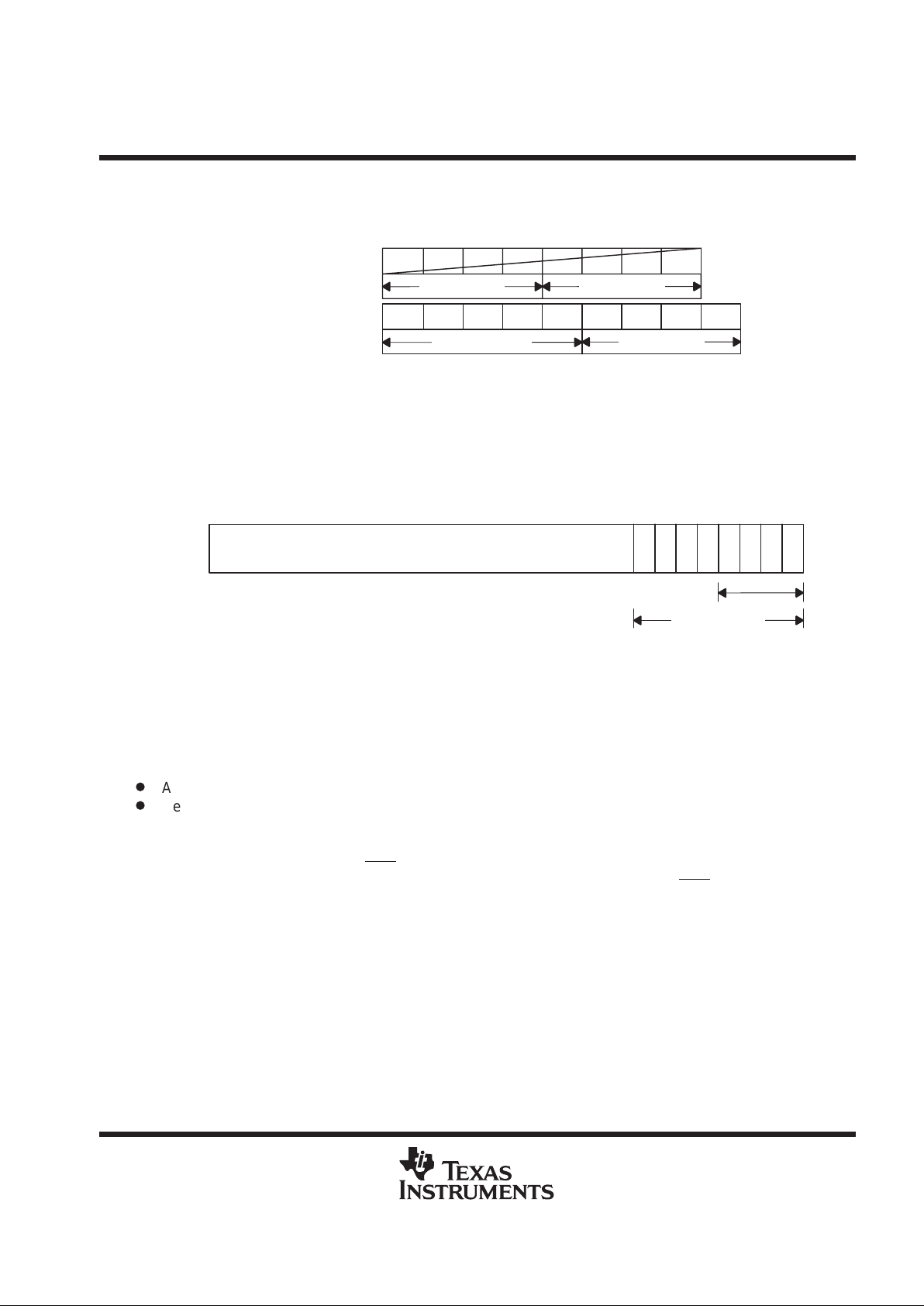
The following are examples of stretch-mode memory operations.
two 32-bit nonpage-mode reads
READADDRREAD
ADDR
4321432143214321
READADDRREADADDR
43214431432443211
2
Stretch Stretch
Stretch Mode Enabled
Stretch Mode Disabled
one 32-bit page-mode read-modify-write
WRITEREADADDR
432143214321
WRITEREADADDR
4324432443211
1
Stretch Stretch
Stretch Mode Enabled
Stretch Mode Disabled
three 32-bit page-mode reads
READREADREADADDR
4321432143214321
READREADREADADDR
4321431432443211
2
Stretch
Stretch Mode Enabled
Stretch Mode Disabled
The stretched cycles are designed to accommodate worst-case 32-bit page-mode accesses, so during some
nonpage-mode memory accesses stretches that are not essential can be generated. For example:
one 32-bit nonpage-mode read-write
WRITEADDRREADADDR
4321432143214321
WRITEADDRREADADDR
43214434432443211
2
Stretch Stretch
Stretch Mode Enabled
Stretch Mode Disabled
1
Stretch
Stretches are inserted in read-modify-write accesses to help ease bus turn-around timings. In the above
example, the second stretch is not needed to help these timings because the read/write turn-around has the
whole of the address cycle to evaluate.
SMJ34020A
GRAPHICS SYSTEM PROCESSOR
SGUS011B – APRIL 1991 – REVISED AUGUST 1995
23
POST OFFICE BOX 1443 • HOUSTON, TEXAS 77251–1443
a clock-stretch timing example, SMJ34020A-32 and 150-ns DRAMs
This example analyzes a memory interface timing parameter. It shows that the clock-stretch mechanism can
be used to allow the SMJ34020A-32 to avoid a timing violation when interfaced to 100-ns VRAMs.
Consider a system with:
D
A SMJ34020A-32, which has a 32-MHz clock input frequency and hence a 125-ns cycle time, so
t
Q
= 31 ns. Timing parameters are taken from this data sheet.
D
A SMJ44C251-10 1 megabit × 1 bit DRAM. Timing parameters are taken from the corresponding
Texas Instruments data sheet.
row address hold data after RAS low, t
h(ADV-REL)
Without clock stretch
SMJ4C1024 t
h(RA)
Hold time, row address valid after RAS low Min = 20 ns
SMJ34020A Parameter 88 Hold time, row address valid after RAS
low Min = tQ – 5 ns = 26 ns
If RAS
is passed through a P AL with a delay of 7 ns, then t
h(RA)
seen by the DRAM is 26 ns – 7 ns = 19 ns.
This violates the 20 ns minimum.
With clock stretch
SMJ34020A
Parameter 88
t
h(ADV-REL)
Hold time, row address valid after RAS low Min = 2tQ – 5 ns = 57 ns
With the same 7-ns PAL delay, the DRAM sees t
h(RA)
as 57 ns – 7ns = 50 ns, which does not violate the
20 ns minimum.
cycle timing examples
The following figures show examples of many of the basic cycles that the SMJ34020A uses for memory access,
VRAM control, multiprocessor bus control, and coprocessor communication. These figures should not be used
to determine specific signal timings, but can be used to see signal relationships for the various cycles. The
Q4 phases that
could
be stretched are marked with an * on the diagrams. The conditions required for the stretch
are:
D
The design uses a SMJ34020A.
D
The CONFIG register’s CSE bit is set to 1.
D
The SMJ34020A is doing either:
a) Any address cycle, or
b) A read data cycle in a read-modify-write sequence
The following remarks apply to memory timing in general. A row address is output on RCA0–RCA12 at the start
of a cycle along with the full address and status on LAD0–LAD31. These remain valid until after the fall of ALTCH
and RAS. The column address is then output on RCA0–RCA12, and LAD0–LAD31 are set to read or write data
for the memory access. During a write, the data and WE
are set valid prior to the falling edge of CAS; the data
remains valid until after WE
and CAS have returned high.
Large memory configurations can require external buffering of the address and data lines. DDIN and DDOUT
coordinate these external buffers with LAD.
During the address output to LAD by the SMJ34020A (Figure 2), the least significant four bits (LAD0–LAD3)
contain a bus-status code. PGMD low at the start of Q2 after RAS low indicates that this memory supports
page-mode operation. LRDY high at the start of Q2 after RAS
low indicates that the cycle can continue without
inserting wait states. DDOUT
returns high after the initial address output on LAD (during Q4), indicating that
a memory read cycle is about to take place.
PAL is a trademark of Advanced Micro Devices, Inc.
SMJ34020A
GRAPHICS SYSTEM PROCESSOR
SGUS011B – APRIL 1991 – REVISED AUGUST 1995
24
POST OFFICE BOX 1443 • HOUSTON, TEXAS 77251–1443
cycle timing examples (continued)
BUSFLT
(see Note B)
LRDY
(see Note B)
DDIN
SF
RCA
CAMD
LCLK2
LCLK1
GI
ALTCH
RAS
CAS
WE
TR/QE
DDOUT
PGMD
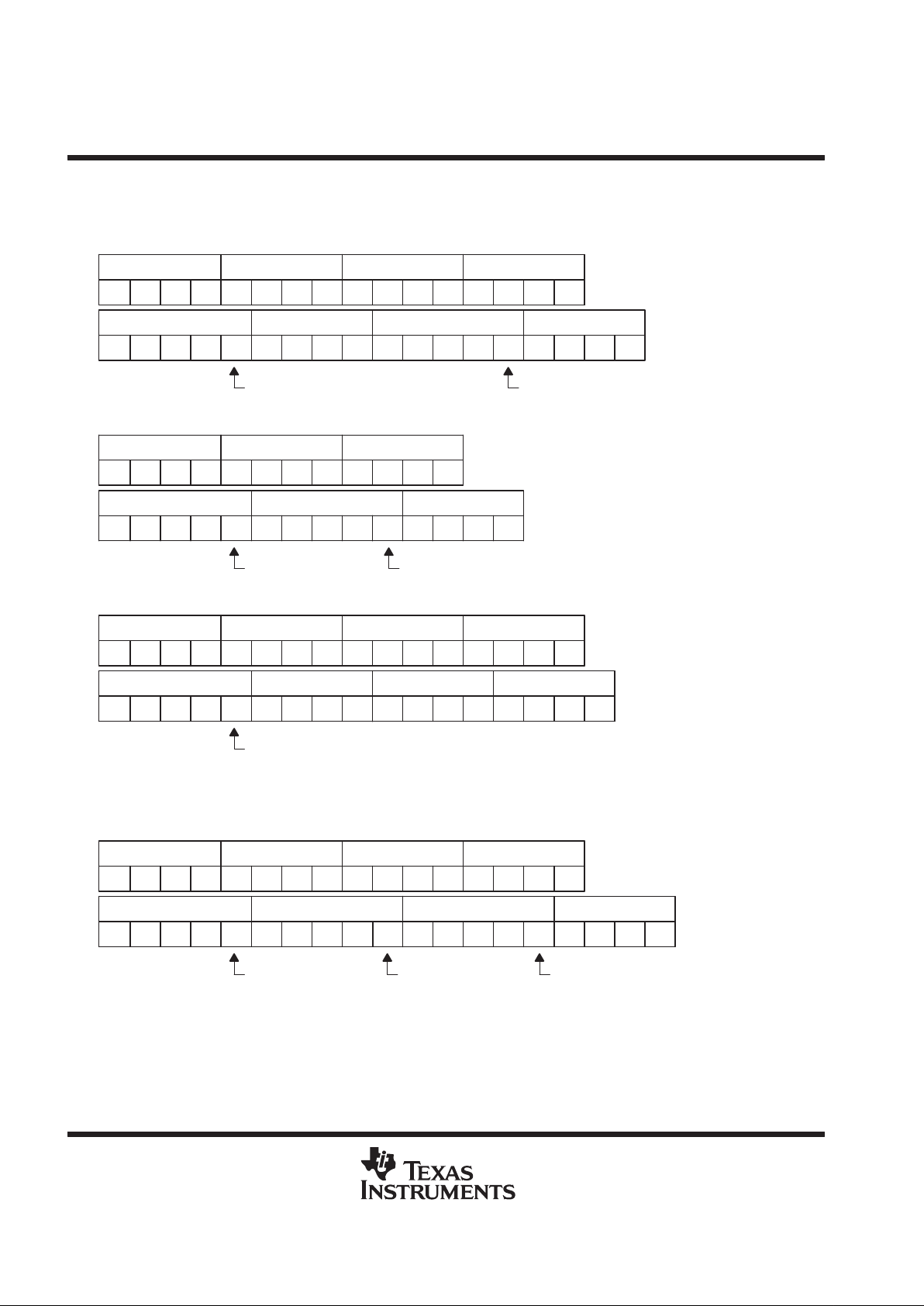
(see Note B)
SIZE16
(see Note B)
Q4 Q1 Q2 Q3 Q1 Q2 Q3 Q4 Q1 Q2 Q3 Q4 Q1
Address
Row 1st Column
2nd Column
Address Subcycle
Data Transfer
Subcycle
Data Transfer
Subcycle
Data Data
R0
R1
Standard Memory Read Cycle
Page-Mode Read
LAD (SMJ34020A)
(see Note A)
LAD (Memory)
(see Note A)
Q4
†
†
See clock stretch, page 20.
NOTES: A. LAD (SMJ34020A): Output to LAD by the SMJ34020A
LAD (memory): Output to LAD by the memory.
B. LRDY, PGMD
, SIZE16, and BUSFLT are not sampled on subsequent page-mode cycle accesses to
32-bit-wide memory space.
Figure 2. Local-Memory Read-Cycle Timing (with page mode)
SMJ34020A
GRAPHICS SYSTEM PROCESSOR
SGUS011B – APRIL 1991 – REVISED AUGUST 1995
25
POST OFFICE BOX 1443 • HOUSTON, TEXAS 77251–1443
cycle timing examples (continued)
LRDY low at the start of the first Q2 after RAS low (Figure 3) indicates that the memory requires the addition
of wait states. LRDY high at the next Q2 indicates the cycle can continue without inserting more wait states.
PGMD
high at the start of Q2 where LRDY is sampled high indicates that this memory does not support
page-mode operation.
LCLCK1
LCLCK2
GI
LAD (SMJ34020A)
LAD (Memory)
CAMD
RCA
ALTCH
RAS
CAS
WE
TR/QE
SF
DDIN
DDOUT
LRDY
PGMD
SIZE16
BUSFLT
R0
R1
Q4 Q1 Q2 Q3 Q1 Q2 Q3 Q4 Q1 Q2 Q3 Q4 Q1
Address
Column
Address Subcycle Wait State Read Transfer
Data
Row
Q4
†
(see Note A)
(see Note A)
(see Note B)
(see Note B)
†
See clock stretch, page 20.
NOTES: A. LAD (SMJ34020A): Output to LAD by the SMJ34020A
LAD (memory): Output to LAD by the memory.
B. Although they are not internally sampled, PGMD
and SIZE16 must be held at a valid level at the
start of each Q2 until LRDY is sampled high.
Figure 3. Local-Memory Read-Cycle Timing (without page mode, with one wait state)

SMJ34020A
GRAPHICS SYSTEM PROCESSOR
SGUS011B – APRIL 1991 – REVISED AUGUST 1995
26
POST OFFICE BOX 1443 • HOUSTON, TEXAS 77251–1443
cycle timing examples (continued)
During the address output to LAD by the SMJ34020A (Figure 4), the least significant four bits (LAD0–LAD3)
contain a bus-status code. PGMD
low at the start of Q2 after RAS low indicates that this memory supports
page-mode operation. LRDY high at the start of Q2 after RAS
low indicates that the cycle can continue without
inserting wait states.
DDOUT
remains low after the initial address output on LAD (during Q4 after RAS goes low), indicating that a
memory write cycle is about to take place.
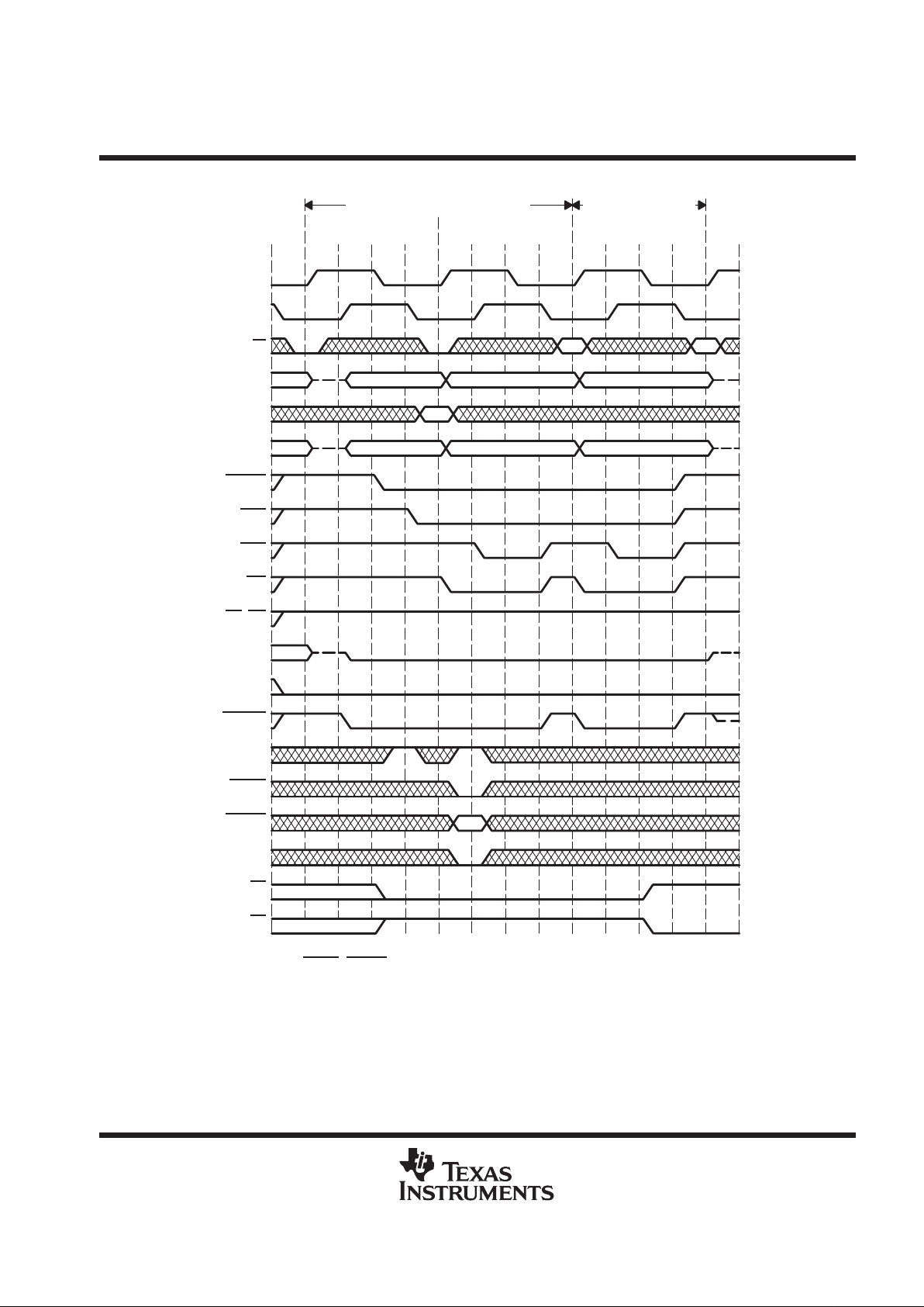
SMJ34020A
GRAPHICS SYSTEM PROCESSOR
SGUS011B – APRIL 1991 – REVISED AUGUST 1995
27
POST OFFICE BOX 1443 • HOUSTON, TEXAS 77251–1443
cycle timing examples (continued)
LCLCK1
LCLCK2
GI
LAD
CAMD
RCA
ALTCH
RAS
CAS
WE
TR/QE
SF
DDIN
DDOUT
LRDY
PGMD
SIZE16
BUSFLT
R0
R1
Q4 Q1 Q2 Q3 Q1 Q2 Q3 Q4 Q1 Q2 Q3 Q4 Q1
Address
Row 1st Column 2nd Column
Address Subcycle
Data Transfer
Subcycle
Data Transfer
Subcycle
Data Out 1 Data Out 2
Standard Memory Write Cycle Page-Mode Write
Q4
†
(see Note A)
(see Note A)
(see Note A)
(see Note A)
†
See clock stretch, page 20.
NOTE A: LRDY, PGMD
, SIZE16, and BUSFLT are not sampled on subsequent page-mode cycle
accesses to 32-bit-wide memory space.
Figure 4. Local-Memory Write-Cycle Timing (With Page Mode)

SMJ34020A
GRAPHICS SYSTEM PROCESSOR
SGUS011B – APRIL 1991 – REVISED AUGUST 1995
28
POST OFFICE BOX 1443 • HOUSTON, TEXAS 77251–1443
cycle timing examples (continued)
The local memory read-modify-write cycle (Figure 5) is used when inserting a field into memory that crosses
byte boundaries. This cycle is actually performed as a read access followed by a page-mode write cycle.
Q4 Q1 Q2 Q3 Q1 Q2 Q3 Q1 Q2 Q3 Q4 Q1
Address
Row Column
Address Subcycle
Data Transfer
Subcycle
Data Transfer
Subcycle
Data
Data Out
Standard Memory Write Cycle Page-Mode Write
LCLCK1
LCLCK2
GI
LAD (SMJ34020A)
LAD (Memory)
CAMD
RCA
ALTCH
RAS
CAS
WE
TR/QE
SF
DDIN
DDOUT
LRDY
PGMD
SIZE16
BUSFLT
R0
R1
Q4 Q4
†
†
See clock stretch, page 20.
Figure 5. Local-Memory Read-Modify-Write-Cycle Timing
 Loading...