


Texas Instruments SN54ABT8996FK, SN54ABT8996JT, SN74ABT8996DWR, SN74ABT8996PWLE, SN74ABT8996PWR Datasheet
...SN54ABT8996, SN74ABT8996 10-BIT ADDRESSABLE SCAN PORTS MULTIDROP-ADDRESSABLE IEEE STD 1149.1 (JTAG) TAP TRANSCEIVERS
SCBS489C ± AUGUST 1994 ± REVISED APRIL 1999
DMembers of Texas Instruments Broad Family of Testability Products Supporting IEEE Std 1149.1-1990 (JTAG) Test Access Port (TAP) and Boundary-Scan Architecture
DExtend Scan Access From Board Level to Higher Levels of System Integration
DPromote Reuse of Lower-Level (Chip/Board) Tests in System Environment
DSwitch-Based Architecture Allows Direct Connect of Primary TAP to Secondary TAP
DPrimary TAP Is Multidrop for Minimal Use of Backplane Wiring Channels
DSimple Addressing (Shadow) Protocol Is Received/Acknowledged on Primary TAP
DShadow Protocols Can Occur in Any of Test-Logic-Reset, Run-Test/Idle, Pause-DR, and Pause-IR TAP States to Provide for Board-to-Board Test and Built-In Self-Test
SN54ABT8996 . . . JT PACKAGE SN74ABT8996 . . . DW OR PW PACKAGE
|
|
|
|
(TOP VIEW) |
|
|
|
|
||
|
A4 |
|
|
|
|
A5 |
||||
|
|
1 |
24 |
|
||||||
|
|
|
||||||||
|
A3 |
|
2 |
23 |
|
A6 |
||||
|
|
|
||||||||
|
A2 |
|
3 |
22 |
|
A7 |
||||
|
|
|
||||||||
|
A1 |
|
4 |
21 |
|
A8 |
||||
|
|
|
||||||||
|
A0 |
|
5 |
20 |
|
A9 |
||||
|
|
|
||||||||
|
|
|
|
|
|
|
|
VCC |
||
|
BYP |
|
|
6 |
19 |
|
||||
GND |
|
7 |
18 |
|
|
CON |
|
|||
PTDO |
|
8 |
17 |
|
STDI |
|||||
|
|
|||||||||
PTCK |
|
9 |
16 |
|
STCK |
|||||
|
|
|||||||||
PTMS |
|
10 |
15 |
|
STMS |
|||||
|
|
|||||||||
PTDI |
|
11 |
14 |
|
STDO |
|||||
|
|
|||||||||
|
|
|
|
|
|
|
|
|
|
|
PTRST |
|
|
|
12 |
13 |
|
|
STRST |
||
|
|
|
|
|
|
|
|
|
|
|
SN54ABT8996 . . . FK PACKAGE
(TOP VIEW)
D 10-Bit Address Space Provides for Up to |
|
A2 |
A3 |
A4 |
NC |
A5 |
A6 |
A7 |
|
|
|
|
|
|
|
|
|
|
|
1021 User-Specified Board Addresses |
|
|
|
|
|
|
|
|
|
D Bypass (BYP) Pin Forces |
A1 |
4 |
3 |
2 |
1 |
28 |
27 26 |
A8 |
|
5 |
|
|
|
|
|
25 |
|||
Primary-to-Secondary Connection Without |
A0 |
6 |
|
|
|
|
|
24 |
A9 |
Use of Shadow Protocols |
BYP |
7 |
|
|
|
|
|
23 |
VCC |
D Connect (CON) Pin Provides Indication of |
|
|
|
|
|
||||
NC |
8 |
|
|
|
|
|
22 |
NC |
|
Primary-to-Secondary Connection |
GND |
9 |
|
|
|
|
|
21 |
CON |
D High-Drive Outputs (±32-mA IOH, 64-mA IOL) |
PTDO |
10 |
|
|
|
|
|
20 |
STDI |
Support Backplane Interface at Primary and |
PTCK |
1112 13 14 15 16 17 1819 |
STCK |
||||||
High Fanout at Secondary |
|
PTMS |
PTDI |
PTRST NC |
STRST |
STDO |
STMS |
|
|
D Package Options Include Plastic Small- |
|
|
|||||||
|
|
|
|
|
|
|
|
|
|
Outline (DW) and Thin Shrink Small- |
|
|
|
|
|
|
|
|
|
Outline (PW) Packages, Ceramic Chip |
NC ± No internal connection |
|
|
|
|||||
Carriers (FK), and Ceramic DIPs (JT) |
|
|
|
||||||
|
|
|
|
|
|
|
|
|
|
description
The 'ABT8996 10-bit addressable scan ports (ASP) are members of the Texas Instruments (TI ) SCOPE testability integrated-circuit family. This family of devices supports IEEE Standard 1149.1-1990 boundary scan to facilitate testing of complex circuit assemblies. Unlike most SCOPE devices, the ASP is not a boundary-scannable device, rather, it applies TI's addressable-shadow-port technology to the IEEE Standard 1149.1-1990 (JTAG) test access port (TAP) to extend scan access beyond the board level.
Conceptually, the ASP is a simple switch that can be used to directly connect a set of multidrop primary TAP signals to a set of secondary TAP signals ± for example, to interface backplane TAP signals to a board-level TAP. The ASP provides all signal buffering that might be required at these two interfaces. When primary and secondary TAPs are connected, only a moderate propagation delay is introduced ± no storage/retiming elements are inserted. This minimizes the need for reformatting board-level test vectors for in-system use.
Please be aware that an important notice concerning availability, standard warranty, and use in critical applications of Texas Instruments semiconductor products and disclaimers thereto appears at the end of this data sheet.
SCOPE is a trademark of Texas Instruments Incorporated.
PRODUCTION DATA information is current as of publication date. Products conform to specifications per the terms of Texas Instruments standard warranty. Production processing does not necessarily include testing of all parameters.
Copyright 1999, Texas Instruments Incorporated
POST OFFICE BOX 655303 •DALLAS, TEXAS 75265 |
1 |

SN54ABT8996, SN74ABT8996
10-BIT ADDRESSABLE SCAN PORTS
MULTIDROP-ADDRESSABLE IEEE STD 1149.1 (JTAG) TAP TRANSCEIVERS
SCBS489C ± AUGUST 1994 ± REVISED APRIL 1999
description (continued)
Most operations of the ASP are synchronous to the primary test clock (PTCK) input. This PTCK signal always is buffered directly onto the secondary test clock (STCK) output.
Upon power up of the device, the ASP assumes a condition in which the primary TAP is disconnected from the secondary TAP (unless the bypass signal is used, as below). This reset condition also can be entered by the assertion of the primary test reset (PTRST) input or by use of shadow protocol. The PTRST signal is always buffered directly onto the secondary test reset (STRST) output, ensuring that the ASP and its associated secondary TAP can be reset simultaneously.
When connected, the primary test data input (PTDI) and primary test mode select (PTMS) input are buffered onto the secondary test data output (STDO) and secondary test mode select (STMS) output, respectively, while the secondary test data input (STDI) is buffered onto the primary test data output (PTDO). When disconnected, STDO is at high impedance, while PTDO is at high impedance, except during acknowledgement of a shadow protocol. Upon disconnect of the secondary TAP, STMS holds its last low or high level, allowing the secondary TAP to be held in its last stable state. Upon reset of the ASP, STMS is high, allowing the secondary TAP to be synchronously reset to the Test-Logic-Reset state.
In system, primary-to-secondary connection is based on shadow protocols that are received and acknowledged on PTDI and PTDO, respectively. These protocols can occur in any of the stable TAP states other than Shift-DR or Shift-IR (i.e., Test-Logic-Reset, Run-Test/Idle, Pause-DR or Pause-IR). The essential nature of the protocols is to receive/transmit an address via a serial bit-pair signaling scheme. When an address is received serially at PTDI that matches that at the parallel address inputs (A9±A0), the ASP serially retransmits its address at PTDO as an acknowledgement and then assumes the connected (ON) status, as above. If the received address does not match that at the address inputs, the ASP immediately assumes the disconnected (OFF) status without acknowledgement.
The ASP also supports three dedicated addresses that can be received globally (that is, to which all ASPs respond) during shadow protocols. Receipt of the dedicated disconnect address (DSA) causes the ASP to disconnect in the same fashion as a non-matching address. Reservation of this address for global use ensures that at least one address is available to disconnect all receiving ASPs. The DSA is especially useful when the secondary TAPs of multiple ASPs are to be left in different stable states. Receipt of the reset address (RSA) causes the ASP to assume the reset condition, as above. Receipt of the test-synchronization address (TSA) causes the ASP to assume a connect status (MULTICAST) in which PTDO is at high impedance but the connections from PTMS to STMS and PTDI to STDO are maintained to allow simultaneous operation of the secondary TAPs of multiple ASPs. This is useful for multicast TAP-state movement, simultaneous test operation (such as in Run-Test/Idle state), and scanning of common test data into multiple like scan chains. The TSA is valid only when received in the Pause-DR or Pause-IR TAP states.
Alternatively, primary-to-secondary connection can be selected by assertion of a low level at the bypass (BYP) input. This operation is asynchronous to PTCK and is independent of PTRST and/or power-up reset. This bypassing feature is especially useful in the board-test environment, since it allows the board-level automated test equipment (ATE) to treat the ASP as a simple transceiver. When the BYP input is high, the ASP is free to respond to shadow protocols. Otherwise, when BYP is low, shadow protocols are ignored.
Whether the connected status is achieved by use of shadow protocol or by use of BYP, this status is indicated by a low level at the connect (CON) output. Likewise, when the secondary TAP is disconnected from the primary TAP, the CON output is high.
The SN54ABT8996 is characterized for operation over the full military temperature range of ±55°C to 125°C. The SN74ABT8996 is characterized for operation from ±40°C to 85°C.
2 |
POST OFFICE BOX 655303 •DALLAS, TEXAS 75265 |

SN54ABT8996, SN74ABT8996 10-BIT ADDRESSABLE SCAN PORTS MULTIDROP-ADDRESSABLE IEEE STD 1149.1 (JTAG) TAP TRANSCEIVERS
SCBS489C ± AUGUST 1994 ± REVISED APRIL 1999
FUNCTION TABLE
|
INPUTS |
SHADOW-PROTOCOL |
|
|
|
|
OUTPUTS |
|
|
|
PRIMARY-TO-SECONDARY |
|||||
|
|
|
|
|
RESULT² |
|
|
|
STCK |
STMS |
STDO |
PTDO |
|
|
CONNECT STATUS |
|
|
BYP |
|
PTRST |
|
|
STRST |
|
CON |
|
|||||||
|
L |
|
L |
Ð |
|
L |
PTCK |
H³ |
|
PTDI |
STDI |
L |
BYP/TRST³ |
|||
|
L |
|
H |
Ð |
|
H |
PTCK |
PTMS |
PTDI |
STDI |
L |
BYP |
||||
|
H |
|
L |
Ð |
|
L |
PTCK |
H |
|
Z |
Z |
H |
TRST |
|||
|
H |
|
H |
RESET |
|
H |
PTCK |
H |
|
Z |
Z |
H |
RESET |
|||
|
H |
|
H |
MATCH |
|
H |
PTCK |
PTMS |
PTDI |
STDI |
L |
ON |
||||
|
H |
|
H |
NO MATCH |
|
H |
PTCK |
STMS |
§ |
Z |
Z |
H |
OFF |
|||
|
|
|
|
|
|
|
|
|
|
|
0 |
|
|
|
|
|
|
H |
|
H |
HARD ERROR¶ |
|
H |
PTCK |
STMS |
§ |
Z |
Z |
H |
OFF |
|||
|
|
|
|
|
|
|
|
|
|
|
0 |
|
|
|
|
|
|
H |
|
H |
DISCONNECT |
|
H |
PTCK |
STMS |
§ |
Z |
Z |
H |
OFF |
|||
|
|
|
|
|
|
|
|
|
|
|
0 |
|
|
|
|
|
|
H |
|
H |
TEST SYNCHRONIZATION |
|
H |
PTCK |
PTMS |
PTDI |
Z |
L |
MULTICAST |
||||
²Shadow protocols are received serially via PTCK and PTDI and acknowledged serially via PTCK and PTDO under certain conditions in which PTMS is static low or static high (see shadow protocol). The result shown here follows any required acknowledgement.
³In normal operation of IEEE Std 1149.1-compliant architectures, it is recommended that TMS be high prior to release of TRST. The BYP/TRST connect status ensures that this condition is met at STMS regardless of the applied PTMS. Also, it is recommended that STMS be kept high for a minimum duration of 5 PTCK cycles following assertion of PTRST, either by maintaining PTRST low or by setting PTMS high. This ensures that ICs both with and without TRST inputs are moved to their Test-Logic-Reset TAP states. It is expected that in normal application, this condition
will only occur when BYP is fixed at the low state. In such case, upon release of PTRST, the ASP immediately resumes the BYP connect status. § STMS level before indicated steady-state conditions were established
¶The shadow protocol is well defined. Some variations in the protocol are tolerated (see protocol errors). Those that are not tolerated are considered hard errors and cause disconnect as indicated.
functional block diagram
PTCK |
9 |
|
16 |
STCK |
|
VCC |
|
|
|
PTRST |
12 |
|
13 |
STRST |
|
VCC |
|
S |
|
|
|
|
|
|
PTMS |
10 |
|
15 |
STMS |
VCC |
|
1D |
||
|
|
C1 |
|
|
|
|
|
|
|
PTDI |
11 |
|
14 |
STDO |
|
VCC |
|
|
|
STDI |
17 |
|
|
|
|
VCC |
|
8 |
PTDO |
|
|
|
|
|
BYP |
6 |
|
|
|
|
|
|
|
|
|
|
Shadow-Protocol |
|
|
|
|
Receive |
|
|
|
VCC |
Connect Control |
18 |
CON |
|
20±24, |
|
||
|
|
|
||
|
|
|
|
|
A9±A0 |
1±5 |
|
|
|
|
|
Shadow-Protocol |
|
|
|
|
Transmit |
|
|
Pin numbers shown are for the DW, JT, and PW packages.
POST OFFICE BOX 655303 •DALLAS, TEXAS 75265 |
3 |

SN54ABT8996, SN74ABT8996
10-BIT ADDRESSABLE SCAN PORTS
MULTIDROP-ADDRESSABLE IEEE STD 1149.1 (JTAG) TAP TRANSCEIVERS
SCBS489C ± AUGUST 1994 ± REVISED APRIL 1999
|
|
|
|
|
|
|
|
|
|
|
|
|
|
Terminal Functions |
|||||||
|
|
|
|
|
|
|
|
|
|
|
|
|
|
|
|
|
|
|
|
|
|
TERMINAL |
|
|
|
|
|
|
|
|
|
|
|
DESCRIPTION |
|||||||||
|
NAME |
|
|
|
|
|
|
|
|
|
|
|
|||||||||
|
|
|
|
|
|
|
|
|
|
|
|
|
|
|
|
||||||
|
|
|
|
|
|
|
|
|
|
|
|
|
|
|
|
|
|
|
|
|
|
|
|
|
|
|
|
|
Address inputs. The ASP compares addresses received via shadow protocol against the value at A9±A0 to determine |
||||||||||||||
|
A9±A0 |
address match. The bit order is from most significant to least significant. An internal pullup at each A9±A0 terminal forces |
|||||||||||||||||||
|
|
|
|
|
|
|
the terminal to a high level if it has no external connection. |
||||||||||||||
|
|
|
|
|
|
|
|
|
|
|
|
|
|
|
|
|
|
|
|
||
|
|
|
|
|
|
|
Bypass input. A low input at |
|
|
forces the ASP into BYP or BYP/TRST status, depending on |
|
being high or |
|||||||||
|
|
|
|
|
|
|
BYP |
PTRST |
|||||||||||||
|
|
|
BYP |
|
|
|
low, respectively. While BYP is low, shadow protocols are ignored. Otherwise, while BYP is high, the ASP is free to |
||||||||||||||
|
|
|
|
|
|
|
respond to shadow protocols. An internal pullup forces BYP to a high level if it has no external connection. |
||||||||||||||
|
|
|
|
|
|
|
|
|
|
|
|
|
|
|
|
|
|
||||
|
|
|
|
|
|
|
Connect indicator (output). The ASP indicates secondary-scan-port activity (resulting from BYP, BYP/TRST, |
||||||||||||||
|
|
CON |
|
|
MULTICAST, or ON status) by forcing CON to be low. Inactivity (resulting from OFF, RESET, or TRST status) is indicated |
||||||||||||||||
|
|
|
|
|
|
|
when CON is high. |
||||||||||||||
|
|
|
|
|
|
|
|
|
|
|
|
|
|
|
|||||||
|
|
GND |
Ground |
||||||||||||||||||
|
|
|
|
|
|
|
|
|
|
|
|
|
|
|
|
|
|
||||
|
|
|
|
|
|
|
Primary test clock. PTCK receives the TCK signal required by IEEE Standard 1149.1-1990. The ASP always buffers |
||||||||||||||
|
PTCK |
PTCK to STCK. Shadow protocols are received/acknowledged synchronously to PTCK and connect-status changes |
|||||||||||||||||||
|
|
|
|
|
|
|
invoked by shadow protocol are made synchronously to PTCK. |
||||||||||||||
|
|
|
|
|
|
|
|
|
|
|
|
|
|
|
|
|
|
||||
|
|
|
|
|
|
|
Primary test data input. PTDI receives the TDI signal required by IEEE Standard 1149.1-1990. During appropriate TAP |
||||||||||||||
|
|
|
|
|
|
|
states, the ASP monitors PTDI for shadow protocols. During shadow protocols, data at PTDI is captured on the rising |
||||||||||||||
|
PTDI |
edge of PTCK. When a valid shadow protocol is received in this fashion, the ASP compares the received address against |
|||||||||||||||||||
|
the A9±A0 inputs. If the ASP detects a match, it outputs an acknowledgement and then connects its primary TAP |
||||||||||||||||||||
|
|
|
|
|
|
|
|||||||||||||||
|
|
|
|
|
|
|
terminals to its secondary TAP terminals. Under BYP, BYP/TRST, MULTICAST or ON status, the ASP buffers the PTDI |
||||||||||||||
|
|
|
|
|
|
|
signal to STDO. An internal pullup forces PTDI to a high level if it has no external connection. |
||||||||||||||
|
|
|
|
|
|
|
|
|
|
|
|
|
|
|
|
|
|
||||
|
|
|
|
|
|
|
Primary test data output. PTDO transmits the TDO signal required by IEEE Standard 1149.1-1990. During shadow |
||||||||||||||
|
PTDO |
protocols, the ASP transmits any required acknowledgement via the PTDO. The acknowledgement data output at PTDO |
|||||||||||||||||||
|
changes on the falling edge of PTCK. Under BYP, BYP/TRST, or ON status, the ASP buffers the PTDO signal from STDI. |
||||||||||||||||||||
|
|
|
|
|
|
|
|||||||||||||||
|
|
|
|
|
|
|
Under OFF, MULTICAST, RESET, or TRST status, PTDO is at high impedance. |
||||||||||||||
|
|
|
|
|
|
|
|
|
|
|
|
|
|
|
|
|
|
||||
|
|
|
|
|
|
|
Primary test mode select. PTMS receives the TMS signal required by IEEE Standard 1149.1-1990. The ASP monitors |
||||||||||||||
|
|
|
|
|
|
|
the PTMS to determine the TAP-controller state. During stable TAP states other than Shift-DR or Shift-IR (i.e., |
||||||||||||||
|
PTMS |
Test-Logic-Reset, Run-Test-Idle, Pause-DR, Pause-IR) the ASP can respond to shadow protocols. Under BYP, |
|||||||||||||||||||
|
|
|
|
|
|
|
MULTICAST, or ON status, the ASP buffers the PTMS signal to STMS. An internal pullup forces PTMS to a high level |
||||||||||||||
|
|
|
|
|
|
|
if it has no external connection. |
||||||||||||||
|
|
|
|
|
|
|
|
|
|
|
|
|
|
|
|
||||||
|
|
|
|
|
|
|
Primary test reset. |
|
|
|
receives the |
|
|
signal allowed by IEEE Standard 1149.1-1990. The ASP always buffers |
|||||||
|
|
|
|
|
|
|
PTRST |
TRST |
|
||||||||||||
|
|
|
|
|
|
|
PTRST to STRST. A low input at PTRST forces the ASP to assume TRST or BYP/TRST status, depending on BYP being |
||||||||||||||
|
PTRST |
|
high or low, respectively. Such operation also asynchronously resets the internal ASP state to its power-up condition. |
||||||||||||||||||
|
|
|
|
|
|
|
Otherwise, while PTRST is high, the ASP is free to respond to shadow protocols. An internal pullup forces PTRST to |
||||||||||||||
|
|
|
|
|
|
|
a high level if it has no external connection. |
||||||||||||||
|
|
|
|
|
|
|
|
|
|
|
|
|
|
||||||||
|
STCK |
Secondary test clock. STCK retransmits the TCK signal required by IEEE Standard 1149.1-1990. The ASP always |
|||||||||||||||||||
|
buffers STCK from PTCK. |
||||||||||||||||||||
|
|
|
|
|
|
|
|||||||||||||||
|
|
|
|
|
|
|
|
|
|
|
|
|
|
||||||||
|
|
|
|
|
|
|
Secondary test data input. STDI receives the TDI signal required by IEEE Standard 1149.1-1990. Under BYP, |
||||||||||||||
|
STDI |
BYP/TRST, or ON status, the ASP buffers STDI to PTDO. An internal pullup forces STDI to a high level if it has no external |
|||||||||||||||||||
|
|
|
|
|
|
|
connection. |
||||||||||||||
|
|
|
|
|
|
|
|
|
|
|
|
|
|
||||||||
|
|
|
|
|
|
|
Secondary test data output. STDO transmits the TDO signal required by IEEE Standard 1149.1-1990. Under BYP, |
||||||||||||||
|
STDO |
BYP/TRST, MULTICAST, or ON status, the ASP buffers STDO from PTDI. Under OFF, RESET, or TRST status, STDO |
|||||||||||||||||||
|
|
|
|
|
|
|
is at high impedance. |
||||||||||||||
|
|
|
|
|
|
|
|
|
|
|
|
|
|
||||||||
|
|
|
|
|
|
|
Secondary test mode select. STMS retransmits the TMS signal required by IEEE Standard 1149.1-1990. Under BYP, |
||||||||||||||
|
STMS |
MULTICAST, or ON status, the ASP buffers STMS from PTMS. When disconnected (as a result of OFF status), STMS |
|||||||||||||||||||
|
maintains its last valid state until the ASP assumes BYP/TRST, RESET, or TRST status (upon which it is forced high) |
||||||||||||||||||||
|
|
|
|
|
|
|
|||||||||||||||
|
|
|
|
|
|
|
or the ASP again assumes BYP, MULTICAST, or ON status. |
||||||||||||||
|
|
|
|
|
|
|
|
|
|
|
|
|
|
||||||||
|
|
|
|
|
|
|
|
|
|
|
|
||||||||||
|
|
|
|
|
|
|
Secondary test reset. |
STRST |
retransmits the |
TRST |
signal allowed by IEEE Standard 1149.1-1990. The ASP always |
||||||||||
|
STRST |
||||||||||||||||||||
|
|
|
|
|
|
|
|
|
|
|
|
|
|
|
|
||||||
|
buffers STRST from PTRST. |
||||||||||||||||||||
|
|
|
|
|
|
|
|||||||||||||||
|
|
|
|
||||||||||||||||||
|
|
VCC |
Supply voltage |
||||||||||||||||||
4 |
POST OFFICE BOX 655303 •DALLAS, TEXAS 75265 |

SN54ABT8996, SN74ABT8996 10-BIT ADDRESSABLE SCAN PORTS MULTIDROP-ADDRESSABLE IEEE STD 1149.1 (JTAG) TAP TRANSCEIVERS
SCBS489C ± AUGUST 1994 ± REVISED APRIL 1999
application information
In application, the ASP is used at each of several (serially-chained) groups of IEEE Std 1149.1-compliant devices. The ASP for each such group is assigned an address (via inputs A9±A0) that is unique from that assigned to ASPs for the remaining groups. Each ASP is wired at its primary TAP to common (multidrop) TAP signals (sourced from a central IEEE Std 1149.1 bus master) and fans out its secondary TAP signals to the specific group of IEEE Std 1149.1-compliant devices with which it is associated. An example is shown in Figure 1.
|
|
IEEE Std 1149.1- |
|
|
IEEE Std 1149.1- |
|
|
IEEE Std 1149.1- |
|||||||||
|
|
|
Compliant |
|
|
|
Compliant |
|
|
|
Compliant |
||||||
|
|
|
Device Chain |
|
|
|
Device Chain |
|
|
|
Device Chain |
||||||
|
|
STDI |
STCK |
STMS STDO |
STRST |
|
|
STDI |
STCK |
STMS STDO |
STRST |
|
|
STDI |
STCK |
STMS STDO |
STRST |
ADDR1 |
A9±A0 |
|
|
|
|
ADDR2 |
A9±A0 |
|
|
|
|
ADDR3 |
A9±A0 |
|
|
|
|
|
|
|
ASP |
|
|
|
|
ASP |
|
|
|
|
ASP |
|
|||
|
|
|
|
|
|
|
|
|
|
|
|
|
|
|
|||
|
BYP |
PTDO |
PTCK |
PTMS PTDI |
PTRST |
|
BYP |
PTDO |
PTCK |
PTMS PTDI |
PTRST |
|
BYP |
PTDO |
PTCK |
PTMS PTDI |
PTRST |
|
|
TDI |
|
|
|
|
|
|
|
|
|
|
|
|
|
|
|
IEEE |
TCK |
|
|
Std |
To |
||
TMS |
|||
1149.1 |
Other |
||
TDO |
|||
Bus |
Modules |
||
Master |
TRST |
|
Figure 1. ASP Application
This application allows the ASP to be wired to a 4- or 5-wire multidrop test access bus, such as might be found on a backplane. Each ASP would then be located on a module, for example a printed-circuit board (PCB), which contains a serial chain of IEEE Std 1149.1-compliant devices and which would plug into the module-to-module bus (e.g., backplane). In the complete system, the ASP shadow protocols would allow the selection of the scan chain on a single module. The selected scan chain could then be controlled, via the multidrop TAP, as if it were the only scan chain in the system. Normal IR and DR scans can then be performed to accomplish the module test objectives.
Once scan operations to a given module are complete, another module can be selected in the same fashion, at which time the ASP-based connection to the first module is dissolved. This procedure can be continued progressively for each module to be tested. Finally, one of two global addresses can be issued to either leave all modules unselected (disconnect address, DSA) or to deselect and reset scan chains for all modules (reset address, RSA).
Additionally, in Pause-DR and Pause-IR TAP states, a third global address (test-synchronization address, TSA) can be invoked to allow simultaneous TAP-state changes and multicast scan-in operations to selected modules. This is especially useful in the former case, for allowing selected modules to be moved simultaneously to the Run-Test-Idle TAP state for module-level or module-to-module built-in self-test (BIST) functions, which operate synchronously to TCK in that TAP state, and in the latter case, for scanning common test setup/data into multiple like modules.
POST OFFICE BOX 655303 •DALLAS, TEXAS 75265 |
5 |
SN54ABT8996, SN74ABT8996
10-BIT ADDRESSABLE SCAN PORTS
MULTIDROP-ADDRESSABLE IEEE STD 1149.1 (JTAG) TAP TRANSCEIVERS
SCBS489C ± AUGUST 1994 ± REVISED APRIL 1999
architecture
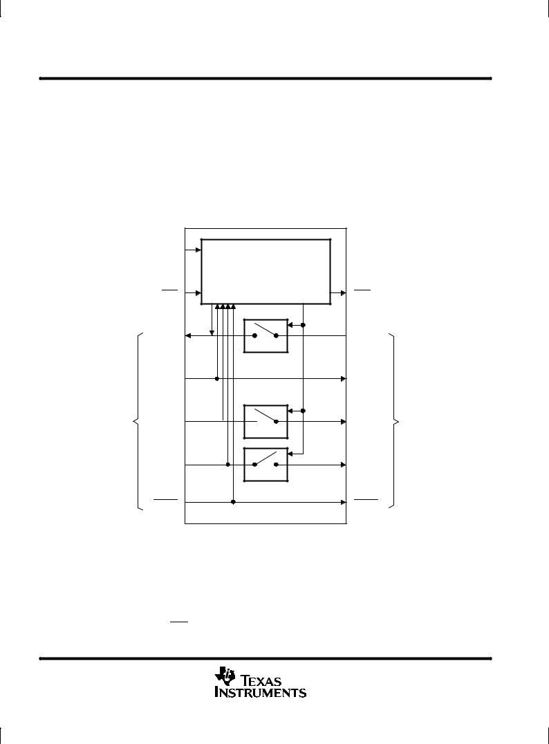
Conceptually, the ASP can be viewed as a bank of switches that can connect or isolate a module-level TAP to/from a higher-level (e.g., module-to-module) TAP. This is shown in Figure 2. The state of the switches (open versus closed) is based on shadow protocols, which are received on PTDI and are synchronous to PTCK.
The simple architecture of the ASP allows the system designer to overcome the limitations of IEEE Std 1149.1 ring and star configurations. Ring configurations (in which each module's TDO is chained to the next module's TDI) are of limited use in backplane environments, since removal of a module breaks the scan chain and prevents test of the remainder of the system. Star configurations (in which all module TDOs and TDIs are connected in parallel) are suited to the backplane environment, but, since each module must receive its own TMS, are costly in terms of backplane routing channels. By comparison, use of the ASP allows all five IEEE Std 1149.1 signals to be routed in multidrop fashion.
From Multidrop,
Module-to-Module
Test Access Port
A9±A0
Control
BYP
PTDO
PTCK
1 PTMS
PTMS 

0
PTDI
PTRST
Figure 2. ASP Conceptual Model
CON
STDI
STCK |
|
|
STMS |
To Module-Level |
|
Test Access Port |
||
|
STDO
STRST
As shown in the functional block diagram, the ASP comprises three major logic blocks. Blocks for shadow-protocol receive and shadow-protocol transmit are responsible for receipt of select protocol and transmission of acknowledge protocol, respectively. The connect-control block is responsible for TAP-state monitor and address matching.
Some additional logic is illustrated outside of these major blocks. This additional logic is responsible for controlling the activity of the ASP outputs based on the shadow-protocol result and/or protocol bypass [as selected by an active (low) BYP input].
6 |
POST OFFICE BOX 655303 •DALLAS, TEXAS 75265 |

SN54ABT8996, SN74ABT8996 10-BIT ADDRESSABLE SCAN PORTS MULTIDROP-ADDRESSABLE IEEE STD 1149.1 (JTAG) TAP TRANSCEIVERS
SCBS489C ± AUGUST 1994 ± REVISED APRIL 1999
shadow protocol
Addressing of an ASP in system is accomplished by shadow protocols, which are received at PTDI synchronously to PTCK. Shadow protocols can occur only in the following stable TAP states: Test-Logic-Reset, Run-Test/Idle, Pause-DR, and Pause-IR. Shadow protocols never occur in Shift-DR or Shift-IR states in order to prevent contention on the signal bus to which PTDO is wired. Additionally, the ASP PTMS must be held at a constant low or high level throughout a shadow protocol. If TAP-state changes occur in the midst of a shadow protocol, the shadow protocol is aborted and the select-protocol state machine returns to its initial state.
The shadow protocol is based on a serial bit-pair signaling scheme in which two bit-pair combinations (data one, data zero) are used to represent address data and the other two bit-pair combinations (select, idle) are used for framing ± that is, to indicate where address data begins and ends.
These bit pairs are received serially at PTDI (or transmitted serially at PTDO) synchronously to PTCK as follows:
±The idle bit pair (I) is represented as two consecutive high signals.
±The select bit pair (S) is represented as two consecutive low signals.
±The data-one bit pair (D) is represented as a low signal followed by a high signal.
±The data-zero bit pair (D) is represented as a high signal followed by a low signal.
PTDI or PTDO
PTCK
First Bit of Pair Is Transmitted
First Bit of Pair Is Received
Second Bit of Pair Is Transmitted
Second Bit of Pair Is Received
Figure 3. Bit-Pair Timing (Data Zero Shown)
A complete shadow protocol is composed of the receipt of a select protocol followed, if applicable, by the transmission of an acknowledge protocol (which is issued from PTDO only if the received address matches that at the A9±A0 inputs). Both of these subprotocols are composed of ten data bit pairs framed at the beginning by idle and select bit pairs and at the end by select and idle bit pairs. This is represented in an abbreviated fashion as follows: ISDDDDDDDDDDSI. Figure 4 shows a complete shadow protocol (the symbol T is used to represent a high-impedance condition on the associated signal line ± since the high-impedance state at PTDI is logically high due to pullup, it maps onto the idle bit pair).
Received at PTDI
Transmitted at PTDO
Primary Tap Is Inactive
Select Protocol Begins
Select Protocol Ends
Acknowledge Protocol Begins
Acknowledge Protocol Ends
Primary-to-Secondary Connect,
Scan Operations Can Be Initiated
T I S D D D D D D D D D D S I T T T T T T T T T T T T T T T T T T T T T T T T T T T T T T I S D D D D D D D D D D S I T
|
|
|
|
|
|
|
|
|
|
|
|
|
|
LSB |
MSB |
|
LSB |
MSB |
|
||||
|
|
|
|
|
|
|
|
|
|
|
|
|
|
|
|
|
|
|
|
|
|
|
|
|
|
|
|
|
|
|
|
|
|
|
|
|
|
|
|
|
|
|
|
|
|
|
|
Figure 4. Complete Shadow Protocol
POST OFFICE BOX 655303 •DALLAS, TEXAS 75265 |
7 |

SN54ABT8996, SN74ABT8996
10-BIT ADDRESSABLE SCAN PORTS
MULTIDROP-ADDRESSABLE IEEE STD 1149.1 (JTAG) TAP TRANSCEIVERS
SCBS489C ± AUGUST 1994 ± REVISED APRIL 1999
select protocol
The select protocol is the ASP's means of receiving (at PTDI) address information from an IEEE Std 1149.1 bus master. It follows the ISDDDDDDDDDDSI sequence described previously. A 10-bit address value is decoded from the received data-one and/or data-zero bit pairs. These bit pairs are interpreted in least-significant-bit-first order (that is, the first data bit pair received is considered to correspond to A0).
acknowledge protocol
Following the receipt of a complete select-protocol sequence, the protocol result provisionally is set to NO MATCH and the connect status set to OFF. The received address is then compared to that at the ASP address inputs (A9±A0). If these address values match, the ASP immediately (with no delay) responds with an acknowledge protocol transmitted from PTDO. This protocol follows the ISDDDDDDDDDDSI sequence described previously. The transmitted address represents the address of the selected ASP which, by definition, is the same address the ASP received in the select protocol. The 10-bit address value is encoded into data-one and/or data-zero bit pairs. The bit pairs are to be interpreted in least-significant-bit-first order (that is, the first data bit pair transmitted is to be considered to correspond to A0). If the received address does not match that at the A9±A0 inputs, no acknowledge protocol is transmitted and the shadow protocol is considered complete.
protocol errors
Protocol errors occur when bit pairs are received out of sequence. Some of these sequencing errors can be tolerated and are termed soft errors. No specific action occurs as the result of a soft error. Other errors represent cases where the addressing information could be incorrectly received and are termed hard errors. Hard errors are characterized by sequences in which at least one bit of address data has been properly transmitted followed by a sequencing error. When a hard error occurs, any connection to an ASP is dissolved.
Table 1 lists the bit-pair sequences that result in soft errors and hard errors. A hard error also results when the primary TAP state changes during select protocol following the proper transmission of at least one bit of address data. Figures 16 and 17 show shadow-protocol timing in case of protocol hard error while Figure 18 shows shadow-protocol timing in case of protocol soft error.
Table 1. Shadow-Protocol Errors²
SOFT ERRORS HARD ERRORS |
||
I(D)I |
|
|
I(D)(S)I |
|
|
I(D)(S)(D)I |
IS(D)I |
|
IS(D)S(D)I |
||
I(S)I |
||
IS(D)S(S)I |
||
|
||
IS(S)(D)I |
|
|
IS(S)(D)(S)I
²A bit-pair token in parentheses represents one or more instances.
long address
Receipt of an address longer than ten bits is considered a hard error and the ASP assumes OFF status. The sole exceptions are when all data ones are received or all data zeros are received. In these special cases, the global addresses represented by these bit sequences are observed and appropriate action taken. That is, in the case that only data ones (ten or more) are received, the shadow-protocol result is TEST SYNCHRONIZATION (if the primary TAP state is Pause-DR or Pause-IR), and in the case that only data zeros (ten or more) are received, the shadow-protocol result is RESET (see test-synchronization address and reset address).
short address
In all cases, receipt of an address shorter than ten bits is considered a hard error and the ASP assumes OFF status.
8 |
POST OFFICE BOX 655303 •DALLAS, TEXAS 75265 |

SN54ABT8996, SN74ABT8996 10-BIT ADDRESSABLE SCAN PORTS MULTIDROP-ADDRESSABLE IEEE STD 1149.1 (JTAG) TAP TRANSCEIVERS
SCBS489C ± AUGUST 1994 ± REVISED APRIL 1999
connect control
The connect-control block monitors the primary TAP state to enable receipt/acknowledge of shadow protocols in appropriate states (namely, the stable, non-Shift TAP states: Test-Logic-Reset, Run-Test/Idle, Pause-DR, and Pause-IR). Upon receipt of a valid shadow protocol, this block performs the address matching required to compute the shadow-protocol result.
TAP-state monitor
The TAP-state monitor is a synchronous finite-state machine that monitors the primary TAP state. The state diagram is shown in Figure 5 and mirrors that specified by IEEE Standard 1149.1-1990. The TAP-state monitor proceeds through its states based on the level of PTMS at the rising edge of PTCK. Each state is described both in terms of its significance for ASP devices and for connected IEEE Std 1149.1-compliant devices (called targets). However, the monitor state (primary TAP) can be different from that of disconnected scan chains (secondary TAP).
Test-Logic-Reset |
|
|
|
|
PTMS = H |
|
|
|
|
PTMS = L |
|
|
|
|
PTMS = H |
|
PTMS =H |
PTMS = H |
|
Run-Test /Idle |
Select-DR-Scan |
Select-IR-Scan |
||
PTMS = L |
|
PTMS = L |
|
PTMS = L |
|
|
|
||
|
|
PTMS = H |
PTMS = H |
|
|
Capture-DR |
Capture-IR |
||
|
|
PTMS = L |
|
PTMS = L |
PTMS = L |
Shift-DR |
|
Shift-IR |
|
|
|
|
PTMS = L |
|
|
|
PTMS = H |
|
PTMS = H |
PTMS = H |
|
|
|
PTMS = H |
|
Exit1-DR |
Exit1-IR |
||
|
|
PTMS = L |
|
PTMS = L |
|
Pause-DR |
Pause-IR |
||
PTMS = L |
|
|
|
PTMS = L |
|
|
PTMS = H |
PTMS = L |
PTMS = H |
|
|
PTMS = L |
|
|
|
Exit2-DR |
Exit2-IR |
||
|
|
PTMS = H |
|
PTMS = H |
|
Update-DR |
Update-IR |
||
PTMS = H |
PTMS = L |
PTMS = H |
PTMS = L |
|
Figure 5. TAP-Monitor State Diagram
POST OFFICE BOX 655303 •DALLAS, TEXAS 75265 |
9 |

SN54ABT8996, SN74ABT8996
10-BIT ADDRESSABLE SCAN PORTS
MULTIDROP-ADDRESSABLE IEEE STD 1149.1 (JTAG) TAP TRANSCEIVERS
SCBS489C ± AUGUST 1994 ± REVISED APRIL 1999
Test-Logic-Reset
The ASP TAP-state monitor powers up in the Test-Logic-Reset state. Alternatively, the ASP can be forced asynchronously to this state by assertion of its PTRST input. In the stable Test-Logic-Reset state, the ASP is enabled to receive and respond to shadow protocols. The ASP does not recognize the TSA in this state.
For a target device in the stable Test-Logic-Reset state, the test logic is reset and is disabled so that the normal logic function of the device is performed. The instruction register is reset to an opcode that selects the optional IDCODE instruction, if supported, or the BYPASS instruction. Certain data registers also can be reset to their power-up values.
Run-Test/Idle
In the stable Run-Test/Idle state, the ASP is enabled to receive and respond to shadow protocols. The ASP does not recognize the TSA in this state.
For a target device, Run-Test/Idle is a stable state in which the test logic can be actively running a test or can be idle.
Select-DR-Scan, Select-lR-Scan
The ASP is not enabled to receive and respond to shadow protocols in the Select-DR-Scan and Select-lR-Scan states.
For a target device, no specific function is performed in the Select-DR-Scan and Select-lR-Scan states, and the TAP controller exits either of these states on the next TCK cycle. These states allow the selection of either data-register scan or instruction-register scan.
Capture-DR
The ASP is not enabled to receive and respond to shadow protocols in the Capture-DR state.
For a target device in the Capture-DR state, the selected data register can capture a data value as specified by the current instruction. Such capture operations occur on the rising edge of TCK, upon which the Capture-DR state is exited.
Shift-DR
The ASP is not enabled to receive and respond to shadow protocols in the Shift-DR state.
For a target device, upon entry to the Shift-DR state, the selected data register is placed in the scan path between TDI and TDO, and on the first falling edge of TCK, TDO goes from the high-impedance state to an active state. TDO outputs the logic level present in the least-significant bit of the selected data register. While in the stable Shift-DR state, data is serially shifted through the selected data register on each TCK cycle.
Exit1-DR, Exit2-DR
The ASP is not enabled to receive and respond to shadow protocols in the Exit1-DR and Exit2-DR states.
For a target device, the Exit1-DR and Exit2-DR states are temporary states that end a data-register scan. It is possible to return to the Shift-DR state from either Exit1-DR or Exit2-DR without recapturing the data register. On the first falling edge of TCK after entry to Exit1-DR, TDO goes from the active state to the high-impedance state.
Pause-DR
In the stable Pause-DR state, the ASP is enabled to receive and respond to shadow protocols. Additionally, the TSA can be recognized in this state.
For target devices, no specific function is performed in the stable Pause-DR state. The Pause-DR state suspends and resumes data-register scan operations without loss of data.
10 |
POST OFFICE BOX 655303 •DALLAS, TEXAS 75265 |
SN54ABT8996, SN74ABT8996 10-BIT ADDRESSABLE SCAN PORTS MULTIDROP-ADDRESSABLE IEEE STD 1149.1 (JTAG) TAP TRANSCEIVERS
SCBS489C ± AUGUST 1994 ± REVISED APRIL 1999
Update-DR
The ASP is not enabled to receive and respond to shadow protocols in the Update-DR state.
For a target device, if the current instruction calls for the selected data register to be updated with current data, such update occurs on the falling edge of TCK, following entry to the Update-DR state.
Capture-IR
The ASP is not enabled to receive and respond to shadow protocols in the Capture-IR state.
For a target device in the Capture-IR state, the instruction register captures its current status value. This capture operation occurs on the rising edge of TCK, upon which the Capture-IR state is exited.
Shift-IR
The ASP is not enabled to receive and respond to shadow protocols in the Shift-IR state.
For a target device, upon entry to the Shift-IR state, the instruction register is placed in the scan path between TDI and TDO, and on the first falling edge of TCK, TDO goes from the high-impedance state to an active state. TDO outputs the logic level present in the least-significant bit of the instruction register. While in the stable Shift-IR state, instruction data is serially shifted through the instruction register on each TCK cycle.
Exit1-IR, Exit2-IR
The ASP is not enabled to receive and respond to shadow protocols in the Exit1-IR and Exit2-IR states.
For target devices, the Exit1-IR and Exit2-IR states are temporary states that end an instruction-register scan. It is possible to return to the Shift-IR state from either Exit1-IR or Exit2-IR without recapturing the instruction register. On the first falling edge of TCK after entry to Exit1-IR, TDO goes from the active state to the high-impedance state.
Pause-IR
In the stable Pause-IR state, the ASP is enabled to receive and respond to shadow protocols. Additionally, the TSA can be recognized in this state.
For target devices, no specific function is performed in the stable Pause-IR state, in which the TAP controller can remain indefinitely. The Pause-IR state suspends and resumes instruction-register scan operations without loss of data.
Update-IR
The ASP is not enabled to receive and respond to shadow protocols in the Update-IR state.
For target devices, the current instruction is updated and takes effect on the falling edge of TCK, following entry to the Update-IR state.
POST OFFICE BOX 655303 •DALLAS, TEXAS 75265 |
11 |

SN54ABT8996, SN74ABT8996
10-BIT ADDRESSABLE SCAN PORTS
MULTIDROP-ADDRESSABLE IEEE STD 1149.1 (JTAG) TAP TRANSCEIVERS
SCBS489C ± AUGUST 1994 ± REVISED APRIL 1999
address matching
Connect status of the ASP is computed by a match of the address received in the last valid shadow protocol against that at the address inputs (A9±A0) as well as against the three dedicated addresses that are internal to the ASP (DSA, RSA, and TSA). The address map is shown in Table 2.
Table 2. Address Map
|
BINARY |
HEX |
SHADOW-PROTOCOL |
RESULTANT |
|
ADDRESS NAME |
PRIMARY-TO-SECONDARY |
||||
CODE |
CODE |
RESULT |
|||
|
CONNECT STATUS |
||||
|
|
|
|
||
|
|
|
|
|
|
Reset Address (RSA) |
0000000000 |
000 |
RESET |
RESET |
|
|
|
|
|
|
|
Matching Address |
A9±A0 |
A9±A0 |
MATCH |
ON |
|
|
|
|
|
|
|
Disconnect Address (DSA) |
1111111110 |
3FE |
DISCONNECT |
OFF |
|
|
|
|
|
|
|
Test Synchronization Address (TSA) |
1111111111 |
3FF |
TEST SYNCHRONIZATION |
MULTICAST |
|
|
|
|
|
|
|
All Other Addresses |
All others |
All others |
NO MATCH |
OFF |
|
|
|
|
|
|
If the shadow-protocol address matches the address inputs (A9±A0), then the ASP responds by transmitting an acknowledge protocol. Following the complete transmission of the acknowledge protocol, the ASP assumes ON status (in which PTDI, PTDO, and PTMS are connected to STDO, STDI, and STMS, respectively). The ON status allows the scan chain associated with the ASP's secondary TAP to be controlled from the multidrop primary TAP as if it were directly wired as such. Figures 6 and 7 show the shadow-protocol timing for MATCH result when the prior ASP connect status is ON and OFF, respectively.
If the shadow-protocol address does not match the address inputs (A9±A0), then (unless the address is one of the three dedicated global addresses described below) the ASP responds immediately by assuming the OFF status (in which PTDO and STDO are high impedance and STMS is held at its last level). This has the effect of deselecting the scan chain associated with the ASP secondary TAP, but leaves the TAP state of the scan chain unchanged. No acknowledge protocol is sent. Figures 8 and 9 show the shadow-protocol timing for NO MATCH result when the prior ASP connect status is ON and OFF, respectively.
disconnect address
The disconnect address (DSA) is one of the three internally dedicated addresses that are recognized globally. When an ASP receives the DSA, it immediately responds by assuming the OFF status (in which PTDO and STDO are high impedance and STMS is held at its last level). This has the effect of deselecting the scan chain associated with the ASP secondary TAP, but leaves the TAP state of the scan chain unchanged. No acknowledge protocol is sent. Figures 10 and 11 show the shadow-protocol timing for DISCONNECT result when the prior ASP connect status is ON and OFF, respectively.
The same result occurs when a non-matching address is received. No specific action to disconnect an ASP is required, as a given ASP is disconnected by the address that connects another. The dedicated DSA ensures that at least one address is available for the purpose of disconnecting all receiving ASPs. It is especially useful when the currently selected scan chain is in a different TAP state than that to be selected. In such a case, the DSA is used to leave the former scan chain in the proper state, after which the primary TAP state is moved to that needed to select the latter scan chain.
reset address
The reset address (RSA) is one of the three internally dedicated addresses that are recognized globally. When an ASP receives the RSA, it immediately responds by assuming the RESET status (in which PTDO and STDO are high impedance and STMS is forced to the high level). This has the effect of deselecting and resetting (to Test-Logic-Reset state) the scan chain associated with the ASP secondary TAP. No acknowledge protocol is sent. Figures 12 and 13 show the shadow-protocol timing for RESET result when the prior ASP connect status is ON and OFF, respectively.
12 |
POST OFFICE BOX 655303 •DALLAS, TEXAS 75265 |
 Loading...