


MOTOROLA
SEMICONDUCTOR TECHNICAL DATA
16 |
x |
4 |
Bit |
Register |
File |
(RAM) |
|
|
|
|
|||||
The MC10H145 is a 16 x 4 bit register file. The active-low chip select allows |
MC10H145 |
||||||||||||||
easy expansion. |
|
|
|
|
|
|
|
|
|
|
|
|
|
|
|
The operating mode of the register file is controlled by the WE input. When |
|
|
|
|
|
||||||||||
WE is ªlowº the device is in the write mode, the outputs are ªlowº and the data |
|
|
|
|
|
||||||||||
present at Dn input is stored at the selected address, when WE is ªhigh,º the |
|
|
|
|
|
||||||||||
device is in the read mode Ð the data state at the selected location is present |
|
|
|
|
|
||||||||||
at the Qn outputs. |
|
|
|
|
|
|
|
|
|
|
|
L SUFFIX |
|||
• Address Access Time, 4.5 ns Typical |
|
|
|
|
|
|
|
|
|||||||
|
|
|
|
|
|
|
CERAMIC PACKAGE |
||||||||
• Power Dissipation, 700 mW Typical |
|
|
|
|
|
|
|
CASE 620±10 |
|||||||
• Improved Noise Margin 150 mV (Over Operating Voltage and |
|
|
|
|
|
||||||||||
|
Temperature Range) |
|
|
|
|
|
|
|
|
|
|
P SUFFIX |
|||
• Voltage Compensated |
|
|
|
|
|
|
|
|
|
PLASTIC PACKAGE |
|||||
• MECL 10K-Compatible |
|
|
|
|
|
|
|
|
|
CASE 648±08 |
|||||
|
|
|
|
|
|
|
|
|
|
|
|
||||
|
|
|
|
|
|
|
|
|
|
|
|
|
|
FN SUFFIX |
|
MAXIMUM RATINGS |
|
|
|
|
|
|
|
|
|
|
|
PLCC |
|||
|
|
|
|
|
|
|
|
|
|
CASE 775±02 |
|||||
|
Characteristic |
|
|
Symbol |
|
Rating |
|
Unit |
|
|
|
|
|
||
Power Supply (VCC = 0) |
|
|
|
VEE |
|
±8.0 to 0 |
|
Vdc |
|
TRUTH TABLE |
|
||||
Input Voltage (VCC = 0) |
|
|
|
VI |
|
0 to VEE |
|
Vdc |
|
|
|||||
|
|
|
|
|
|
|
|
|
|
||||||
Output Current Ð Continuous |
|
|
Iout |
|
50 |
|
mA |
MODE |
|
INPUT |
OUTPUT |
||||
|
Ð Surge |
|
|
|
|
|
100 |
|
|
|
|||||
|
|
|
|
|
|
|
|
|
|
|
|
|
|||
Operating Temperature Range |
|
|
TA |
|
0 to +75 |
|
° |
|
CS |
WE |
Dn |
Qn |
|||
|
|
|
|
C |
Write ª0º |
L |
L |
L |
L |
||||||
Storage Temperature Range Ð Plastic |
|
Tstg |
±55 to +150 |
°C |
|||||||||||
|
Write ª1º |
L |
L |
H |
L |
||||||||||
|
|
|
Ð Ceramic |
|
|
±55 to +165 |
|
||||||||
ELECTRICAL CHARACTERISTICS (VEE = ±5.2 V ±5%) (See Note) |
|
Read |
L |
H |
X |
Q |
|||||||||
|
Disabled |
H |
X |
X |
L |
||||||||||
|
|
|
|
0° |
25° |
75° |
|
||||||||
Characteristic |
Symbol |
Unit |
Q-State of Addressed Cell |
|
|
||||||||||
Min |
Max |
Min |
Max |
Min |
Max |
|
|
||||||||
|
|
|
|
|
|
|
|
|
|
||||||
Power Supply Current |
IE |
Ð |
160 |
Ð |
163 |
Ð |
165 |
mA |
|
|
|
|
|
||
Input Current High |
|
IinH |
Ð |
375 |
Ð |
220 |
Ð |
220 |
μA |
|
|
DIP |
|
|
|
Input Current Low |
|
IinL |
0.5 |
Ð |
0.5 |
Ð |
0.3 |
Ð |
μA |
PIN ASSIGNMENT |
|||||
High Output Voltage |
VOH |
±1.02 |
±0.84 |
±0.98 |
±0.81 |
±0.92 |
±0.735 |
Vdc |
|
|
|
|
|
||
Low Output Voltage |
VOL |
±1.95 |
±1.63 |
±1.95 |
±1.63 |
±1.95 |
±1.60 |
Vdc |
Q1 |
1 |
|
16 |
VCC |
||
High Input Voltage |
|
VIH |
±1.17 |
±0.84 |
±1.13 |
±0.81 |
±1.07 |
±0.735 |
Vdc |
Q0 |
2 |
|
15 |
Q2 |
|
Low Input Voltage |
|
VIL |
±1.95 |
±1.48 |
±1.95 |
±1.48 |
±1.95 |
±1.45 |
Vdc |
|
|||||
|
CS |
3 |
|
14 |
Q3 |
||||||||||
NOTE: |
|
|
|
|
|
|
|
|
|
|
|
||||
|
|
|
|
|
|
|
|
|
|
|
|
|
|
|
|
Each MECL 10H series circuit has been designed to meet the dc specifications shown in the test table, |
D1 |
4 |
|
13 |
WE |
||||||||||
after thermal equilibrium has been established. The circuit is in a test socket or mounted on a printed |
|
||||||||||||||
circuit board and transverse air flow greater than 500 Ifpm is maintained. Outputs are terminated through |
D0 |
5 |
|
12 |
D3 |
||||||||||
a 50-ohm resistor to ±2.0 volts. |
|
|
|
|
|
|
|
|
|||||||
|
|
|
|
|
|
|
|
|
|
|
A3 |
6 |
|
11 |
D2 |
|
|
|
|
|
|
|
|
|
|
|
A2 |
7 |
|
10 |
A0 |
|
|
|
|
|
|
|
|
|
|
|
VEE |
8 |
|
9 |
A1 |
Pin assignment is for Dual±in±Line Package.
For PLCC pin assignment, see the Pin Conversion
Tables on page 6±11 of the Motorola MECL Data
Book (DL122/D).
3/93
Motorola, Inc. 1996 |
2±233 |
REV 5 |
MC10H145
AC PARAMETERS
|
|
MC10H145 |
|
|
|
|
|
TA = 0 to +75°C, |
|
|
|
|
|
VEE = ±5.2 Vdc ±5% |
|
|
|
Characteristics |
Symbol |
Min |
Max |
Unit |
Conditions |
|
|
|
|
|
|
Read Mode |
|
|
|
ns |
Measured from 50% of input to 50% |
Chip Select Access Time |
tACS |
0 |
4.0 |
|
of output. See Note 2. |
Chip Select Recovery Time |
tRCS |
0 |
4.0 |
|
|
Address Access Time |
tAA |
0 |
6.0 |
|
|
Write Mode |
|
|
|
ns |
tWSA = 3.5 ns |
Write Pulse Width |
tW |
6.0 |
Ð |
|
Measured at 50% of input to 50% of |
Data Setup Time Prior to Write |
tWSD |
0 |
Ð |
|
output. tW = 6.0 ns. |
Data Hold Time After Write |
tWHD |
1.5 |
Ð |
|
|
Address Setup Time Prior to Write |
tWSA |
3.5 |
Ð |
|
|
Address Hold Time After Write |
tWHA |
1.5 |
Ð |
|
|
Chip Select Setup Time Prior to Write |
tWSCS |
0 |
Ð |
|
|
Chip Select Hold Time After Write |
tWHCS |
1.5 |
Ð |
|
|
Write Disable Time |
tWS |
1.0 |
4.0 |
|
|
Write Recovery Time |
tWR |
1.0 |
4.0 |
|
|
Chip Enable Strobe Mode |
|
|
|
ns |
Guaranteed but not tested on |
Data Setup Prior to Chip Select |
tCSD |
0 |
Ð |
|
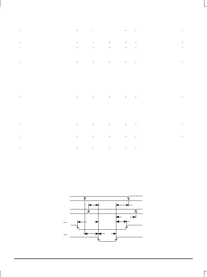
standard product. See Figure 1. |
Write Enable Setup Prior to Chip Select |
tCSW |
0 |
Ð |
|
|
Address Setup Prior to Chip Select |
tCSA |
0 |
Ð |
|
|
Data Hold Time After Chip Select |
tCHD |
1.0 |
Ð |
|
|
Write Enable Hold Time After Chip Select |
tCHW |
0 |
Ð |
|
|
Address Hold Time After Chip Select |
tCHA |
2.0 |
Ð |
|
|
Chip Select Minimum Pulse Width |
tCS |
4.0 |
Ð |
|
|
Rise and Fall Time |
tr, tf |
|
|
ns |
Measured between 20% and 80% |
Address to Output |
|
0.6 |
2.5 |
|
points. |
CS to Output |
|
0.6 |
2.5 |
|
|
|
|
|
|
|
|
Capacitance |
|
|
|
pF |
Measured with a pulse technique. |
Input Capacitance |
Cin |
Ð |
6.0 |
|
|
Output Capacitance |
Cout |
Ð |
8.0 |
|
|
NOTES: 1. Test circuit characteristics: RT = 50 Ω, MC10H145. CL p5.0 pF (including jig and Stray Capacitance). Delay should be derated 30 ps/pF for capacitive loads up to 50 pF.
2.The maximum Address Access Time is guaranteed to be the worst-case bit in the memory.
3.For proper use of MECL in a system environment, consult MECL System Design Handbook.
FIGURE 1 Ð CHIP ENABLE STROBE MODE
A |
|
|
|
TCSD |
TCHA |
DIN |
|
TCHD |
|
|
|
WE |
TCSW |
TCHW |
|
|
|
TCSA |
TCS |
|
CS |
|
|
MOTOROLA |
2±234 |
MECL Data |
DL122 Ð Rev 6
 Loading...