


MC10H158MEL
MOTOROLA MC10H158MEL, MC10H158ML1, MC10H158ML2, MC10H158MR1, MC10H158L Datasheet
...
SEMICONDUCTOR TECHNICAL DATA
2–238
REV 5
Motorola, Inc. 1996
3/93
"
!
The MC10H158 is a quad two channel multiplexer with common input select.
A “high” level select enables input D00, D10, D20 and D30 and a “low” level
select enables input D01, D11, D21 and D31. This MECL 10H part is a
functional/pinout duplication of the standard MECL 10K family part, with 100%
improvement in propagation delay and no increase in power–supply current.
• Propagation Delay, 1.5 ns Typical
• Power Dissipation, 197 mW Typical
• Improved Noise Margin 150 mV (Over Operating Voltage and
Temperature Range)
• Voltage Compensated
• MECL 10K–Compatible
MAXIMUM RATINGS
Characteristic Symbol Rating Unit
Power Supply (VCC = 0) V
EE
–8.0 to 0 Vdc
Input Voltage (VCC = 0) V
I
0 to V
EE
Vdc
Output Current— Continuous
— Surge
I
out
50
100
mA
Operating Temperature Range T
A
0 to +75 °C
Storage Temperature Range— Plastic
— Ceramic
T
stg
–55 to +150
–55 to +165
°C
°C
ELECTRICAL CHARACTERISTICS (VEE = –5.2 V ±5%)
0° 25° 75°
Characteristic Symbol Min Max Min Max Min Max Unit
Power Supply Current I
E
— 53 — 48 — 53 mA
Input Current High
Pin 9
Pins 3–6 and 10–13
I
inH
——475
515——
295
320——
295
320
µA
Input Current Low I
inL
0.5 — 0.5 — 0.3 — µA
High Output Voltage V
OH
–1.02 –0.84 –0.98 –0.81 –0.92 –0.735 Vdc
Low Output Voltage V
OL
–1.95 –1.63 –1.95 –1.63 –1.95 –1.60 Vdc
High Input Voltage V
IH
–1.17 –0.84 –1.13 –0.81 –1.07 –0.735 Vdc
Low Input Voltage V
IL
–1.95 –1.48 –1.95 –1.48 –1.95 –1.45 Vdc
AC PARAMETERS
Propagation Delay
Data
Select
t
pd
0.5
1.0
1.9
2.9
0.5
1.0
1.9
2.9
0.5
1.0
2.0
2.9
ns
Rise Time t
r
0.7 2.2 0.7 2.2 0.7 2.2 ns
Fall Time t
f
0.7 2.2 0.7 2.2 0.7 2.2 ns
NOTE:
Each MECL 10H series circuit has been designed to meet the dc specifications shown in the test table,
after thermal equilibrium has been established. The circuit is in a test socket or mounted on a printed circuit
board and transverse air flow greater than 500 Iinear fpm is maintained. Outputs are terminated through
a 50–ohm resistor to –2.0 volts.
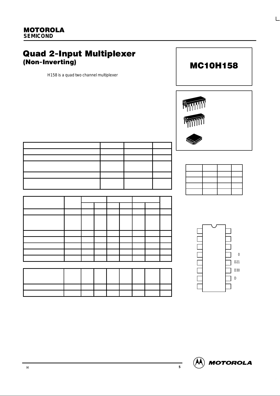
DIP
PIN ASSIGNMENT
Q0
Q1
D11
D10
D01
D00
NC
V
EE
V
CC
Q2
Q3
D20
D21
D30
D31
SELECT
16
15
14
13
12
11
10
9
1
2
3
4
5
6
7
8
TRUTH TABLE
Select D0 D1 Q
LLLX
LHHX
HXLL
HXHH
L SUFFIX
CERAMIC PACKAGE
CASE 620–10
P SUFFIX
PLASTIC PACKAGE
CASE 648–08
FN SUFFIX
PLCC
CASE 775–02
Pin assignment is for Dual–in–Line Package.
For PLCC pin assignment, see the Pin Conversion
T ables on page 6–11 of the Motorola MECL Data
Book (DL122/D).
MC10H158
2–239 MOTOROLAMECL Data
DL122 — Rev 6
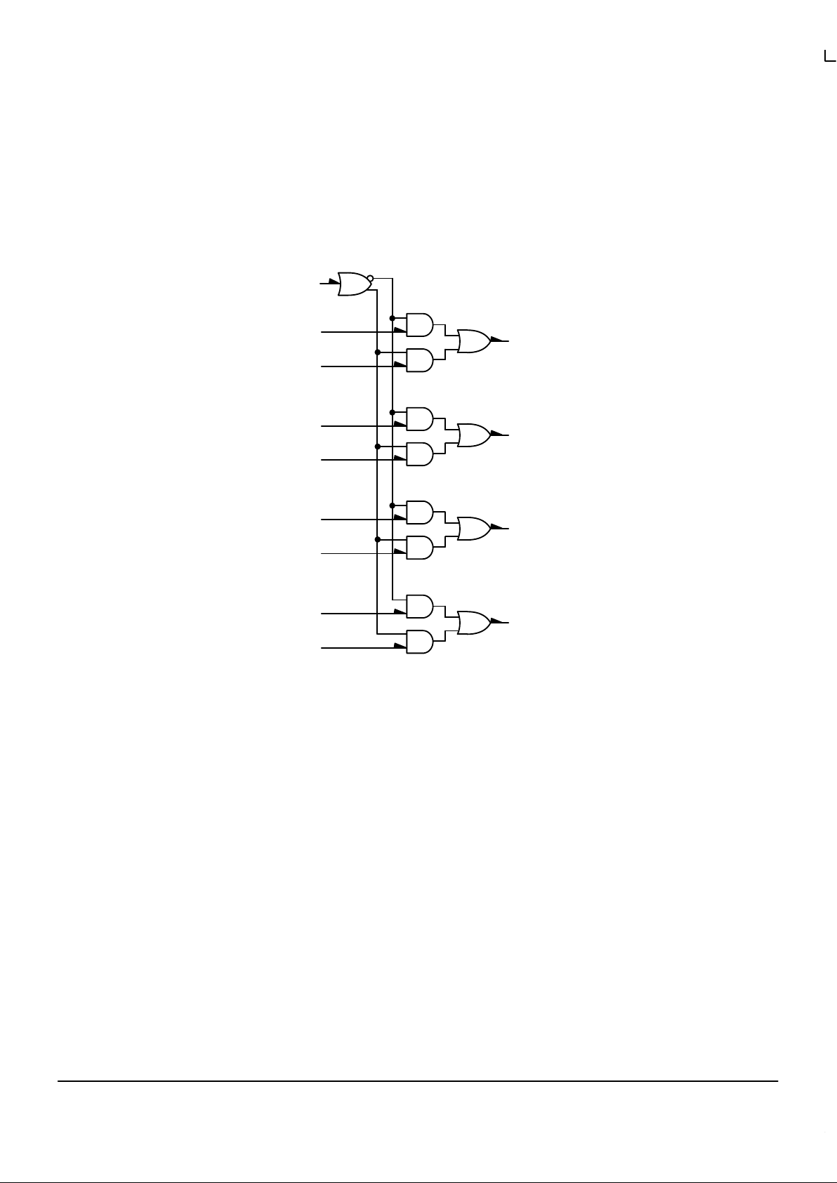
LOGIC DIAGRAM
VCC = PIN 16
VEE = PIN 8
SELECT 9
D0 1 5
D0 0 6
D1 1 3
D1 0 4
D2 1 12
D2 0 13
D3 1 10
D3 0 11
1 Q0
2 Q1
15 Q2
14 Q3
 Loading...