


MOTOROLA MC10H159ML1, MC10H159ML2, MC10H159MR1, MC10H159MEL, MC10H159L Datasheet
...
MOTOROLA
SEMICONDUCTOR TECHNICAL DATA
Quad 2-Input Multiplexer
(Inverting)
The MC10H159 is a quad 2±input multiplexer with enable. This MECL 10H part is a functional/pinout duplication of the standard MECL 10K family part, with 100% improvement in propagation delay and no increase in power±supply current.
•Propagation Delay, 1.5 ns Typical
•Power Dissipation, 218 mW Typical
•Improved Noise Margin 150 mV (Over Operating Voltage and Temperature Range)
•Voltage Compensated
•MECL 10K±Compatible
MAXIMUM RATINGS
Characteristic |
Symbol |
Rating |
Unit |
|
|
|
|
Power Supply (VCC = 0) |
VEE |
±8.0 to 0 |
Vdc |
Input Voltage (VCC = 0) |
VI |
0 to VEE |
Vdc |
Output Current Ð Continuous |
Iout |
50 |
mA |
Ð Surge |
|
100 |
|
|
|
|
|
Operating Temperature Range |
TA |
0 to +75 |
°C |
Storage Temperature Range Ð Plastic |
Tstg |
±55 to +150 |
°C |
Ð Ceramic |
|
±55 to +165 |
°C |
|
|
|
|
ELECTRICAL CHARACTERISTICS (VEE = ±5.2 V ±5%) (See Note)
|
|
0° |
25° |
|
75° |
|
|||
|
|
|
|
|
|
|
|
|
|
Characteristic |
Symbol |
Min |
Max |
Min |
Max |
Min |
|
Max |
Unit |
|
|
|
|
|
|
|
|
|
|
Power Supply Current |
IE |
Ð |
58 |
Ð |
53 |
Ð |
|
58 |
mA |
Input Current High |
IinH |
|
|
|
|
|
|
|
μA |
Pin 9 |
|
Ð |
475 |
Ð |
295 |
Ð |
|
295 |
|
Pins 3±7 and 10±13 |
|
Ð |
515 |
Ð |
320 |
Ð |
|
320 |
|
|
|
|
|
|
|
|
|
|
|
Input Current Low |
IinL |
0.5 |
Ð |
0.5 |
Ð |
0.3 |
|
Ð |
μA |
High Output Voltage |
VOH |
±1.02 |
±0.84 |
±0.98 |
±0.81 |
±0.92 |
|
±0.735 |
Vdc |
Low Output Voltage |
VOL |
±1.95 |
±1.63 |
±1.95 |
±1.63 |
±1.95 |
|
±1.60 |
Vdc |
High Input Voltage |
VIH |
±1.17 |
±0.84 |
±1.13 |
±0.81 |
±1.07 |
|
±0.735 |
Vdc |
Low Input Voltage |
VIL |
±1.95 |
±1.48 |
±1.95 |
±1.48 |
±1.95 |
|
±1.45 |
Vdc |
AC PARAMETERS |
|
|
|
|
|
|
|
|
|
|
|
|
|
|
|
|
|
|
|
Propagation Delay |
tpd |
|
|
|
|
|
|
|
ns |
Data |
|
0.5 |
2.2 |
0.5 |
2.2 |
0.5 |
|
2.2 |
|
Select |
|
1.0 |
3.2 |
1.0 |
3.2 |
1.0 |
|
3.2 |
|
Enable |
|
1.0 |
3.2 |
1.0 |
3.2 |
1.0 |
|
3.2 |
|
|
|
|
|
|
|
|
|
|
|
Rise Time |
tr |
0.5 |
2.2 |
0.5 |
2.2 |
0.5 |
|
2.2 |
ns |
Fall Time |
tf |
0.5 |
2.2 |
0.5 |
2.2 |
0.5 |
|
2.2 |
ns |
NOTE:
Each MECL 10H series circuit has been designed to meet the dc specifications shown in the test table, after thermal equilibrium has been established. The circuit is in a test socket or mounted on a printed circuit board and transverse air flow greater than 500 Iinear fpm is maintained. Outputs are terminated through a 50±ohm resistor to ±2.0 volts.
MC10H159
L SUFFIX
CERAMIC PACKAGE
CASE 620±10
P SUFFIX
PLASTIC PACKAGE
CASE 648±08
FN SUFFIX
PLCC
CASE 775±02
TRUTH TABLE
|
|
|
|
|
|
|
|
Enable |
Select |
D0 |
D1 |
Q |
|
|
|
|
|
|
|
|
|
L |
L |
X |
L |
H |
|
|
|
|
|
|
|
|
|
L |
L |
X |
H |
L |
|
|
L |
H |
L |
X |
H |
|
|
L |
H |
H |
X |
L |
|
|
H |
X |
X |
X |
L |
|
|
|
|
|
|
|
|
DIP
PIN ASSIGNMENT
|
|
|
|
|
|
|
|
|
|
|
|
Q0 |
|
1 |
|
16 |
|
|
VCC |
||
|
|
|
|
|
||||||
|
|
|
|
|
|
|
|
|
|
|
|
Q1 |
|
2 |
|
15 |
|
|
Q2 |
||
|
|
|
|
|
||||||
|
|
|
|
|
|
|
|
|
|
|
D11 |
|
3 |
|
14 |
|
|
Q3 |
|||
|
|
|
|
|||||||
D10 |
|
4 |
|
13 |
|
|
D20 |
|||
|
|
|
|
|||||||
D01 |
|
5 |
|
12 |
|
|
D21 |
|||
|
|
|
|
|||||||
D00 |
|
6 |
|
11 |
|
|
D30 |
|||
|
|
|
|
|||||||
|
|
|
|
|
|
|
|
|
D31 |
|
ENABLE |
|
7 |
|
10 |
|
|
||||
|
|
|
|
|||||||
VEE |
|
8 |
|
9 |
|
|
SELECT |
|||
|
|
|
|
|||||||
|
|
|
|
|
|
|
|
|
|
|
Pin assignment is for Dual±in±Line Package. For PLCC pin assignment, see the Pin Conversion Tables on page 6±11 of the Motorola MECL Data Book (DL122/D).
3/93
Motorola, Inc. 1996 |
2±242 |
REV 5 |
MC10H159
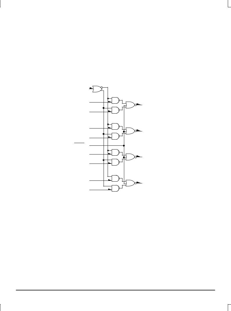
APPLICATION INFORMATION
The MC10H159 is a quad two channel multiplexer with enable. It incorporates common enable and common data select inputs. The select input determines which data inputs are enabled. A high (H) level enables data
inputs D0 0, D1 0, D2 0, and D3 0. A low (L) level enables data inputs D0 1, D1 1, D2 1, and D3 1. Any change on the data inputs will be reflected at the outputs while the enable is low. Input levels are inverted at the output.
LOGIC DIAGRAM
SELECT 9
D0 1 5
1 Q0
D0 0 6
D1 1 3
2 Q1
D1 0 4
ENABLE 7
D2 1 12
15 Q2
D2 0 13
D3 1 10
14 Q3
D3 0 11
VCC PIN 16
VEE PIN 8
MECL Data |
2±243 |
MOTOROLA |
DL122 Ð Rev 6 |
|
|
 Loading...