Motorola MC100LVEL17DWR2, MC100LVEL17, MC100LVEL17DW, MC100EL17DWR2, MC100EL17DW Datasheet

MOTOROLA
SEMICONDUCTOR TECHNICAL DATA
Low Voltage Quad
Differential Receiver
The MC100LVEL17 is a low-voltage, quad differential receiver. The device is functionally equivalent to the E116 device with the capability of operation from either a ±3.3V or +3.3V supply voltage. The MC100EL17 is pin and functionally equivalent to the MC100LVEL17, but is specified for operation at the standard 100E ECL voltage supply.
The LVEL17 provides a VBB output for either single-ended use or as a DC bias for AC coupling to the device. The VBB pin should be used only as a bias for the LVEL17 as its current sink/source capability is limited. Whenever used, the VBB pin should be bypassed to ground via a 0.01μf capacitor.
Under open input conditions, the D input will be biased at VCC/2 and the D input will be pulled down to VEE. This operation will force the Q output LOW and ensure stability.
•325ps Propagation Delay
•High Bandwidth Output Transitions
•>2000V ESD Protection
•Operates from ±3.3/±4.5V (or +3.3/+5.0V) Supply
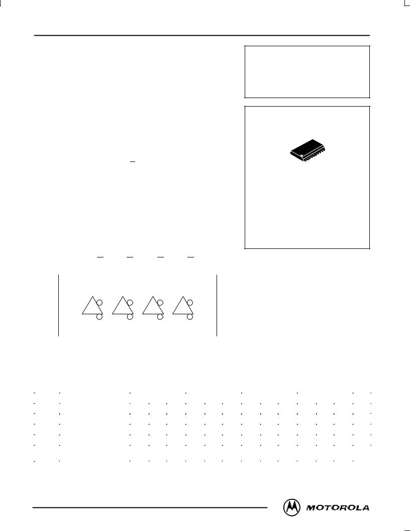
Logic Diagram and Pinout: 20-Lead SOIC (Top View)
MC100LVEL17
MC100EL17
1
DW SUFFIX
PLASTIC SOIC PACKAGE
CASE 751D-04
|
VCC |
Q0 |
Q0 |
|
Q1 |
Q1 |
Q2 |
Q2 |
Q3 |
Q3 |
VEE |
|||||||||||||||||
|
20 |
|
19 |
|
18 |
|
17 |
|
16 |
|
15 |
|
14 |
|
13 |
|
12 |
|
11 |
|
||||||||
|
|
|
|
|
|
|
|
|
|
|
|
|
|
|
|
|
|
|
|
|
|
|
|
|
|
|
|
|
|
|
|
|
|
|
|
|
|
|
|
|
|
|
|
|
|
|
|
|
|
|
|
|
|
|
|
|
|
|
|
|
|
|
|
|
|
|
|
|
|
|
|
|
|
|
|
|
|
|
|
|
|
|
|
|
|
|
|
|
|
|
|
|
|
|
|
|
|
|
|
|
|
|
|
|
|
|
|
|
|
|
|
|
|
|
|
|
|
|
|
|
|
|
|
|
|
|
|
|
|
|
1 |
|
2 |
|
3 |
|
|
4 |
|
|
5 |
|
|
6 |
|
7 |
|
|
8 |
|
9 |
|
|
10 |
|
||||||||||
|
|
|
|
|
|
|
|
|
|
|
|
|
|
|
|
|
|
|
|
|
|
|
|
|
|
|
|
|
|
|
|
|
|
|
|
|
VCC |
D0 |
|
D0 |
|
D1 |
D1 |
D2 |
D2 |
D3 |
|
D3 |
VBB |
|
|||||||||||||||||||||
PIN NAMES
Pins |
Function |
|
|
Dn |
Data Inputs |
Qn |
Data Outputs |
VBB |
Reference Voltage Output |
MC100LVEL17
DC CHARACTERISTICS (VEE = ±3.0V to ±3.8V; VCC = GND) Note 1
|
|
|
|
|
±40°C |
|
|
0°C |
|
|
25°C |
|
|
85°C |
|
|
|
|
|
|
|
|
|
|
|
|
|
|
|
|
|
|
|
Symbol |
Characteristic |
|
|
Min |
Typ |
Max |
Min |
Typ |
Max |
Min |
Typ |
Max |
Min |
Typ |
Max |
Unit |
|
|
|
|
|
|
|
|
|
|
|
|
|
|
|
|
|
IEE |
Power Supply Current |
|
|
|
26 |
31 |
|
26 |
31 |
|
26 |
31 |
|
27 |
33 |
mA |
VBB |
Output Reference Voltage |
±1.38 |
|
±1.26 |
±1.38 |
|
±1.26 |
±1.38 |
|
±1.26 |
±1.38 |
|
±1.26 |
V |
||
IIH |
Input HIGH Current |
|
|
|
|
150 |
|
|
150 |
|
|
150 |
|
|
150 |
μA |
IINL |
Input LOW Current |
Dn |
|
0.5 |
|
|
0.5 |
|
|
0.5 |
|
|
0.5 |
|
|
μA |
Dn |
|
|
|
|
|
|
|
|
||||||||
|
|
±300 |
|
|
±300 |
|
|
±300 |
|
|
±300 |
|
|
|
||
|
|
|
|
|
|
|
|
|
|
|
|
|
|
|
|
|
1. All other DC characteristics are the same as Standard 100K ECL.
4/95
Motorola, Inc. 1996 |
REV 2 |
 Loading...