


MC100LVEL38DWR2
Motorola MC100LVEL38DWR2, MC100LVEL38, MC100LVEL38DW, MC100EL38DW, MC100EL38DWR2 Datasheet
...
SEMICONDUCTOR TECHNICAL DATA
4–1
REV 1
Motorola, Inc. 1996
10/94
÷
÷
The MC100LVEL38 is a low skew ÷2, ÷4/6 clock generation chip
designed explicitly for low skew clock generation applications. The
MC100EL38 is pin and functionally equivalent to the MC100LVEL38 but
is specified for operation at the standard 100K ECL voltage supply. The
internal dividers are synchronous to each other, therefore, the common
output edges are all precisely aligned. The device can be driven by either
a differential or single-ended LVECL or, if positive power supplies are
used, LVPECL input signal. In addition, by using the VBB output, a
sinusoidal source can be AC coupled into the device (see Interfacing
section of the ECLinPS Data Book DL140/D). If a single-ended input is
to be used, the VBB output should be connected to the CLK
input and
bypassed to ground via a 0.01µF capacitor. The VBB output is designed to
act as the switching reference for the input of the LVEL38 under
single-ended input conditions, as a result, this pin can only source/sink up
to 0.5mA of current.
The common enable (EN
) is synchronous so that the internal dividers
will only be enabled/disabled when the internal clock is already in the
LOW state. This avoids any chance of generating a runt clock pulse on
the internal clock when the device is enabled/disabled as can happen
with an asynchronous control. An internal runt pulse could lead to losing
synchronization between the internal divider stages. The internal enable
flip-flop is clocked on the falling edge of the input clock, therefore, all
associated specification limits are referenced to the negative edge of the
clock input.
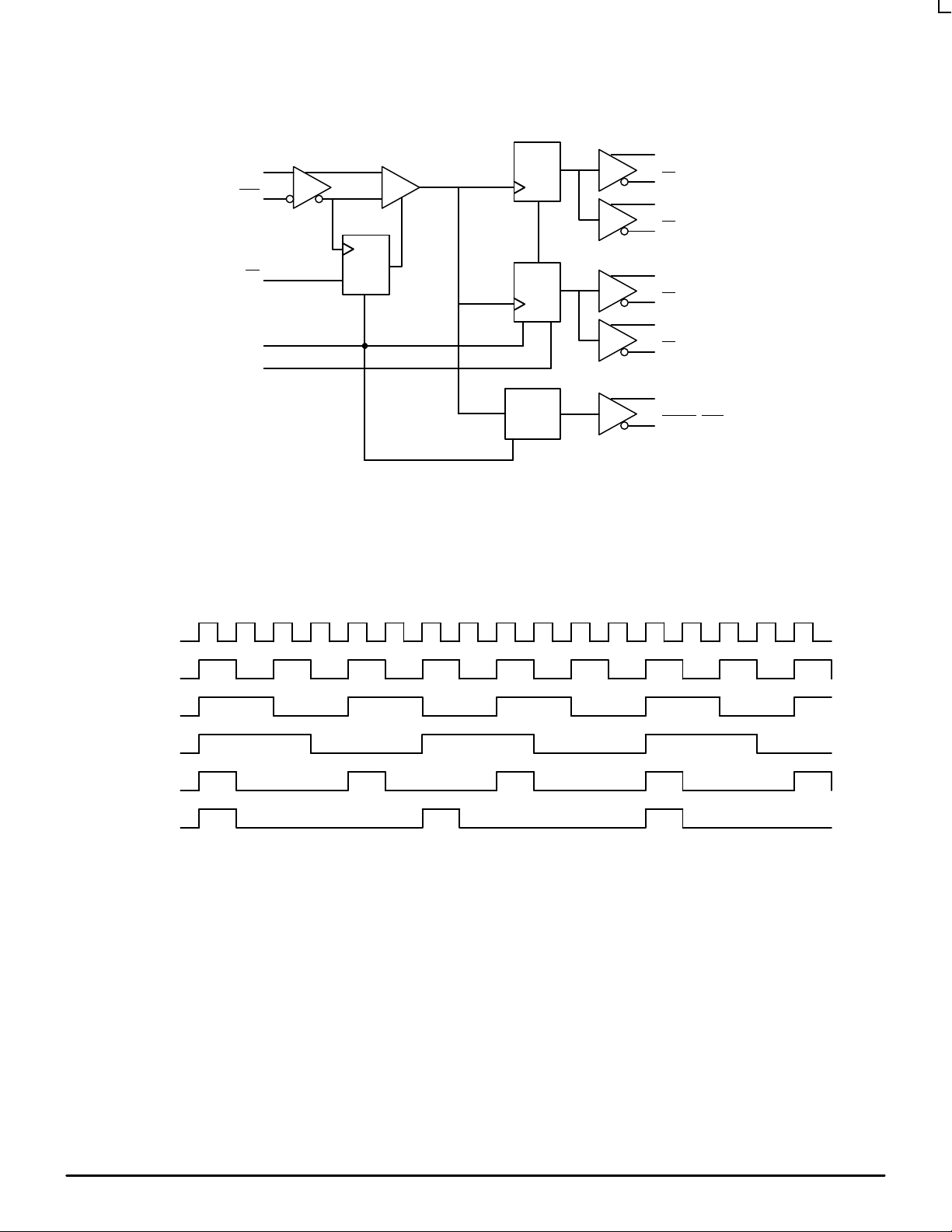
The Phase_Out output will go HIGH for one clock cycle whenever the
÷2 and the ÷4/6 outputs are both transitioning from a LOW to a HIGH.
This output allows for clock synchronization within the system.
Upon startup, the internal flip-flops will attain a random state; therefore,
for systems which utilize multiple LVEL38s, the master reset (MR) input
must be asserted to ensure synchronization. For systems which only use
one LVEL38, the MR pin need not be exercised as the internal divider
design ensures synchronization between the ÷2 and the ÷4/6 outputs of a
single device.
• 50ps Output-to-Output Skew
• Synchronous Enable/Disable
• Master Reset for Synchronization
• 75kΩ Internal Input Pulldown Resistors
• >1500V ESD Protection
• Low Voltage V
EE
Range of –3.0 to –3.8V
CLK
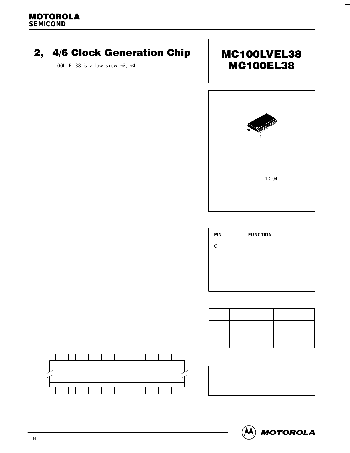
Pinout: 20-Lead SOIC (Top View)
CLK MR V
CC
1718 16 15 14 13 12
43
5 6 7 8 9
Q0
11
10
Q1 Q1 Q2 Q2 Q3 Q3 V
EE
EN
1920
21
VCCQ0
Phase_Out
Phase_Out
DIV_SEL V
BB
V
CC
DW SUFFIX
PLASTIC SOIC PACKAGE
CASE 751D-04
1
20
PIN FUNCTION
CLK Diff Clock Inputs
EN
Sync Enable
MR Master Reset
V
BB
Reference Output
Q0, Q
1
Diff ÷2 Outputs
Q2, Q
3
Diff ÷4/6 Outputs
DIVSEL Frequency Select Input
Phase_Out Phase Sync Signal
PIN DESCRIPTION
CLK
Z
ZZ
X
EN
L
H
X
MR
L
L
H
FUNCTION
Divide
Hold Q
0–3
Reset Q
0–3
FUNCTION TABLE
Z = Low-to-High Transition
ZZ = High-to-Low Transition
DIVSEL Q2, Q3 OUTPUTS
0 Divide by 4
1 Divide by 6
MC100LVEL38 MC100EL38
MOTOROLA ECLinPS and ECLinPS Lite
DL140 — Rev 3
4–2
Phase
Out
Logic
CLK
CLK
EN
MR
DIVSEL
÷
2
Q0
Q0
Q1
Q1
÷
4/6
Q2
Q2
Q3
Q3
PHASE_OUT
PHASE_OUT
LOGIC DIAGRAM
R
R
R
R
CLK
Q (
÷
2)
Q (
÷
4)
Q (
÷
6)
Phase_Out (
÷
4)
Phase_Out (
÷
6)
Figure 1. Timing Diagrams
 Loading...