Motorola MC100LVEL11D, MC100LVEL11DR2, MC100LVEL11 Datasheet

MOTOROLA
SEMICONDUCTOR TECHNICAL DATA
Low Voltage |
MC100LVEL11 |
|
1:2 Differential Fanout Buffer |
||
|
||
|
|
The MC100LVEL11 is a differential 1:2 fanout buffer. The device is functionally similar to the E111 device but with higher performance capabilities. Having within-device skews and output transition times significantly improved over the E111, the LVEL11 is ideally suited for those applications which require the ultimate in AC performance.
The differential inputs of the LVEL11 employ clamping circuitry to maintain stability under open input conditions. If the inputs are left open (pulled to VEE) the Q outputs will go LOW.
•330ps Propagation Delay
•5ps Skew Between Outputs
•High Bandwidth Output Transitions
•75kΩ Internal Input Pulldown Resistors
•>2000V ESD Protection
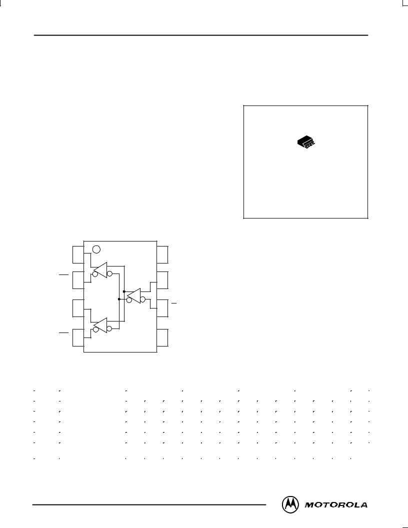
LOGIC DIAGRAM AND PINOUT ASSIGNMENT
Q0 |
1 |
8 |
VCC |
Q0 |
2 |
7 |
D |
Q1 |
3 |
6 |
D |
Q1 |
4 |
5 |
VEE |
8 

1
D SUFFIX
PLASTIC SOIC PACKAGE
CASE 751-05
PIN DESCRIPTION
PIN |
FUNCTION |
|
|
D |
Data Inputs |
Q0, Q1 |
Data Outputs |
|
|
DC CHARACTERISTICS (VEE = VEE(min) to VEE(max); VCC = GND)
|
|
|
|
|
±40°C |
|
|
0°C |
|
|
25°C |
|
|
85°C |
|
|
|
|
|
|
|
|
|
|
|
|
|
|
|
|
|
|
|
Symbol |
Characteristic |
Min |
Typ |
Max |
Min |
Typ |
Max |
Min |
Typ |
Max |
Min |
Typ |
Max |
Unit |
||
|
|
|
|
|
|
|
|
|
|
|
|
|
|
|
|
|
IEE |
Power Supply Current |
|
24 |
28 |
|
24 |
28 |
|
24 |
28 |
|
25 |
30 |
mA |
||
VEE |
Power Supply Voltage |
±3.0 |
±3.3 |
±3.8 |
±3.0 |
±3.3 |
±3.8 |
±3.0 |
±3.3 |
±3.8 |
±3.0 |
±3.3 |
±3.8 |
V |
||
IIH |
Input HIGH Current |
|
|
150 |
|
|
150 |
|
|
150 |
|
|
150 |
μA |
||
IIL |
Input LOW Current |
Dn |
|
0.5 |
|
|
0.5 |
|
|
0.5 |
|
|
0.5 |
|
|
μA |
Dn |
|
|
|
|
|
|
|
|
||||||||
|
|
±600 |
|
|
±600 |
|
|
±600 |
|
|
±600 |
|
|
|
||
|
|
|
|
|
|
|
|
|
|
|
|
|
|
|
|
|
1/96
Motorola, Inc. 1996 |
REV 0 |
 Loading...