


AD5627R
Table of contents
 Loading...
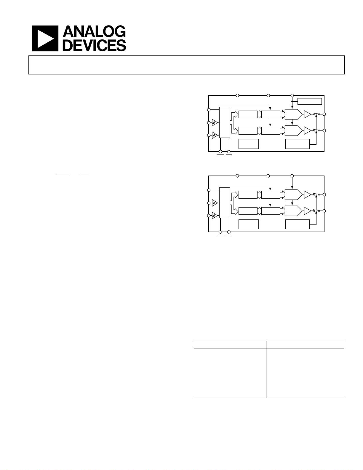
Dual, 12-/14-/16-Bit nanoDACs® with
A
V
V
/
A
V
V
AD5627R/AD5647R/AD5667R, AD5627/AD5667
5 ppm/°C On-Chip Reference, I
FEATURES
Low power, smallest pin-compatible, dual nanoDACs
AD5627R/AD5647R/AD5667R
12-/14-/16-bit
On-chip 1.25 V/2.5 V, 5 ppm/°C reference
AD5627/AD5667
12-/16-bit
External reference only
3 mm x 3 mm LFCSP and 10-lead MSOP
2.7 V to 5.5 V power supply
Guaranteed monotonic by design
Power-on reset to zero scale
Per channel power-down
Hardware
2
I
C-compatible serial interface supports standard (100 kHz),
LDAC
and
CLR
functions
fast (400 kHz), and high speed (3.4 MHz) modes
APPLICATIONS
Process control
Data acquisition systems
Portable battery-powered instruments
Digital gain and offset adjustment
Programmable voltage and current sources
Programmable attenuators
FUNCTIONAL BLOCK DIAGRAMS
AD5627R/AD5647R/AD5667R
DDR
SCL
SDA
DDR
SCL
SDA
LOGIC
INTERFACE
LDAC CLR
Figure 1. AD5627R/AD5647R/AD5667R
AD5627/AD5667
LOGIC
INTERFACE
LDAC CLR
DD
INPUT
REGISTER
INPUT
REGISTER
POWER-ON
RESET
DD
INPUT
REGISTER
INPUT
REGISTER
POWER-ON
RESET
GND
DAC
REGISTER
DAC
REGISTER
GND
DAC
REGISTER
DAC
REGISTER
Figure 2. AD5627/AD5667
2C®
Interface
V
REFIN
REFOUT
1.25V/2.5V REF
BUFFER
STRING
DAC A
BUFFER
STRING
DAC B
POWER-DOWN
LOGIC
REFIN
BUFFER
STRING
DAC A
BUFFER
STRING
DAC B
POWER-DOWN
LOGIC
V
A
OUT
V
B
OUT
06342-001
V
A
OUT
V
B
OUT
06342-002
GENERAL DESCRIPTION
The AD5627R/AD5647R/AD5667R, AD5627/AD5667
members of the nanoDAC family are low power, dual, 12-, 14-,
16-bit buffered voltage-out DACs with/without on-chip
reference. All devices operate from a single 2.7 V to 5.5 V
supply, are guaranteed monotonic by design, and have an I
compatible serial interface.
The AD5627R/AD5647R/AD5667R have an on-chip reference.
The AD56x7RBCPZ have a 1.25 V, 5 ppm/°C reference, giving a
full-scale output range of 2.5 V; the AD56x7RBRMZ have a
2.5 V, 5 ppm/°C reference, giving a full-scale output range of 5
V. The on-chip reference is off at power-up, allowing the use of
an external reference. The internal reference is enabled via a
software write. The AD5667 and AD5627 require an external
reference voltage to set the output range of the DAC.
The AD56x7R/AD56x7 incorporate a power-on reset circuit
that ensures the DAC output powers up to 0 V, and remains
there until a valid write takes place. The part contains a perchannel power-down feature that reduces the current
consumption of the device to 480 nA at 5 V and provides
Rev. 0
Information furnished by Analog Devices is believed to be accurate and reliable. However, no
responsibility is assumed by Anal og Devices for its use, nor for any infringements of patents or ot her
rights of third parties that may result from its use. Specifications subject to change without notice. No
license is granted by implication or otherwise under any patent or patent rights of Analog Devices.
Trademarks and registered trademarks are the property of their respective owners.
2
C-
software-selectable output loads while in power-down mode.
The low power consumption of this part in normal operation
makes it ideally suited to portable battery-operated equipment.
The on-chip precision output amplifier enables rail-to-rail
output swing.
2
The AD56x7R/AD56x7 use a 2-wire I
C-compatible serial
interface that operates in standard (100 kHz), fast (400 kHz),
and high speed (3.4 MHz) modes.
Table 1. Related Devices
Part No. Description
AD5663 2.7 V to 5.5 V, dual 16-bit DAC,
AD5623R/AD5643R/AD5663R 2.7 V to 5.5 V, dual 12-, 14-, 16-bit
AD5625R/AD5645R/AD5665R,
AD5625/AD5665
One Technology Way, P.O. Box 9106, Norwood, MA 02062-9106, U.S.A.
Tel: 781.329.4700 www.analog.com
Fax: 781.461.3113 ©2007 Analog Devices, Inc. All rights reserved.
external reference, SPI® interface
DACs, internal reference,
SPI interface
2.7 V to 5.5 V, quad 12-, 14-, 16-bit
DACs, with/without internal
reference, I
2
C interface

AD5627R/AD5647R/AD5667R, AD5627/AD5667
TABLE OF CONTENTS
Features.............................................................................................. 1
Applications....................................................................................... 1
Functional Block Diagrams............................................................. 1
General Description......................................................................... 1
Revision History ...............................................................................2
Specifications..................................................................................... 3
AC Characteristics........................................................................ 5
2
I
C Timing Specifications............................................................ 6
Absolute Maximum Ratings............................................................ 8
ESD Caution.................................................................................. 8
Pin Configuration and Function Descriptions............................. 9
Typical Performance Characteristics ........................................... 10
Terminology .................................................................................... 18
Theory of Operation ......................................................................20
D/A Section................................................................................. 20
Resistor String............................................................................. 20
Output Amplifier........................................................................ 20
Internal reference........................................................................20
External reference....................................................................... 20
Serial Interface............................................................................ 21
Write Operation.......................................................................... 21
Read Operation........................................................................... 21
High Speed Mode....................................................................... 21
Input Shift Register .................................................................... 23
Multiple Byte Operation............................................................ 23
Broadcast Mode.......................................................................... 23
LDAC
Function .......................................................................... 23
Power-Down Modes .................................................................. 25
Power-On Reset and Software Reset ....................................... 26
Clear Pin (
Internal Reference Setup (R Versions) .................................... 26
Application Information................................................................ 27
Using a Reference as a Power Supply for the
AD56x7R/AD56x7..................................................................... 27
Bipolar Operation Using the AD56x7R/AD56x7 .................. 27
Power Supply Bypassing and Grounding................................ 27
Outline Dimensions....................................................................... 28
Ordering Guide .......................................................................... 29
CLR
).......................................................................... 26
REVISION HISTORY
1/07—Revision 0: Initial Version
Rev. 0 | Page 2 of 32

AD5627R/AD5647R/AD5667R, AD5627/AD5667
SPECIFICATIONS
VDD = 2.7 V to 5.5 V; RL = 2 kΩ to GND; CL = 200 pF to GND; V
= VDD; all specifications T
REFIN
MIN
to T
, unless otherwise noted.
MAX
Table 2.
Parameter Min Typ Max Unit Conditions/Comments
STATIC PERFORMANCE
2
1
AD5667R/AD5667
Resolution 16 Bits
Relative Accuracy ±8 ±12 LSB
Differential Nonlinearity ±1 LSB Guaranteed monotonic by design
AD5647R
Resolution 14 Bits
Relative Accuracy ±2 ±4 LSB
Differential Nonlinearity ±0.5 LSB Guaranteed monotonic by design
AD5627R/AD5627
Resolution 12 Bits
Relative Accuracy ±0.5 ±1 LSB
Differential Nonlinearity ±0.25 LSB Guaranteed monotonic by design
Zero-Code Error 2 10 mV All 0s loaded to DAC register
Offset Error ±1 ±10 mV
Full-Scale Error −0.1 ±1 % of FSR All 1s loaded to DAC register
Gain Error ±1.5 % of FSR
Zero-Code Error Drift ±2 µV/°C
Gain Temperature Coefficient ±2.5 ppm Of FSR/°C
DC Power Supply Rejection Ratio −100 dB DAC code = midscale ; VDD = 5 V ± 10%
DC Crosstalk (External Reference) 15 µV
Due to full-scale output change,
= 2 kΩ to GND or 2 kΩ to V
R
L
DD
10 µV/mA Due to load current change
8 µV Due to powering down (per channel)
DC Crosstalk (Internal Reference) 25 µV
Due to full-scale output change,
R
= 2 kΩ to GND or 2 kΩ to V
L
DD
20 µV/mA Due to load current change
10 µV Due to powering down (per channel)
OUTPUT CHARACTERISTICS
3
Output Voltage Range 0 VDD V
Capacitive Load Stability 2 nF RL = ∞
10 nF RL = 2 kΩ
DC Output Impedance 0.5 Ω
Short-Circuit Current 30 mA VDD = 5 V
Power-Up Time 4 µs Coming out of power-down mode; VDD = 5 V
REFERENCE INPUTS
Reference Current 110 130 µA V
= VDD = 5.5 V
REF
Reference Input Range 0.75 VDD V
Reference Input Impedance 50 kΩ
REFERENCE OUTPUT
(LFCSP_WD PACKAGE)
Output Voltage 1.247 1.253 V At ambient
Reference TC
3
±10 ppm/°C
Output Impedance 7.5 kΩ
REFERENCE OUTPUT (MSOP PACKAGE)
Output Voltage 2.495 2.505 V At ambient
Reference TC
3
±5 ±10 ppm/°C
Output Impedance 7.5 kΩ
Rev. 0 | Page 3 of 32

AD5627R/AD5647R/AD5667R, AD5627/AD5667
Parameter Min Typ Max Unit Conditions/Comments
LOGIC INPUTS (ADDR, CLR, LDAC)
3
1
IIN, Input Current ±1 µA
V
, Input Low Voltage 0.15 × VDD V
INL
V
, Input High Voltage 0.85 × VDD V
INH
CIN, Pin Capacitance 2 pF ADDR
20 pF
V
, Input Hysteresis 0.1 × VDD V
HYST
CLR, LDAC
LOGIC INPUTS (SDA, SCL)
IIN, Input Current ±1 µA
V
, Input Low Voltage 0.3 × VDD V
INL
V
, Input High Voltage 0.7 × VDD V
INH
CIN, Pin Capacitance 2 pF
V
, Input Hysteresis 0.1 × VDD V
HYST
LOGIC OUTPUTS (OPEN-DRAIN)
VOL, Output Low Voltage 0.4 V I
0.6 V I
= 3 mA
SINK
= 6 mA
SINK
Floating-State Leakage Current ±1 µA
Floating-State Output Capacitance 2 pF
POWER REQUIREMENTS
VDD 2.7 5.5 V
IDD (Normal Mode)
4
V
= VDD, VIL = GND
IH
VDD = 4.5 V to 5.5 V 0.4 0.5 mA Internal reference off
VDD = 2.7 V to 3.6 V 0.35 0.45 mA Internal reference off
VDD = 4.5 V to 5.5 V 0.95 1.15 mA Internal reference on
VDD = 2.7 V to 3.6 V 0.8 0.95 mA Internal reference on
IDD (All Power-Down Modes)
1
Temperature range: B grade: −40°C to +105°C.
2
Linearity calculated using a reduced code range: AD5567R/AD5667 (Code 512 to Code 65,024); AD5647R (Code 128 to Code 16,256); AD5627R/AD5627 (Code 32 to
Code 4064). Output unloaded.
3
Guaranteed by design and characterization, not production tested.
4
Interface inactive. All DACs active. DAC outputs unloaded.
5
All DACs powered down.
5
0.48 1 µA VIH = VDD, VIL = GND
Rev. 0 | Page 4 of 32

AD5627R/AD5647R/AD5667R, AD5627/AD5667
AC CHARACTERISTICS
VDD = 2.7 V to 5.5 V; RL = 2 kΩ to GND; CL = 200 pF to GND; V
= VDD; all specifications T
REFIN
MIN
to T
, unless otherwise noted.
MAX
1
Table 3.
Parameter
2
Min Typ Max Unit Conditions/Comments
3
Output Voltage Settling Time
AD5627R/AD5627 3 4.5 µs ¼ to ¾ scale settling to ±0.5 LSB
AD5647R 3.5 5 µs ¼ to ¾ scale settling to ±0.5 LSB
AD5667R/AD5667 4 7 µs ¼ to ¾ scale settling to ±2 LSB
Slew Rate 1.8 V/µs
Digital-to-Analog Glitch Impulse 15 nV-s 1 LSB change around major carry transition
Digital Feedthrough 0.1 nV-s
Reference Feedthrough −90 dB V
= 2 V ± 0.1 V p-p, frequency 10 Hz to 20 MHz
REF
Digital Crosstalk 0.1 nV-s
Analog Crosstalk 1 nV-s External reference
4 nV-s Internal reference
DAC-to-DAC Crosstalk 1 nV-s External reference
4 nV-s Internal reference
Multiplying Bandwidth 340 kHz V
Total Harmonic Distortion −80 dB V
= 2 V ± 0.1 V p-p
REF
= 2 V ± 0.1 V p-p, frequency = 10 kHz
REF
Output Noise Spectral Density 120 nV/√Hz DAC code = midscale, 1 kHz
100 nV/√Hz DAC code = midscale, 10 kHz
Output Noise 15 µV p-p 0.1 Hz to 10 Hz
1
Guaranteed by design and characterization, not production tested.
2
See the Terminology section.
3
Temperature range is −40°C to +105°C, typical @ 25°C.
Rev. 0 | Page 5 of 32

AD5627R/AD5647R/AD5667R, AD5627/AD5667
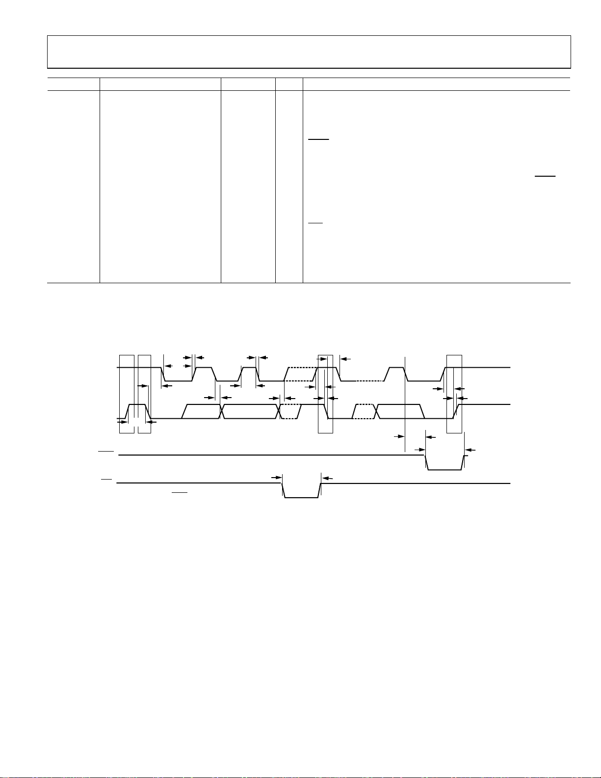
I2C TIMING SPECIFICATIONS
VDD = 2.7 V to 5.5 V; all specifications T
Table 4.
Parameter Conditions2 Min Max Unit Description
3
f
Standard mode 100 kHz Serial clock frequency
SCL
Fast mode 400 kHz
High speed mode, CB = 100 pF 3.4 MHz
High speed mode, CB = 400 pF 1.7 MHz
t1 Standard mode 4 s t
Fast mode 0.6 s
High speed mode, CB = 100 pF 60 ns
High speed mode, CB = 400 pF 120 ns
t2 Standard mode 4.7 s t
Fast mode 1.3 s
High speed mode, CB = 100 pF 160 ns
High speed mode, CB = 400 pF 320 ns
t3 Standard mode 250 ns t
Fast mode 100 ns
High speed mode 10 ns
t4 Standard mode 0 3.45 s t
Fast mode 0 0.9 s
High speed mode, CB = 100 pF 0 70 ns
High speed mode, CB = 400 pF 0 150 ns
t5 Standard mode 4.7 s t
Fast mode 0.6 s
High speed mode 160 ns
t6 Standard mode 4 s t
Fast mode 0.6 s
High speed mode 160 ns
t7 Standard mode 4.7 s t
Fast mode 1.3 s
t8 Standard mode 4 s t
Fast mode 0.6 s
High speed mode 160 ns
t9 Standard mode 1000 ns t
Fast mode 300 ns
High speed mode, CB = 100 pF 10 80 ns
High speed mode, CB = 400 pF 20 160 ns
t10 Standard mode 300 ns t
Fast mode 300 ns
High speed mode, CB = 100 pF 10 80 ns
High speed mode, CB = 400 pF 20 160 ns
t11 Standard mode 1000 ns t
Fast mode 300 ns
High speed mode, CB = 100 pF 10 40 ns
High speed mode, CB = 400 pF 20 80 ns
t
Standard mode 1000 ns
11A
Fast mode 300 ns
High speed mode, CB = 100 pF 10 80 ns
High speed mode, CB = 400 pF 20 160 ns
MIN
to T
, f
= 3.4 MHz, unless otherwise noted.1
MAX
SCL
, SCL high time
HIGH
, SCL low time
LOW
, data setup time
SU;DAT
, data hold time
HD;DAT
setup time for a repeated start condition
SU;STA,
, hold time (repeated) start condition
HD;STA
, bus free time between a stop and a start condition
BUF
, setup time for a stop condition
SU;STO
, rise time of SDA signal
RDA
, fall time of SDA signal
FDA
, rise time of SCL signal
RCL
, rise time of SCL signal after a repeated start condition and after
t
RCL1
an acknowledge bit
Rev. 0 | Page 6 of 32
AD5627R/AD5647R/AD5667R, AD5627/AD5667
Parameter Conditions2 Min Max Unit Description
t12 Standard mode 300 ns t
Fast mode 300 ns
High speed mode, CB = 100 pF 10 40 ns
High speed mode, CB = 400 pF 20 80 ns
t13 Standard mode 10 ns
Fast mode 10 ns
High speed mode 10 ns
t14 Standard mode 300 ns
Fast mode 300 ns
High speed mode 30 ns
t15 Standard mode 20 ns
Fast mode 20 ns
High speed mode 20 ns
4
t
Fast mode 0 50 ns Pulse width of spike suppressed
SP
High speed mode 0 10 ns
1
See Figure 3. High speed mode timing specification applies only to the AD5627RBRMZ-2/AD5627BRMZ-2REEL7 and AD5667RBRMZ-2/AD5667BRMZ-2REEL7.
2
CB refers to the capacitance on the bus line.
3
The SDA and SCL timing is measured with the input filters enabled. Switching off the input filters improves the transfer rate but has a negative effect on EMC behavior
of the part.
4
Input filtering on the SCL and SDA inputs suppresses noise spikes that are less than 50 ns for fast mode or 10 ns for high speed mode.
t
t
SCL
SDA
t
7
PS S P
2
t
6
11
t
4
t
12
t
1
t
3
, fall time of SCL signal
FCL
LDAC pulse width low
th
Falling edge of 9
SCL clock pulse of last byte of valid write to LDAC
falling edge
CLR pulse width low
t
6
t
5
t
10
t
8
t
14
t
9
LDAC*
CLR
*ASYNCHRONOUS LDAC UPDAT E MODE.
t
15
Figure 3. 2-Wire Serial Interface Timing Diagram
t
13
06342-003
Rev. 0 | Page 7 of 32
AD5627R/AD5647R/AD5667R, AD5627/AD5667
ABSOLUTE MAXIMUM RATINGS
TA = 25°C, unless otherwise noted.
Table 5.
Parameter Rating
VDD to GND −0.3 V to +7 V
V
to GND −0.3 V to VDD + 0.3 V
OUT
V
REFIN/VREFOUT
Digital Input Voltage to GND −0.3 V to VDD + 0.3 V
Operating Temperature Range, Industrial −40°C to +105°C
Storage Temperature Range −65°C to +150°C
Junction Temperature (TJ maximum) 150°C
Power Dissipation (TJ max − TA)/θJA
θJA Thermal Impedance
LFCSP_WD Package (4-Layer Board) 61°C/W
MSOP Package 150.4°C/W
Reflow Soldering Peak Temperature, Pb-Free 260°C ± 5°C
to GND −0.3 V to VDD + 0.3 V
Stresses above those listed under Absolute Maximum Ratings
may cause permanent damage to the device. This is a stress
rating only; functional operation of the device at these or any
other conditions above those indicated in the operational
section of this specification is not implied. Exposure to absolute
maximum rating conditions for extended periods may affect
device reliability.
ESD CAUTION
Rev. 0 | Page 8 of 32

AD5627R/AD5647R/AD5667R, AD5627/AD5667
PIN CONFIGURATION AND FUNCTION DESCRIPTIONS
1
V
A
OUT
V
OUT
LDAC
GND
CLR
AD5627/
2
B
AD5667
3
4
TOP VIEW
(Not to Scale)
5
EXPOSED PAD TIED TO GND
ON LFCSP PACKAGE.
Figure 4. AD5627/AD5667 Pin Configuration
10
V
REFIN
9
V
DD
8
SDA
7
SCL
6
ADDR
06342-101
1
V
A
OUT
V
OUT
GND
LDAC
CLR
AD5627R/
2
B
AD5647R/
3
AD5667R
4
TOP VIEW
(Not to Scal e)
5
EXPOSED PAD TIED TO GND
ON LFCSP PACKAGE.
10
V
REFIN/VREFOUT
9
V
DD
8
SDA
7
SCL
6
ADDR
06342-102
Figure 5. AD5627R/AD5647R/AD5667R Pin Configuration
Table 6. Pin Function Descriptions
Pin
Mnemonic Description
No.
1 V
2 V
A Analog Output Voltage from DAC A. The output amplifier has rail-to-rail operation.
OUT
B Analog Output Voltage from DAC B. The output amplifier has rail-to-rail operation.
OUT
3 GND Ground reference point for all circuitry on the part.
4
LDAC Pulsing this pin low allows any or all DAC registers to be updated if the inputs have new data. This allows
simultaneous updates of all DAC outputs. Alternatively, this pin can be tied permanently low.
5
CLR Asynchronous Clear Input. The CLR input is falling-edge sensitive. While CLR is low, all LDAC pulses are ignored.
CLR is activated, zero scale is loaded to all input and DAC registers. This clears the output to 0 V. The part exits
When
clear code mode on the falling edge of the 9th clock pulse of the last byte of valid write. If CLR is activated during a
write sequence, the write is aborted. If
CLR is activated during high speed mode the part will exit high speed mode.
6 ADDR Three-State Address Input. Sets the two least significant bits (Bit A1, Bit A0) of the 7-bit slave address.
7 SCL Serial Clock Line. This is used in conjunction with the SDA line to clock data into or out of the 24-bit input register.
8 SDA
Serial Data Line. This is used in conjunction with the SCL line to clock data into or out of the 24-bit input register. It is
a bidirectional, open-drain data line that should be pulled to the supply with an external pull-up resistor.
9 VDD
Power Supply Input. These parts can be operated from 2.7 V to 5.5 V, and the supply should be decoupled with a
10 F capacitor in parallel with a 0.1 F capacitor to GND.
10 V
REFIN/VREFOUT
The AD56x7R have a common pin for reference input and reference output. When using the internal reference, this is
the reference output pin. When using an external reference, this is the reference input pin. The default for this pin is
as a reference input. (The internal reference and reference output are only available on R suffix versions.) The AD56x7
has a reference input pin only.
Rev. 0 | Page 9 of 32
AD5627R/AD5647R/AD5667R, AD5627/AD5667
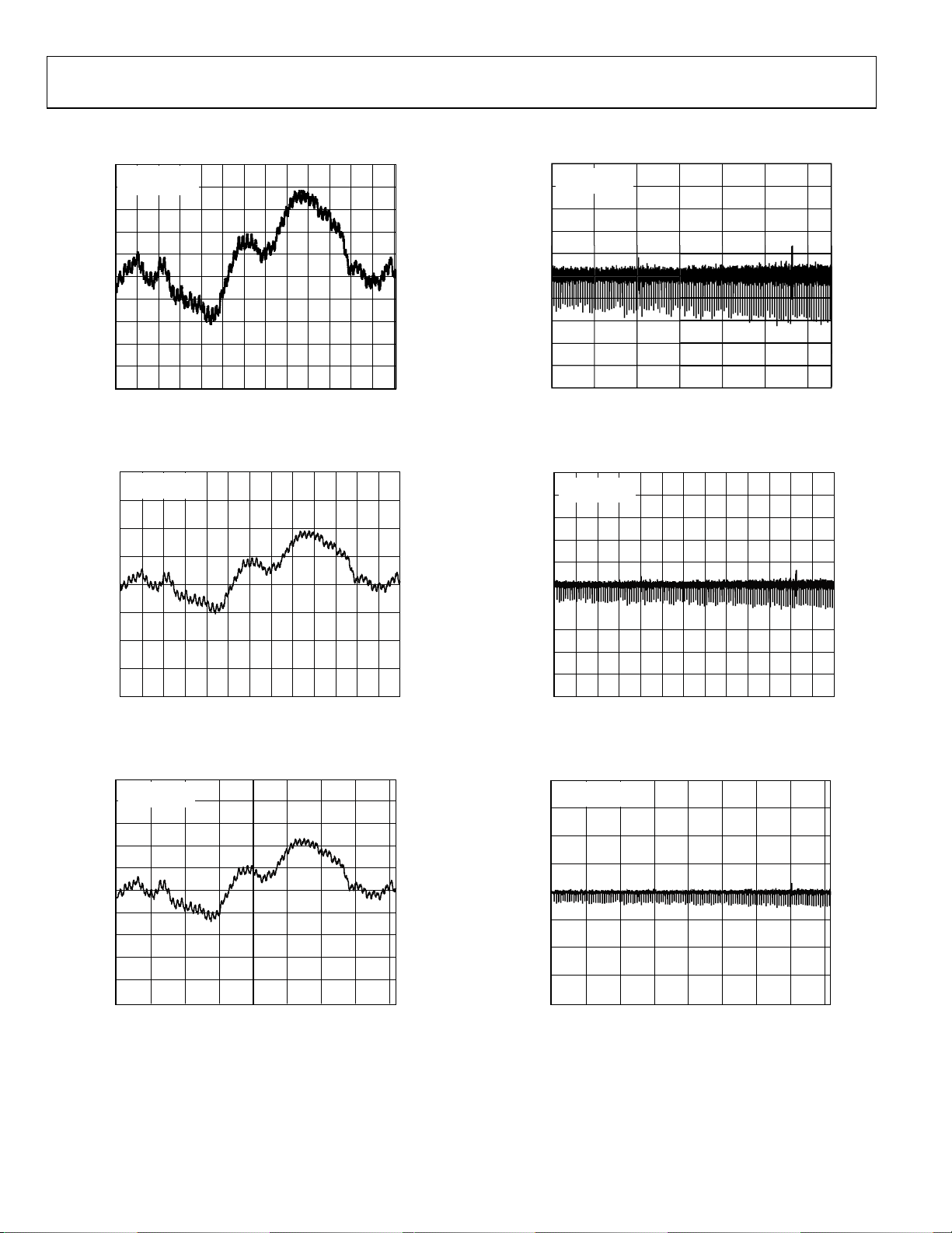
TYPICAL PERFORMANCE CHARACTERISTICS
10
VDD = V
T
8
6
4
2
0
–2
INL ERROR (LSB)
–4
–6
–8
–10
0 5k 10k 15k 20k 25k 30k 35k 40k 45k 50k 55k 60k 65k
= 25°C
A
REF
= 5V
CODE
Figure 6. AD5667 INL, External Reference
06342-005
1.0
VDD = V
T
0.8
0.6
0.4
0.2
0
–0.2
DNL ERROR (LSB)
–0.4
–0.6
–0.8
–1.0
0 10k 20k 30k 40k 50k 60k
= 25°C
A
REF
= 5V
CODE
Figure 9. AD5667 DNL, External Reference
6342-007
4
VDD = V
T
3
2
1
0
–1
INL ERROR (L SB)
–2
–3
–4
0 2500 5000 7500 10000 12500 15000
= 25°C
A
REF
= 5V
CODE
Figure 7. AD5647R INL, External Reference
1.0
VDD = V
T
0.8
0.6
0.4
0.2
0
–0.2
INL ERROR (L SB)
–0.4
–0.6
–0.8
–1.0
0 500 1000 1500 2000 2500 3000 3500 4000
= 25°C
A
REF
= 5V
CODE
Figure 8. AD5627 INL, External Reference
0.5
VDD = V
T
0.4
0.3
0.2
0.1
0
–0.1
DNL ERROR (LSB)
–0.2
–0.3
–0.4
–0.5
06342-006
0 2500 5000 7500 10000 12500 15000
= 25°C
A
REF
= 5V
CODE
6342-008
Figure 10. DNL AD5647R, External Reference
0.20
VDD = V
T
0.15
0.10
0.05
0
–0.05
DNL ERROR (LSB)
–0.10
–0.15
–0.20
06342-100
0 500 1000 1500 2000 2500 3000 3500 4000
= 25°C
A
REF
= 5V
CODE
6342-009
Figure 11. AD5627 DNL, External Reference
Rev. 0 | Page 10 of 32
Loading...