


a 2.5 V to 5.5 V, 500 A, 2-Wire Interface
Quad Voltage Output, 8-/10-/12-Bit DACs
|
AD5305/AD5315/AD5325* |
|
FEATURES |
GENERAL DESCRIPTION |
|
AD5305 |
The AD5305/AD5315/AD5325 are quad 8-, 10and 12-bit |
|
Four Buffered 8-Bit DACs in 10-Lead microSOIC |
buffered voltage output DACs in a 10-lead microSOIC package |
|
AD5315 |
that operate from a single 2.5 V to 5.5 V supply consuming |
|
Four Buffered 10-Bit DACs in 10-Lead microSOIC |
500 A at 3 V. Their on-chip output amplifiers allow rail-to-rail |
|
AD5325 |
output swing with a slew rate of 0.7 V/ s. A 2-wire serial inter- |
|
Four Buffered 12-Bit DACs in 10-Lead microSOIC |
face is used which operates at clock rates up to 400 kHz. This |
|
Low Power Operation: 500 A @ 3 V, 600 A @ 5 V |
interface is SMBus-compatible at VDD < 3.6 V. Multiple devices |
|
2-Wire (I2C®-Compatible) Serial Interface |
can be placed on the same bus. |
|
2.5 V to 5.5 V Power Supply |
The references for the four DACs are derived from one reference |
|
Guaranteed Monotonic By Design Over All Codes |
||
pin. The outputs of all DACs may be updated simultaneously |
||
Power-Down to 80 nA @ 3 V, 200 nA @ 5 V |
||
using the software LDAC function. The parts incorporate a |
||
Double-Buffered Input Logic |
||
power-on-reset circuit that ensures that the DAC outputs power |
||
Output Range: 0–VREF |
||
up to zero volts and remain there until a valid write takes place |
||
Power-On-Reset to Zero Volts |
||
to the device. There is also a software clear function which resets |
||
Simultaneous Update of Outputs (LDAC Function) |
||
all input and DAC registers to 0 V. The parts contain a power- |
||
Software Clear Facility |
||
down feature that reduces the current consumption of the devices |
||
Data Readback Facility |
||
to 200 nA @ 5 V (80 nA @ 3 V). |
||
On-Chip Rail-to-Rail Output Buffer Amplifiers |
||
The low power consumption of these parts in normal operation |
||
Temperature Range –40 C to +105 C |
||
makes them ideally suited to portable battery-operated equip- |
||
APPLICATIONS |
||
ment. The power consumption is 3 mW at 5 V, 1.5 mW at 3 V, |
||
Portable Battery-Powered Instruments |
reducing to 1 W in power-down mode. |
|
Digital Gain and Offset Adjustment |
|
|
Programmable Voltage and Current Sources |
|
|
Programmable Attenuators |
|
|
Industrial Process Control |
|
FUNCTIONAL BLOCK DIAGRAM
|
|
VDD |
|
REF IN |
|
|
|
LDAC |
|
|
|
|
|
|
|
INPUT |
DAC |
STRING |
BUFFER |
VOUTA |
|
|
REGISTER |
REGISTER |
DAC A |
|
|
SCL |
|
INPUT |
DAC |
STRING |
BUFFER |
VOUTB |
|
|
REGISTER |
REGISTER |
DAC B |
||
SDA |
INTERFACE |
|
|
|
|
|
LOGIC |
|
|
|
|
|
|
|
|
INPUT |
DAC |
STRING |
BUFFER |
VOUTC |
A0 |
|
REGISTER |
REGISTER |
DAC C |
||
|
|
|
|
|
|
|
|
|
INPUT |
DAC |
STRING |
BUFFER |
VOUTD |
|
|
REGISTER |
REGISTER |
|||
|
|
DAC D |
||||
|
|
|
|
|
|
|
|
POWER-ON |
|
|
|
POWER-DOWN |
|
|
AD5305/AD5315/AD5325 |
LOGIC |
|
|||
|
RESET |
|
|
|
|
|
|
|
|
GND |
|
|
|
*Protected by U.S. Patent No. 5,969,657; other patents pending. I2C is a registered trademark of Philips Corporation.
REV. B
Information furnished by Analog Devices is believed to be accurate and reliable. However, no responsibility is assumed by Analog Devices for its use, nor for any infringements of patents or other rights of third parties which may result from its use. No license is granted by implication or otherwise under any patent or patent rights of Analog Devices.
One Technology Way, P.O. Box 9106, Norwood, MA 02062-9106, U.S.A.
Tel: 781/329-4700 |
World Wide Web Site: http://www.analog.com |
Fax: 781/326-8703 |
© Analog Devices, Inc., 2000 |
AD5305/AD5315/AD5325–SPECIFICATIONS(VDD = 2.5 V to 5.5 V; VREF = 2 V; RL = 2 k to
GND; CL = 200 pF to GND; All specifications TMIN to TMAX unless otherwise noted.)
Parameter1 |
B Version2 |
|
|
|
|
Min |
Typ |
Max |
Unit |
Conditions/Comments |
|
DC PERFORMANCE3, 4 |
|
|
|
|
|
AD5305 |
|
|
|
|
|
Resolution |
|
8 |
|
Bits |
|
Relative Accuracy |
|
± 0.15 |
± 1 |
LSB |
|
Differential Nonlinearity |
|
± 0.02 |
± 0.25 |
LSB |
Guaranteed Monotonic by Design Over All Codes |
AD5315 |
|
|
|
|
|
Resolution |
|
10 |
|
Bits |
|
Relative Accuracy |
|
± 0.5 |
± 4 |
LSB |
|
Differential Nonlinearity |
|
± 0.05 |
± 0.5 |
LSB |
Guaranteed Monotonic by Design Over All Codes |
AD5325 |
|
|
|
|
|
Resolution |
|
12 |
|
Bits |
|
Relative Accuracy |
|
± 2 |
± 16 |
LSB |
|
Differential Nonlinearity |
|
± 0.2 |
± 1 |
LSB |
Guaranteed Monotonic by Design Over All Codes |
Offset Error |
|
± 0.4 |
± 3 |
% of FSR |
|
Gain Error |
|
± 0.15 |
± 1 |
% of FSR |
|
Lower Deadband |
|
20 |
60 |
mV |
Lower Deadband Exists Only If Offset Error Is Negative |
Offset Error Drift5 |
|
–12 |
|
ppm of FSR/°C |
|
Gain Error Drift5 |
|
–5 |
|
ppm of FSR/°C |
∆VDD = ± 10% |
Power Supply Rejection Ratio5 |
|
–60 |
|
dB |
|
DC Crosstalk5 |
|
200 |
|
µV |
RL = 2 k to GND or VDD |
DAC REFERENCE INPUTS5 |
|
|
|
|
|
VREF Input Range |
0.25 |
|
VDD |
V |
|
VREF Input Impedance |
37 |
45 |
|
kΩ |
Normal Operation |
|
|
>10 |
|
MΩ |
Power-Down Mode |
Reference Feedthrough |
|
–90 |
|
dB |
Frequency = 10 kHz |
OUTPUT CHARACTERISTICS5 |
|
|
|
|
|
Minimum Output Voltage6 |
|
0.001 |
|
V |
This is a measure of the minimum and maximum drive |
Maximum Output Voltage6 |
|
VDD – 0.001 |
|
V |
capability of the output amplifier. |
DC Output Impedance |
|
0.5 |
|
Ω |
|
Short Circuit Current |
|
25 |
|
mA |
VDD = 5 V |
|
|
16 |
|
mA |
VDD = 3 V |
Power-Up Time |
|
2.5 |
|
µs |
Coming Out of Power-Down Mode. VDD = 5 V |
|
|
5 |
|
µs |
Coming Out of Power-Down Mode. VDD = 3 V |
LOGIC INPUTS (A0)5 |
|
|
± 1 |
µA |
|
Input Current |
|
|
VDD = 5 V ± 10% |
||
VIL, Input Low Voltage |
|
|
0.8 |
V |
|
|
|
|
0.6 |
V |
VDD = 3 V ± 10% |
|
|
|
0.5 |
V |
VDD = 2.5 V |
VIH, Input High Voltage |
2.4 |
|
|
V |
VDD = 5 V ± 10% |
|
2.1 |
|
|
V |
VDD = 3 V ± 10% |
|
2.0 |
|
|
V |
VDD = 2.5 V |
Pin Capacitance |
|
3 |
|
pF |
|
LOGIC INPUTS (SCL, SDA)5 |
|
|
|
|
|
VIH, Input High Voltage |
0.7 VDD |
|
VDD + 0.3 |
V |
SMBus-Compatible at VDD < 3.6 V |
VIL, Input Low Voltage |
–0.3 |
|
0.3 VDD |
V |
SMBus-Compatible at VDD < 3.6 V |
IIN, Input Leakage Current |
|
|
± 1 |
µA |
|
VHYST, Input Hysteresis |
0.05 VDD |
|
|
V |
|
CIN, Input Capacitance |
|
8 |
|
pF |
|
Glitch Rejection |
|
|
50 |
ns |
Input filtering suppresses noise spikes of less than 50 ns. |
LOGIC OUTPUT (SDA)5 |
|
|
|
|
|
VOL, Output Low Voltage |
|
|
0.4 |
V |
ISINK = 3 mA |
|
|
|
0.6 |
V |
ISINK = 6 mA |
Three-State Leakage Current |
|
|
± 1 |
µA |
|
Three-State Output Capacitance |
|
8 |
|
pF |
|
POWER REQUIREMENTS |
|
|
|
|
|
VDD |
2.5 |
|
5.5 |
V |
|
IDD (Normal Mode)7 |
|
|
|
µA |
VIH = VDD and VIL = GND |
VDD = 4.5 V to 5.5 V |
|
600 |
900 |
|
|
VDD = 2.5 V to 3.6 V |
|
500 |
700 |
µA |
|
IDD (Power-Down Mode) |
|
|
|
|
VIH = VDD and VIL = GND, |
VDD = 4.5 V to 5.5 V |
|
0.2 |
1 |
µA |
IDD = 4 µA (Max) During “0” Readback on SDA |
VDD = 2.5 V to 3.6 V |
|
0.08 |
1 |
µA |
IDD = 1.5 µA (Max) During “0” Readback on SDA |
–2– |
REV. B |
AD5305/AD5315/AD5325
NOTES
1See Terminology.
2Temperature range: B Version: –40°C to +105°C; typical at 25°C. 3DC specifications tested with the outputs unloaded.
4Linearity is tested using a reduced code range: AD5305 (Code 8 to 248); AD5315 (Code 28 to 995); AD5325 (Code 115 to 3981). 5Guaranteed by design and characterization, not production tested.
6For the amplifier output to reach its minimum voltage, Offset Error must be negative; to reach its maximum voltage, VREF = VDD and “Offset plus Gain” Error must be positive. 7IDD specification is valid for all DAC codes. Interface inactive. All DACs active and excluding load currents.
Specifications subject to change without notice.
1 |
(VDD = 2.5 V to 5.5 V; RL = 2 k to GND; CL = 200 pF to GND; all specifications TMIN to TMAX unless |
||||||
AC CHARACTERISTICS |
otherwise noted.) |
|
|
|
|||
|
Parameter2 |
|
|
B Version3 |
|
|
|
|
|
Min |
Typ |
Max |
Unit |
Conditions/Comments |
|
|
Output Voltage Settling Time |
|
|
|
|
s |
VREF = VDD = 5 V |
|
AD5305 |
|
|
6 |
8 |
1/4 Scale to 3/4 Scale Change (40 Hex to C0 Hex) |
|
|
AD5315 |
|
|
7 |
9 |
s |
1/4 Scale to 3/4 Scale Change (100 Hex to 300 Hex) |
|
AD5325 |
|
|
8 |
10 |
s |
1/4 Scale to 3/4 Scale Change (400 Hex to C00 Hex) |
|
Slew Rate |
|
|
0.7 |
|
V/ s |
|
|
Major-Code Transition Glitch Energy |
|
12 |
|
nV-s |
1 LSB Change Around Major Carry |
|
|
Digital Feedthrough |
|
|
1 |
|
nV-s |
|
|
Digital Crosstalk |
|
|
1 |
|
nV-s |
|
|
DAC-to-DAC Crosstalk |
|
|
3 |
|
nV-s |
VREF = 2 V ± 0.1 V p-p |
|
Multiplying Bandwidth |
|
|
200 |
|
kHz |
|
|
Total Harmonic Distortion |
|
|
–70 |
|
dB |
VREF = 2.5 V ± 0.1 V p-p. Frequency = 10 kHz |
NOTES
1Guaranteed by design and characterization, not production tested.
2See Terminology.
3Temperature range: B Version: –40°C to +105°C; typical at 25°C.
Specifications subject to change without notice.
TIMING CHARACTERISTICS1, 2 (VDD = 2.5 V to 5.5 V. All specifications TMIN to TMAX unless otherwise noted)
|
Limit at TMIN, TMAX |
|
|
Parameter |
(B Version) |
Unit |
Conditions/Comments |
|
|
|
|
FSCL |
400 |
kHz max |
SCL Clock Frequency |
t1 |
2.5 |
s min |
SCL Cycle Time |
t2 |
0.6 |
s min |
tHIGH, SCL High Time |
t3 |
1.3 |
s min |
tLOW, SCL Low Time |
t4 |
0.6 |
s min |
tHD,STA, Start/Repeated Start Condition Hold Time |
t5 |
100 |
ns min |
tSU,DAT, Data Setup Time |
t63 |
0.9 |
s max |
tHD,DAT, Data Hold Time |
|
0 |
s min |
tHD,DAT, Data Hold Time |
t7 |
0.6 |
s min |
tSU,STA, Setup Time for Repeated Start |
t8 |
0.6 |
s min |
tSU,STO, Stop Condition Setup Time |
t9 |
1.3 |
s min |
tBUF, Bus Free Time Between a STOP and a START Condition |
t10 |
300 |
ns max |
tR, Rise Time of SCL and SDA when Receiving |
|
0 |
ns min |
tR, Rise Time of SCL and SDA when Receiving (CMOS-Compatible) |
t11 |
250 |
ns max |
tF, Fall Time of SDA when Transmitting |
|
0 |
ns min |
tF, Fall Time of SDA when Receiving (CMOS-Compatible) |
|
300 |
ns max |
tF, Fall Time of SCL and SDA when Receiving |
|
20 + 0.1CB3 |
ns min |
tF, Fall Time of SCL and SDA when Transmitting |
CB |
400 |
pF max |
Capacitive Load for Each Bus Line |
NOTES
1See Figure 1.
2Guaranteed by design and characterization, not production tested.
3CB is the total capacitance of one bus line in pF. tR and tF measured between 0.3 VDD and 0.7 VDD. Specifications subject to change without notice.
REV. B |
–3– |
AD5305/AD5315/AD5325
SDA
t9 |
t3 |
t10 |
t11 |
t4 |
SCL
|
|
|
|
|
|
|
|
|
|
|
|
|
|
|
|
|
|
|
|
t4 |
|
|
|
|
|
|
|
|
|
|
|
|
|
|
|
|
|
|
|
t6 |
|
t2 |
|
|
|
|
|
|
|
t1 |
|
|
|
t8 |
|
|
|
|
|
|
|
|
|
|
|||||||||||
START |
|
|
|
|
t5 |
|
t7 |
|
|
|
|
|
|
|
|
|
||
|
|
|
|
|
|
|
|
STOP |
||||||||||
|
|
|
|
|
REPEATED |
|||||||||||||
CONDITION |
|
|
|
|
|
|||||||||||||
|
|
|
|
|
|
|
|
START |
CONDITION |
|||||||||
CONDITION
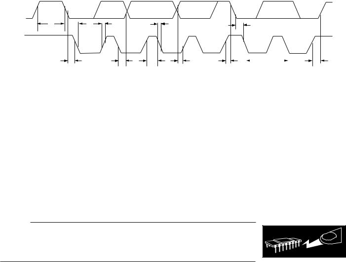
Figure 1. Two-Wire Serial Interface Timing Diagram
ABSOLUTE MAXIMUM RATINGS1, 2
(TA = 25°C unless otherwise noted)
VDD to GND . . . . . . . . . . . . . . . . |
. . . . . . . . . . –0.3 V to +7 V |
|
SCL, SDA to GND . . . . . . . . . . . |
. . . . .–0.3 V to VDD + 0.3 V |
|
A0 to GND . . . . . . . . . . . . . . . . . |
. . . . .–0.3 V to VDD + 0.3 |
V |
Reference Input Voltage to GND |
. . . . –0.3 V to VDD + 0.3 |
V |
VOUTA–D to GND . . . . . . . . . . . . |
. . . . –0.3 V to VDD + 0.3 V |
|
Operating Temperature Range |
–40°C to +105°C |
|
Industrial (B Version) . . . . . . . |
||
Storage Temperature Range . . . . |
. . . . . . . . –65°C to +150°C |
|
Junction Temperature (TJ max) . . |
. . . . . . . . . . . . . . . . . 150°C |
|
microSOIC Package |
(TJ max – TA)/θJA |
Power Dissipation . . . . . . . . . . . . . . . . . . |
|
θJA Thermal Impedance . . . . . . . . . . . . . . |
. . . . . . 206°C/W |
θJC Thermal Impedance . . . . . . . . . . . . . . . |
. . . . . . 44°C/W |
Reflow Soldering |
220 +5/–0°C |
Peak Temperature . . . . . . . . . . . . . . . . . . . |
|
Time at Peak Temperature . . . . . . . . . . . . |
10 sec to 40 sec |
NOTES
1Stresses above those listed under Absolute Maximum Ratings may cause permanent damage to the device. This is a stress rating only; and functional operation of the device at these or any other conditions above those listed in the operational sections of this specification is not implied. Exposure to absolute maximum rating conditions for extended periods may affect device reliability.
2Transient currents of up to 100 mA will not cause SCR latch-up.
CAUTION
ESD (electrostatic discharge) sensitive device. Electrostatic charges as high as 4000 V readily accumulate on the human body and test equipment and can discharge without detection. Although the AD5305/AD5315/AD5325 features proprietary ESD protection circuitry, permanent damage may occur on devices subjected to high-energy electrostatic discharges. Therefore, proper ESD precautions are recommended to avoid performance degradation or loss of functionality.
ORDERING GUIDE
WARNING!
ESD SENSITIVE DEVICE
|
Temperature |
Package |
Package |
Branding |
Model |
Range |
Description |
Option |
Information |
|
|
|
|
|
AD5305BRM |
–40°C to +105°C |
10-Lead microSOIC |
RM-10 |
DEB |
AD5315BRM |
–40°C to +105°C |
10-Lead microSOIC |
RM-10 |
DFB |
AD5325BRM |
–40°C to +105°C |
10-Lead microSOIC |
RM-10 |
DGB |
|
|
|
|
|
–4– |
REV. B |

AD5305/AD5315/AD5325
PIN CONFIGURATION
VDD |
|
|
|
|
|
A0 |
1 |
|
|
|
10 |
||
VOUTA |
|
AD5305/ |
|
SCL |
||
2 |
9 |
|||||
VOUTB |
|
AD5315/ |
|
SDA |
||
3 |
AD5325 |
8 |
||||
VOUTC |
|
TOP VIEW |
|
GND |
||
4 |
7 |
|||||
REFIN |
|
(Not to Scale) |
|
|
||
5 |
|
|
|
6 |
VOUTD |
|
|
|
|
|
|
|
|
|
|
PIN FUNCTION DESCRIPTIONS |
|
|
|
Pin |
|
|
No. |
Mnemonic |
Function |
|
|
|
1 |
VDD |
Power Supply Input. These parts can be operated from 2.5 V to 5.5 V and the supply should be |
|
|
decoupled to GND. |
2 |
VOUTA |
Buffered Analog Output Voltage from DAC A. The output amplifier has rail-to-rail operation. |
3 |
VOUTB |
Buffered Analog Output Voltage from DAC B. The output amplifier has rail-to-rail operation. |
4 |
VOUTC |
Buffered Analog Output Voltage from DAC C. The output amplifier has rail-to-rail operation. |
5 |
REFIN |
Reference Input Pin for All Four DACs. It has an input range from 0.25 V to VDD. |
6 |
VOUTD |
Buffered analog output voltage from DAC D. The output amplifier has rail-to-rail operation. |
7 |
GND |
Ground Reference Point for All Circuitry on the Part. |
8 |
SDA |
Serial Data Line. This is used in conjunction with the SCL line to clock data into or out of the 16-bit |
|
|
input shift register. It is a bidirectional open-drain data line that should be pulled to the supply with |
|
|
an external pull-up resistor. |
9 |
SCL |
Serial Clock Line. This is used in conjunction with the SDA line to clock data into or out of the 16-bit |
|
|
input shift register. Clock rates of up to 400 kbit/s can be accommodated in the 2-wire interface. |
10 |
A0 |
Address Input. Sets the least significant bit of the 7-bit slave address. |
|
|
|
TERMINOLOGY RELATIVE ACCURACY
For the DAC, relative accuracy or integral nonlinearity (INL) is a measure of the maximum deviation, in LSBs, from a straight line passing through the endpoints of the DAC transfer function. Typical INL versus Code plots can be seen in Figures 4, 5, and 6.
DIFFERENTIAL NONLINEARITY
OFFSET ERROR DRIFT
This is a measure of the change in offset error with changes in temperature. It is expressed in (ppm of full-scale range)/°C.
GAIN ERROR DRIFT
This is a measure of the change in gain error with changes in temperature. It is expressed in (ppm of full-scale range)/°C.
Differential Nonlinearity (DNL) is the difference between the measured change and the ideal 1 LSB change between any two adjacent codes. A specified differential nonlinearity of ±1 LSB maximum ensures monotonicity. This DAC is guaranteed monotonic by design. Typical DNL versus Code plots can be seen in Figures 7, 8, and 9.
POWER-SUPPLY REJECTION RATIO (PSRR)
This indicates how the output of the DAC is affected by changes in the supply voltage. PSRR is the ratio of the change
in VOUT to a change in VDD for full-scale output of the DAC. It is measured in dBs. VREF is held at 2 V and VDD is varied ±10%.
DC CROSSTALK
OFFSET ERROR
This is a measure of the offset error of the DAC and the output amplifier. It is expressed as a percentage of the full-scale range.
GAIN ERROR
This is a measure of the span error of the DAC. It is the deviation in slope of the actual DAC transfer characteristic from the ideal expressed as a percentage of the full-scale range.
This is the dc change in the output level of one DAC at midscale in response to a full-scale code change (all 0s to all 1s and vice versa) and output change of another DAC. It is expressed in V.
REFERENCE FEEDTHROUGH
This is the ratio of the amplitude of the signal at the DAC output to the reference input when the DAC output is not being updated. It is expressed in dBs.
REV. B |
–5– |
AD5305/AD5315/AD5325
MAJOR-CODE TRANSITION GLITCH ENERGY
Major-code transition glitch energy is the energy of the impulse injected into the analog output when the code in the DAC register changes state. It is normally specified as the area of the glitch in nV-secs and is measured when the digital code is changed by 1 LSB at the major carry transition (011 . . . 11 to 100 . . . 00 or 100 . . . 00 to 011 . . . 11).
DIGITAL FEEDTHROUGH
Digital feedthrough is a measure of the impulse injected into the analog output of the DAC from the digital input pins of the device when the DAC output is not being updated. It is specified in nV-secs and is measured with a worst-case change on the digital input pins, e.g., from all 0s to all 1s or vice versa.
DIGITAL CROSSTALK
This is the glitch impulse transferred to the output of one DAC at midscale in response to a full-scale code change (all 0s to all 1s and vice versa) in the input register of another DAC. It is expressed in nV-secs.
DAC-TO-DAC CROSSTALK
This is the glitch impulse transferred to the output of one DAC due to a digital code change and subsequent output change of another DAC. This includes both digital and analog crosstalk. It
is measured by loading one of the DACs with a full-scale code change (all 0s to all 1s and vice versa) with the LDAC bit set low
and monitoring the output of another DAC. The energy of the glitch is expressed in nV-secs.
MULTIPLYING BANDWIDTH
The amplifiers within the DAC have a finite bandwidth. The multiplying bandwidth is a measure of this. A sine wave on the reference (with full-scale code loaded to the DAC) appears on the output. The multiplying bandwidth is the frequency at which the output amplitude falls to 3 dB below the input.
TOTAL HARMONIC DISTORTION
This is the difference between an ideal sine wave and its attenuated version using the DAC. The sine wave is used as the reference for the DAC and the THD is a measure of the harmonics present on the DAC output. It is measured in dBs.
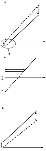
|
GAIN ERROR |
|
PLUS |
|
OFFSET ERROR |
OUTPUT |
IDEAL |
VOLTAGE |
|
|
ACTUAL |
NEGATIVE |
|
OFFSET |
DAC CODE |
ERROR |
|
DEADBAND CODES
AMPLIFIER  FOOTROOM
(1mV)
NEGATIVE
OFFSET
ERROR
Figure 2. Transfer Function with Negative Offset
|
GAIN ERROR |
|
PLUS |
ACTUAL |
OFFSET ERROR |
OUTPUT |
|
VOLTAGE |
|
IDEAL |
|
POSITIVE |
|
OFFSET |
|
DAC CODE |
|
Figure 3. Transfer Function with Positive Offset
–6– |
REV. B |
 Loading...