


AD630SE-883B
Analog Devices AD630SE-883B, AD630SD-883B, AD630SD, AD630SCHIPS, AD630S Datasheet
...
REV. D
Information furnished by Analog Devices is believed to be accurate and
reliable. However, no responsibility is assumed by Analog Devices for its
use, nor for any infringements of patents or other rights of third parties that
may result from its use. No license is granted by implication or otherwise
under any patent or patent rights of Analog Devices.
a
AD630
One Technology Way, P.O. Box 9106, Norwood, MA 02062-9106, U.S.A.
Tel: 781/329-4700 www.analog.com
Fax: 781/326-8703 © Analog Devices, Inc., 2001
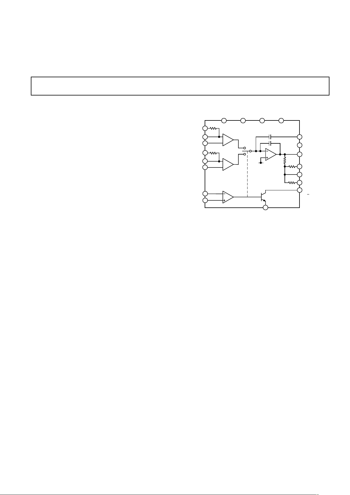
Balanced Modulator/Demodulator
FUNCTIONAL BLOCK DIAGRAM
CM OFF
ADJ
CM OFF
ADJ
DIFF OFF
ADJ
DIFF OFF
ADJ
6
34
5
2.5k⍀
AMP A
2.5k⍀
AMP B
–V
10k⍀
10k⍀
17
5k⍀
8
9
10
COMP
19
18
1
15
7
16
14
13
11
12
RINA
CHA+
CHA–
R
IN
B
CHB+
CHB–
SEL B
SEL A
2
20
COMP
+V
S
V
OUT
R
B
R
F
R
A
CHANNEL
STATUS
B/A
–V
S
AD630
A
B
PRODUCT DESCRIPTION
The AD630 is a high precision balanced modulator which combines a flexible commutating architecture with the accuracy and
temperature stability afforded by laser wafer trimmed thin-film
resistors. Its signal processing applications include balanced
modulation and demodulation, synchronous detection, phase
detection, quadrature detection, phase sensitive detection,
lock-in amplification and square wave multiplication. A network
of on-board applications resistors provides precision closed loop
gains of ± 1 and ± 2 with 0.05% accuracy (AD630B). These
resistors may also be used to accurately configure multiplexer
gains of +1, +2, +3 or +4. Alternatively, external feedback may
be employed allowing the designer to implement his own high
gain or complex switched feedback topologies.
The AD630 may be thought of as a precision op amp with two
independent differential input stages and a precision comparator
which is used to select the active front end. The rapid response
time of this comparator coupled with the high slew rate and fast
settling of the linear amplifiers minimize switching distortion. In
addition, the AD630 has extremely low crosstalk between channels of –100 dB @ 10 kHz.
The AD630 is intended for use in precision signal processing
and instrumentation applications requiring wide dynamic range.
When used as a synchronous demodulator in a lock-in amplifier
configuration, it can recover a small signal from 100 dB of interfering noise (see lock-in amplifier application). Although optimized
for operation up to 1 kHz, the circuit is useful at frequencies up
to several hundred kilohertz.
Other features of the AD630 include pin programmable frequency
compensation, optional input bias current compensation resistors, common-mode and differential-offset voltage adjustment,
and a channel status output which indicates which of the two
differential inputs is active. This device is now available to
Standard Military Drawing (DESC) numbers 5962-8980701RA
and 5962-89807012A.
PRODUCT HIGHLIGHTS
1. The configuration of the AD630 makes it ideal for signal
processing applications such as: balanced modulation and
demodulation, lock-in amplification, phase detection, and
square wave multiplication.
2. The application flexibility of the AD630 makes it the best
choice for many applications requiring precisely fixed gain,
switched gain, multiplexing, integrating-switching functions,
and high-speed precision amplification.
3. The 100 dB dynamic range of the AD630 exceeds that of any
hybrid or IC balanced modulator/demodulator and is comparable to that of costly signal processing instruments.
4. The op-amp format of the AD630 ensures easy implementation of high gain or complex switched feedback functions.
The application resistors facilitate the implementation of
most common applications with no additional parts.
5. The AD630 can be used as a two channel multiplexer with
gains of +1, +2, +3, or +4. The channel separation of
100 dB @ 10 kHz approaches the limit which is achievable
with an empty IC package.
6. The AD630 has pin-strappable frequency compensation (no
external capacitor required) for stable operation at unity gain
without sacrificing dynamic performance at higher gains.
7. Laser trimming of comparator and amplifying channel offsets
eliminates the need for external nulling in most cases.
FEATURES
Recovers Signal from +100 dB Noise
2 MHz Channel Bandwidth
45 V/s Slew Rate
–120 dB Crosstalk @ 1 kHz
Pin Programmable Closed Loop Gains of ⴞ1 and ⴞ2
0.05% Closed Loop Gain Accuracy and Match
100 V Channel Offset Voltage (AD630BD)
350 kHz Full Power Bandwidth
Chips Available

REV. D
–2–
AD630–SPECIFICATIONS
(@ 25ⴗC and ⴞVS = ⴞ15 V unless otherwise noted.)
Model AD630J/A AD630K/B AD630S
Min Typ Max Min Typ Max Min Typ Max Unit
GAIN
Open Loop Gain 90 110 100 120 90 110 dB
± 1, ± 2 Closed Loop Gain Error 0.1 0.05 0.1 %
Closed Loop Gain Match 0.1 0.05 0.1 %
Closed Loop Gain Drift 2 2 2 ppm/°C
CHANNEL INPUTS
VIN Operational Limit
1
(–VS + 4 V) to (+VS – 1 V) (–VS + 4 V) to (+VS – 1 V) (–VS + 4 V) to (+VS – 1 V) Volts
Input Offset Voltage 500 100 500 µV
Input Offset Voltage
T
MIN
to T
MAX
800 160 1000 µV
Input Bias Current 100 300 100 300 100 300 nA
Input Offset Current 10 50 10 50 10 50 nA
Channel Separation @ 10 kHz 100 100 100 dB
COMPARATOR
V
IN
Operational Limit
1
(–VS + 3 V) to (+VS – 1.5 V) (–VS + 3 V) to (+VS – 1.5 V) (–VS + 3 V) to (+VS – 1.3 V) Volts
Switching Window ± 1.5 ± 1.5 ± 1.5 mV
Switching Window
T
MIN
to T
MAX
± 2.0 ± 2.0 ± 2.5 mV
Input Bias Current 100 300 100 300 100 300 nA
Response Time (–5 mV to +5 mV Step) 200 200 200 ns
Channel Status
I
SINK
@ VOL = –VS + 0.4 V
2
1.6 1.6 1.6 mA
Pull-Up Voltage (–VS + 33 V) (–VS + 33 V) (–VS + 33 V) Volts
DYNAMIC PERFORMANCE
Unity Gain Bandwidth 2 2 2 MHz
Slew Rate
3
45 45 45 V/µs
Settling Time to 0.1% (20 V Step) 3 3 3 µs
OPERATING CHARACTERISTICS
Common-Mode Rejection 85 105 90 110 90 110 dB
Power Supply Rejection 90 110 90 110 90 110 dB
Supply Voltage Range ± 5 ± 16.5 ± 5 ± 16.5 ± 5 ± 16.5 Volts
Supply Current 4 5 4 5 4 5 mA
OUTPUT VOLTAGE, @ RL = 2 kΩ
T
MIN
to T
MAX
± 10 ± 10 ± 10 Volts
Output Short Circuit Current 25 25 25 mA
TEMPERATURE RANGES
Rated Performance–N Package 0 70 0 70 N/A °C
Rated Performance–D Package –25 +85 –25 +85 –55 +125 °C
NOTES
1
If one terminal of each differential channel or comparator input is kept within these limits the other terminal may be taken to the positive supply.
2
I
SINK
@ VOL = (–VS + 1) volt is typically 4 mA.
3
Pin 12 Open. Slew rate with Pins 12 and 13 shorted is typically 35 V/µs.
Specifications subject to change without notice.

REV. D
AD630
–3–
ABSOLUTE MAXIMUM RATINGS
Supply Voltage . . . . . . . . . . . . . . . . . . . . . . . . . . . . . . . . ± 18 V
Internal Power Dissipation . . . . . . . . . . . . . . . . . . . . 600 mW
Output Short Circuit to Ground . . . . . . . . . . . . . . . Indefinite
Storage Temperature, Ceramic Package . . . –65°C to +150°C
Storage Temperature, Plastic Package . . . . . –55°C to +125°C
Lead Temperature Range (Soldering, 10 sec) . . . . . . . . 300° C
Max Junction Temperature . . . . . . . . . . . . . . . . . . . . . . 150°C
PIN CONFIGURATIONS
20-Lead DIP (D-20 and N-20), 20-Lead SOIC (R-20)
14
13
12
11
17
16
15
20
19
18
10
9
8
1
2
3
4
7
6
5
TOP VIEW
(Not to Scale)
AD630
RINA
R
IN
B
CH B+
CH B–
CH A–
CH A+
DIFF OFF ADJ
DIFF OFF ADJ
R
B
R
F
R
A
CM OFF ADJ
CM OFF ADJ
–V
S
SEL B
SEL A
+V
S
COMP
V
OUT
CHANNEL STATUS B/A
20-Contact LCC (E-20A)
20 19123
18
14
15
16
17
4
5
6
7
8
910111213
TOP VIEW
(Not to Scale)
AD630
DIFF OFF ADJ
CM OFF ADJ
CM OFF ADJ
CHANNEL STATUS B/A
–V
S
CH B+
R
IN
B
R
A
R
F
R
B
DIFF
OFF ADJ
CH A+
R
IN
A
CH A–
CH B–
SEL B
SEL A
+V
S
COMP
V
OUT
ORDERING GUIDE
Model Temperature Ranges Package Description Package Option
AD630JN 0°C to 70°C Plastic DIP N-20
AD630KN 0°C to 70°C Plastic DIP N-20
AD630AR –25°C to +85°C SOIC R-20
AD630AR-REEL –25°C to +85°C 13" Tape and Reel R-20
AD630AD –25°C to +85°C Side Brazed DIP D-20
AD630BD –25°C to +85°C Side Brazed DIP D-20
AD630SD –55°C to +125°C Side Brazed DIP D-20
AD630SD/883B –55°C to +125°C Side Brazed DIP D-20
5962-8980701RA –55°C to +125°C Side Brazed DIP D-20
AD630SE/883B –55°C to +125°C LCC E-20A
5962-89807012A –55°C to +125°C LCC E-20A
AD630JCHIPS 0°C to 70°C Chip
AD630SCHIPS –55°C to +125°C Chip
THERMAL CHARACTERISTICS
JC
JA
20-Lead Plastic DIP (N) 24°C/W 61°C/W
20-Lead Ceramic DIP (D) 35°C/W 120°C/W
20-Lead Leadless Chip Carrier (E) 35°C/W 120°C/W
20-Lead SOIC (R-20) 38°C/W 75°C/W
CHIP METALIZATION AND PINOUT
Dimensions shown in inches and (mm).
Contact factory for latest dimensions.
CHIP AVAILABILITY
The AD630 is available in laser trimmed, passivated chip
form. The figure shows the AD630 metalization pattern, bonding pads and dimensions. AD630 chips are available; consult
factory for details.
CAUTION
ESD (electrostatic discharge) sensitive device. Electrostatic charges as high as 4000 V readily
accumulate on the human body and test equipment and can discharge without detection. Although
the AD630 features proprietary ESD protection circuitry, permanent damage may occur on devices
subjected to high-energy electrostatic discharges. Therefore, proper ESD precautions are
recommended to avoid performance degradation or loss of functionality.
WARNING!
ESD SENSITIVE DEVICE

REV. D
AD630
–4–
REV. D
10
15
5
1
10
100 1k 10k 100k 1M
RESISTIVE LOAD – ⍀
CL = 100pF
f = 1kHz
CAP IN
5k⍀
V
O
100pF
R
L
V
i
5k⍀
OUTPUT VOLTAGE – ⴞV
TPC 2. Output Voltage vs. Resistive
Load
INPUT VOLTAGE – V
DV
O
dt
– V/s
60
0
–60
–5 –3
4
–2 –1
1
40
20
–40
–20
–4
023 5
UNCOMPENSATED
COMPENSATED
TPC 5.
dV
dt
O
vs. Input Voltage
10
18
5
0 5 10 15
SUPPLY VOLTAGE – ⴞV
OUTPUT VOLTAGE – ⴞV
15
5k⍀
100pF
V
i
5k⍀
2k⍀
V
O
f = 1kHz
C
L
= 100pF
TPC 3. Output Voltage Swing vs.
Supply Voltage
FREQUENCY – Hz
120
60
0
1M100
100
80
20
40
10 1k 100k10k
UNCOMPENSATED
10M
0
45
90
OPEN LOOP GAIN – dB
135
180
COMPENSATED
OPEN LOOP PHASE – Degrees
TPC 6. Gain and Phase vs. Frequency
FREQUENCY – Hz
15
10
5
1k 10k 1M
100k
R
L
= 2k⍀
C
L
= 100pF
2k⍀
5k⍀5k⍀
V
i
V
O
100pF
OUTPUT VOLTAGE – ⴞV
TPC 1. Output Voltage vs. Frequency
FREQUENCY – Hz
COMMON MODE REJECTION – dB
120
60
0
110
100k
100 1k 10k
100
80
40
20
TPC 4. Common-Mode Rejection
vs. Frequency
AD630–Typical Performance Characteristics
–4–
 Loading...