


AD621

CONNECTION DIAGRAM
8-Pin Plastic Mini-DIP (N), Cerdip (Q)
and SOIC (R) Packages
–IN
REF
G=10/100
G=10/100
+IN
OUTPUT
–V
S
+V
S
1
2
3
4
8
7
6
5
TOP VIEW
AD621
REV. A
Information furnished by Analog Devices is believed to be accurate and
reliable. However, no responsibility is assumed by Analog Devices for its
use, nor for any infringements of patents or other rights of third parties
which may result from its use. No license is granted by implication or
otherwise under any patent or patent rights of Analog Devices.
a
Low Drift, Low Power
Instrumentation Amplifier
AD621
FEATURES
EASY TO USE
Pin-Strappable Gains of 10 & 100
All Errors Specified for Total System Performance
Higher Performance than Discrete In-Amp Designs
Available in 8-Pin DIP and SOIC
Low Power, 1.3 mA max Supply Current
Wide Power Supply Range (62.3 V to 618 V)
EXCELLENT DC PERFORMANCE
0.15% max, Total Gain Error
65 ppm/8C, Total Gain Drift
125 mV max, Total Offset Voltage
1.0 mV/8C max, Offset Voltage Drift
LOW NOISE
9 nV/√
Hz, @ 1 kHz, Input Voltage Noise
0.28 mV p-p Noise (0.1 Hz to 10 Hz}
EXCELLENT AC SPECIFICATIONS
800 kHz Bandwidth (G = 10}, 200 kHz (G = 100}
12 ms Settling Time to 0.01%
APPLICATIONS
Weigh Scales
Transducer Interface & Data Acquisition Systems
Industrial Process Controls
Battery Powered and Portable Equipment
One Technology Way, P.O. Box 9106, Norwood, MA 02062-9106, U.S.A.
Tel: 617/329-4700 Fax: 617/326-8703
PRODUCT DESCRIPTION
The AD621 is an easy to use, low cost, low power, high accu-
racy instrumentation amplifier which is ideally suited for a wide
range of applications. Its unique combination of high perfor-
mance, small size and low power, outperforms discrete in amp
implementations. High functionality, low gain errors and low
gain drift errors are achieved by the use of internal gain setting
resistors. Fixed gains of 10 and 100 can be easily set via external
30,000
15,000
20,000
25,000
10,000
5,000
0
5
10
15 20
TOTAL ERROR, ppm OF FULL SCALE
SUPPLY CURRENT – mA
AD621A
3 - OP AMP
IN-AMPS
(3 OP 07'S)
Three Op Amp IA Designs vs. AD621
pin strapping. The AD621 is fully specified as a total system,
therefore, simplifying the design process.
For portable or remote applications, where power dissipation,
size and weight are critical, the AD621 features a very low sup-
ply current of 1.3 mA max and is packaged in a compact 8-pin
SOIC, 8-pin plastic DIP or 8-pin cerdip. The AD621 also
excels in applications requiring high total accuracy, such as pre-
cision data acquisition systems used in weigh scales and trans-
ducer interface circuits. Low maximum error specifications
including nonlinearity of 10 ppm, gain drift of 5 ppm/°C, 50 µV
offset voltage and 0.6 µV/°C offset drift (“B” grade), make pos-
sible total system performance at a lower cost than has been pre-
viously achieved with discrete designs or with other monolithic
instrumentation amplifiers.
When operating from high source impedances, as in ECG and
blood pressure monitors, the AD621 features the ideal combina-
tion of low noise and low input bias currents. Voltage noise is
specified as 9 nV/√
Hz at 1 kHz and 0.28 µV p-p from 0.1 Hz to
10 Hz. Input current noise is also extremely low at 0.1 pA/√
Hz.
The AD621 outperforms FET input devices with an input bias
current specification of 1.5 nA max over the full industrial tem-
perature range.
10,000
1,000
100
10
1
0.1
1k
10k 100k
1M
10M 100M
SOURCE RESISTANCE – Ω
TOTAL INPUT VOLTAGE NOISE, G = 100 – µVp-p
(0.1 – 10Hz)
AD621 SUPERßETA
BIPOLAR INPUT
IN-AMP
TYPICAL STANDARD
BIPOLAR INPUT
IN-AMP
Total Voltage Noise vs. Source Resistance

AD621–SPECIFICATIONS
Gain = 10
AD621A AD621B AD620S
1
Model Conditions Min Typ Max Min Typ Max Min Typ Max Units
GAIN
Gain Error V
OUT
= ±10 V 0.15 0.05 0.15 %
Nonlinearity,
V
OUT
= –10 V to +10 V R
L
= 2 kΩ 2 10 2 10 2 10 ppm of FS
Gain vs. Temperature –1.5 ±5 –1.5 ± 5–1±5 ppm/°C
TOTAL VOLTAGE OFFSET
Offset (RTI) V
S
= ±15 V 75 250 50 125 75 250 µV
Over Temperature V
S
= ±5 V to ±15 V 400 215 500 µV
Average TC V
S
= ±5 V to ±15 V 1.0 2.5 0.6 1.5 1.0 2.5 µV/°C
Offset Referred to the
Input vs. Supply (PSR)
2
V
S
= ±2.3 V to ±18 V 95 120 100 120 95 120 dB
Total NOISE
Voltage Noise (RTI) 1 kHz 13 17 13 17 13 17 nV/√Hz
RTI 0.1 Hz to 10 Hz 0.55 0.55 0.8 0.55 0.8 µV p-p
Current Noise f = 1 kHz 100 100 100 fA/√
Hz
0.1 Hz–10 Hz 10 10 10 pA p-p
INPUT CURRENT V
S
= ±15 V
Input Bias Current 0.5 2.0 0.5 1.0 0.5 2 nA
Over Temperature 2.5 1.5 4 nA
Average TC 3.0 3.0 8.0 pA/°C
Input Offset Current 0.3 1.0 0.3 0.5 0.3 1.0 nA
Over Temperature 1.5 0.75 2.0 nA
Average TC 1.5 1.5 8.0 pA/°C
INPUT
Input Impedance
Differential 10i210i210i2GΩipF
Common-Mode 10i210i210i2GΩipF
Input Voltage Range
3
V
S
= ±2.3 V to ±5 V –V
S
+ 1.9 +V
S
– 1.2 –V
S
+ 1.9 +V
S
– 1.2 –V
S
+ 1.9 +V
S
– 1.2 V
Over Temperature –V
S
+ 2.1 +V
S
– 1.3 –V
S
+ 2.1 +V
S
– 1.3 –V
S
+ 2.1 +V
S
– 1.3 V
V
S
= ±5 V to ±l8 V –V
S
+ 1.9 +V
S
– 1.4 –V
S
+ 1.9 +V
S
– 1.4 –V
S
+ 1.9 +V
S
– 1.4 V
Over Temperature –V
S
+ 2.1 +V
S
– 1.4 –V
S
+ 2.1 +V
S
– 1.4 –V
S
+ 2.3 +V
S
– 1.4 V
Common-Mode Rejection
Ratio DC to 60 Hz with
1 kΩ Source Imbalance V
CM
= 0 V to ±10 V 93 110 100 110 93 110 dB
OUTPUT
Output Swing R
L
= 10 kΩ,
V
S
= ±2.3 V to ±5 V –V
S
+ 1.1 +V
S
– 1.2 –V
S
+ 1.1 +V
S
– 1.2 –V
S
+ 1.1 +V
S
– 1.2 V
Over Temperature –V
S
+ 1.4 +V
S
– 1.3 –V
S
+ 1.4 +V
S
– 1.3 –V
S
+ 1.6 +V
S
– 1.3 V
V
S
= ±5 V to ±18 V –V
S
+ 1.2 +V
S
– 1.4 –V
S
+ 1.2 +V
S
– 1.4 –V
S
+ 1.2 +V
S
– 1.4 V
Over Temperature –V
S
+ 1.6 +V
S
– 1.5 –V
S
+ 1.6 +V
S
– 1.5 –V
S
+ 2.3 +V
S
– 1.5 V
Short Current Circuit ±18 ±18 ±18 mA
DYNAMIC RESPONSE
Small Signal,
–3 dB Bandwidth 800 800 800 kHz
Slew Rate 0.75 1.2 0.75 1.2 0.75 1.2 V/µs
Settling Time to 0.01% 10 V Step 12 12 12 µs
REFERENCE INPUT
R
IN
20 20 20 kΩ
I
IN
V
IN
+, V
REF
= 0 +50 +60 +50 +60 +50 +60 µA
Voltage Range –V
S
+ 1.6 +V
S
– 1.6 –V
S
+ 1.6 +V
S
– 1.6 V
S
+ 1.6 +V
S
– 1.6 V
Gain to Output 1 ± 0.0001 1 ± 0.0001 1 ± 0.0001
POWER SUPPLY
Operating Range ± 2.3 ±18 ± 2.3 ±18 ±2.3 ±18 V
Quiescent Current V
S
= ± 2.3 V to ±18 V 0.9 1.3 0.9 1.3 0.9 1.3 mA
Over Temperature 1.1 1.6 1.1 1.6 1.1 1.6 mA
TEMPERATURE RANGE
For Specified Performance –40 to +85 –40 to +85 –55 to +125 °C
NOTES
1
See Analog Devices military data sheet for 883B tested specifications.
2
This is defined as the supply range over which PSRR is defined.
3
Input Voltage Range = CMV + (Gain × V
DIFF
).
Specifications subject to change without notice.
(typical @ +258C, V
S
=
6
15 V, and R
L
= 2 k
V
, unless otherwise noted)
REV. A
–2–

AD621A AD621B AD620S
1
Model Conditions Min Typ Max Min Typ Max Min Typ Max Units
GAIN
Gain Error V
OUT
= ±10 V 0.15 0.05 0.15 %
Nonlinearity,
V
OUT
= –10 V to +10 V R
L
= 2 kΩ 2 10 2 10 2 10 ppm of FS
Gain vs. Temperature –1 ± 5–1±5–1±5 ppm/°C
TOTAL VOLTAGE OFFSET
Offset (RTI) V
S
= ±15 V 35 125 25 50 35 125 µV
Over Temperature V
S
= ±5 V to ±15 V 185 215 225 µV
Average TC V
S
= ±5 V to ±15 V 0.3 1.0 0.1 0.6 0.3 1.0 µV/°C
Offset Referred to the
Input vs. Supply (PSR)
2
V
S
= ±2.3 V to ±18 V 110 140 120 140 110 140 dB
Total NOISE
Voltage Noise (RTI) 1 kHz 9 13 9 13 9 13 nV/√Hz
RTI 0.1 Hz to 10 Hz 0.28 0.28 0.4 0.28 0.4 µV p-p
Current Noise f = 1 kHz 100 100 100 fA/√
Hz
0.1 Hz–10 Hz 10 10 10 pA p-p
INPUT CURRENT V
S
= ±15 V
Input Bias Current 0.5 2.0 0.5 1.0 0.5 2 nA
Over Temperature 2.5 1.5 4 nA
Average TC 3.0 3.0 8.0 pA/°C
Input Offset Current 0.3 1.0 0.3 0.5 0.3 1.0 nA
Over Temperature 1.5 0.75 2.0 nA
Average TC 1.5 1.5 8.0 pA/°C
INPUT
Input Impedance
Differential 10i210i210i2GΩipF
Common-Mode 10i210i210i2GΩipF
Input Voltage Range
3
V
S
= ±2.3 V to ± 5 V –V
S
+ 1.9 +V
S
– 1.2 –V
S
+ 1.9 +V
S
– 1.2 –V
S
+ 1.9 +V
S
– 1.2 V
Over Temperature –V
S
+ 2.1 +V
S
– 1.3 –V
S
+ 2.1 +V
S
– 1.3 –V
S
+ 2.1 +V
S
– 1.3 V
V
S
= ±5 V to ±l8 V –V
S
+ 1.9 +V
S
– 1.4 –V
S
+ 1.9 +V
S
– 1.4 –V
S
+ 1.9 +V
S
– 1.4 V
Over Temperature –V
S
+ 2.1 +V
S
– 1.4 –V
S
+ 2.1 +V
S
– 1.4 –V
S
+ 2.3 +V
S
– 1.4 V
Common-Mode Rejection
Ratio DC to 60 Hz with
1 kΩ Source Imbalance V
CM
= 0 V to ±10 V 110 130 120 130 110 130 dB
OUTPUT
Output Swing R
L
= 10 kΩ,
V
S
= ±2.3 V to ± 5 V –V
S
+ 1.1 +V
S
– 1.2 –V
S
+ 1.1 +V
S
– 1.2 –V
S
+ 1.1 +V
S
– 1.2 V
Over Temperature –V
S
+ 1.4 +V
S
– 1.3 –V
S
+ 1.4 +V
S
– 1.3 –V
S
+ 1.6 +V
S
– 1.3 V
V
S
= ±5 V to ±18 V –V
S
+ 1.2 +V
S
– 1.4 –V
S
+ 1.2 +V
S
– 1.4 –V
S
+ 1.2 +V
S
– 1.4 V
Over Temperature –V
S
+ 1.6 +V
S
– 1.5 –V
S
+ 1.6 +V
S
– 1.5 –V
S
+ 2.3 +V
S
– 1.5 V
Short Current Circuit ±18 ±18 ±18 mA
DYNAMIC RESPONSE
Small Signal,
–3 dB Bandwidth 200 200 200 kHz
Slew Rate 0.75 1.2 0.75 1.2 0.75 1.2 V/µs
Settling Time to 0.01% 10 V Step 12 12 12 µs
REFERENCE INPUT
R
IN
20 20 20 kΩ
I
IN
V
IN
+, V
REF
= 0 +50 +60 +50 +60 +50 +60 µA
Voltage Range –V
S
+ 1.6 +V
S
– 1.6 –V
S
+ 1.6 +V
S
– 1.6 V
S
+ 1.6 +V
S
– 1.6 V
Gain to Output 1 ± 0.0001 1 ± 0.0001 1 ± 0.0001
POWER SUPPLY
Operating Range ± 2.3 ±18 ± 2.3 ±18 ±2.3 ±18 V
Quiescent Current V
S
= ± 2.3 V to ±18 V 0.9 1.3 0.9 1.3 0.9 1.3 mA
Over Temperature 1.1 1.6 1.1 1.6 1.1 1.6 mA
TEMPERATURE RANGE
For Specified Performance –40 to +85 –40 to +85 –55 to +125 °C
NOTES
1
See Analog Devices military data sheet for 883B tested specifications.
2
This is defined as the supply range over which PSEE is defined.
3
Input Voltage Range = CMV + (Gain × V
DIFF
).
Specifications subject to change without notice.
Gain = 100
(typical @ +25
8
C, V
S
=
6
15 V, and R
L
= 2 k
V
, unless otherwise noted)
AD621
REV. A
–3–
AD621
REV. A
–4–
NOTES
1
Stresses above those listed under “Absolute Maximum Ratings” may cause perma-
nent damage to the device. This is a stress rating only and functional operation of
the device at these or any other conditions above those indicated in the operational
section of this specification is not implied. Exposure to absolute maximum rating
conditions for extended periods may affect device reliability.
2
Specification is for device in free air:
8-Pin Plastic Package: θ
JA
= 95°C/Watt
8-Pin Cerdip Package: θ
JA
= 110°C/Watt
8-Pin SOIC Package: θ
JA
= 155°C/Watt
ABSOLUTE MAXIMUM RATINGS
1
Supply Voltage . . . . . . . . . . . . . . . . . . . . . . . . . . . . . . . . ±18 V
Internal Power Dissipation
2
. . . . . . . . . . . . . . . . . . . . .650 mW
Input Voltage (Common Mode) . . . . . . . . . . . . . . . . . . . . ±V
S
Differential Input Voltage . . . . . . . . . . . . . . . . . . . . . . . ±25 V
Output Short Circuit Duration . . . . . . . . . . . . . . . . . Indefinite
Storage Temperature Range (Q) . . . . . . . . . . –65°C to +150°C
Storage Temperature Range (N, R) . . . . . . . . –65°C to +125°C
Operating Temperature Range
AD621 (A, B) . . . . . . . . . . . . . . . . . . . . . . –40°C to +85°C
AD621 (S) . . . . . . . . . . . . . . . . . . . . . . . . – 55°C to +125°C
Lead Temperature Range
(Soldering 10 seconds) . . . . . . . . . . . . . . . . . . . . . . . +300°C
ESD SUSCEPTIBILITY
ESD (electrostatic discharge) sensitive device. Electrostatic
charges as high as 4000 volts, which readily accumulate on the
human body and on test equipment, can discharge without de-
tection. Although the AD621 features proprietary ESD protec-
tion circuitry, permanent damage may still occur on these
devices if they are subjected to high energy electrostatic dis-
charges. Therefore, proper ESD precautions are recommended
to avoid any performance degradation or loss of functionality.
ORDERING GUIDE
Temperature Package Package
Model Range Description Option
1
AD621AN – 40°C to +85°C 8-Pin Plastic DIP N-8
AD621BN –40°C to +85°C 8-Pin Plastic DIP N-8
AD621AR –40°C to +85°C 8-Pin Plastic SOIC R-8
AD621BR –40°C to +85°C 8-Pin Plastic SOIC R-8
AD621SQ/883B
2
–55°C to +125°C 8-Pin Cerdip Q-8
AD621ACHIPS –40°C to +85°C
Die
NOTES
1
N = Plastic DIP; Q = Cerdip; R = SOIC.
2
See Analog Devices' military data sheet for 883B specifications.
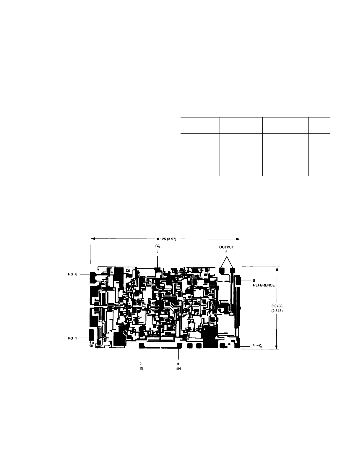
METALIZATION PHOTOGRAPH
Dimensions shown in inches and (mm).
Contact factory for latest dimensions.
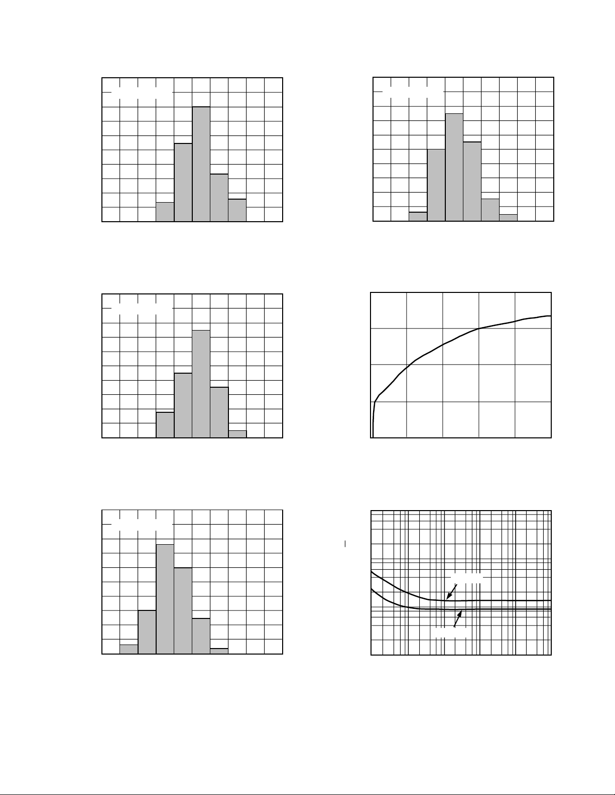
Typical Characteristics–AD621
50
0
–200
10
30
20
40
+200+1000–100
INPUT OFFSET VOLTAGE – µV
PERCENTAGE OF UNITS
SAMPLE SIZE = 90
Figure 1. Typical Distribution of V
OS,
Gain = 10
50
0
–80
10
30
20
40
+80+400–40
INPUT OFFSET VOLTAGE – µV
PERCENTAGE OF UNITS
SAMPLE SIZE = 90
Figure 2. Typical Distribution of V
OS
, Gain = 100
50
0
–400
10
30
20
40
+400+2000–200
INPUT OFFSET CURRENT – pA
PERCENTAGE OF UNITS
SAMPLE SIZE = 90
Figure 3. Typical Distribution of Input Offset Current
50
0
–800
10
30
20
40
+800+4000–400
INPUT BIAS CURRENT – pA
PERCENTAGE OF UNITS
SAMPLE SIZE = 90
Figure 4. Typical Distribution of Input Bias Current
CHANGE IN OFFSET VOLTAGE – µV
1.5
0.5
WARM-UP TIME – Minutes
2
0
051
1
432
Figure 5. Change in Input Offset Voltage vs. Warm-Up Time
1
10
100 1k
FREQUENCY – Hz
1
10
100
1000
10k
100k
VOLTAGE NOISE – nV/
√
Hz
GAIN = 10
GAIN = 100
Figure 6. Voltage Noise Spectral Density
REV. A
–5–
 Loading...