


 Loading...
1024-/256-Position, 1% Resistor Tolerance Error, SPI Interface and 50-TP Memory Digital Rheostat
FEATURES
Single-channel, 1024-/256-position resolution 20 kΩ, 50 kΩ, 100 kΩ nominal resistance Maximum ±1% nominal resistor tolerance error 50-times programmable (50-TP) wiper memory Rheostat mode temperature coefficient: 5 ppm/°C 2.7 V to 5.5 V single-supply operation
±2.5 V to ±2.75 V dual-supply operation for ac or bipolar operations
SPI-compatible interface Wiper setting readback
Power on refreshed from 50-TP memory
Thin LFCSP, 10-lead, 3 mm × 3 mm × 0.8 mm package Compact MSOP, 10-lead, 3 mm × 4.9 mm × 1.1 mm package
APPLICATIONS
Mechanical rheostat replacements
Op-amp: variable gain control
Instrumentation: gain, offset adjustment
Programmable voltage to current conversions
Programmable filters, delays, time constants
Programmable power supply
Sensor calibration
GENERAL DESCRIPTION
The AD5270/AD52711 are single-channel, 1024-/256-position digital rheostats that combine industry leading variable resistor performance with nonvolatile memory (NVM) in a compact package.
The AD5270/AD5271 ensure less than 1% end-to-end resistor tolerance error and offer 50-times programmable (50-TP) memory.
The guaranteed industry leading low resistor tolerance error feature simplifies open-loop applications as well as precision calibration and tolerance matching applications.
1 Protected by U.S.Patent Number 7688240...;
Rev. E
Information furnished by Analog Devices is believed to be accurate and reliable. However, no responsibilityisassumedbyAnalogDevicesforitsuse,norforanyinfringementsofpatentsorother rightsofthirdpartiesthatmayresultfromitsuse.Specificationssubjecttochangewithoutnotice.No license is granted by implication or otherwise under any patent or patent rights of Analog Devices. Trademarksandregisteredtrademarksarethepropertyoftheirrespectiveowners.
AD5270/AD5271
FUNCTIONAL BLOCK DIAGRAM
VDD
|
POWER-ON |
|
|
|
|
RESET |
AD5270/AD5271 |
|
|
|
|
|
||
SCLK |
|
RDAC |
|
|
|
REGISTER |
|
A |
|
|
SERIAL |
10/8 |
|
|
|
|
|
||
SYNC |
|
|
|
|
INTERFACE |
|
|
W |
|
|
|
|
|
|
DIN |
|
50-TP |
|
|
|
|
MEMORY |
|
|
SDO |
|
BLOCK |
|
|
|
|
|
|
|
|
VSS |
EXT_CAP |
GND |
08077-001 |
Figure 1.
The AD5270/AD5271 device wiper settings are controllable through the SPI digital interface. Unlimited adjustments are allowed before programming the resistance value into the 50-TP memory. The AD5270/AD5271 do not require any external voltage supply to facilitate fuse blow and there are 50 opportunities for permanent programming. During 50-TP
activation, a permanent blow fuse command freezes the resistance position (analogous to placing epoxy on a mechanical trimmer).
The AD5270/AD5271 are available in a 3 mm × 3 mm, 10-lead LFCSP package and in a 10-lead MSOP package. The parts are guaranteed to operate over the extended industrial temperature range of −40°C to +125°C.
One Technology Way, P.O. Box 9106, Norwood, MA 02062-9106, U.S.A. Tel: 781.329.4700 www.analog.com Fax: 781.461.3113 ©2009–2010 Analog Devices, Inc. All rights reserved.

AD5270/AD5271
TABLE OF CONTENTS |
|
Features .............................................................................................. |
1 |
Applications....................................................................................... |
1 |
Functional Block Diagram .............................................................. |
1 |
General Description ......................................................................... |
1 |
Revision History ............................................................................... |
2 |
Specifications..................................................................................... |
3 |
Electrical Characteristics—AD5270 .......................................... |
3 |
Electrical Characteristics—AD5271 .......................................... |
5 |
Interface Timing Specifications.................................................. |
7 |
Absolute Maximum Ratings............................................................ |
9 |
Thermal Resistance ...................................................................... |
9 |
ESD Caution.................................................................................. |
9 |
Pin Configuration and Function Descriptions........................... |
10 |
Typical Performance Characteristics ........................................... |
11 |
Test Circuits..................................................................................... |
17 |
Theory of Operation ...................................................................... |
18 |
Serial Data Interface................................................................... |
18 |
REVISION HISTORY |
|
12/10—Rev. D to Rev. E |
|
Changes to SDO Pin Description................................................. |
10 |
Changes to SDO Pin and Daisy-Chain Operation Section....... |
21 |
11/10—Rev. C to Rev. D |
|
Changes to Figure 25...................................................................... |
14 |
9/10—Rev. B to Rev. C |
|
Changes to Figure 3 Caption........................................................... |
7 |
Changes to Figure 4 Caption........................................................... |
8 |
Deleted Daisy-Chain Operation Section, Added SDO Pin and |
|
Daisy-Chain Operation Section ................................................... |
21 |
5/10—Rev. A to Rev. B |
|
Added LFCSP Throughout.............................................................. |
1 |
Changed OTP to 50-TP Throughout............................................. |
1 |
Changes to Product Title, Features, and General Description... |
1 |
Shift Register ............................................................................... |
18 |
RDAC Register............................................................................ |
18 |
50-TP Memory Block ................................................................ |
18 |
Write Protection ......................................................................... |
18 |
RDAC and 50-TP Read Operation .......................................... |
19 |
Shut-Down Mode....................................................................... |
20 |
Resistor Performance Mode...................................................... |
20 |
Reset ............................................................................................. |
20 |
SDO Pin and Daisy-Chain Operation..................................... |
21 |
RDAC Architecture.................................................................... |
21 |
Programming the Variable Resistor......................................... |
22 |
EXT_CAP Capacitor.................................................................. |
22 |
Terminal Voltage Operating Range ......................................... |
22 |
Power-Up Sequence ................................................................... |
22 |
Outline Dimensions ....................................................................... |
23 |
Ordering Guide .......................................................................... |
24 |
Changes to Table 1............................................................................. |
3 |
Added Table 3; Renumbered Sequentially ..................................... |
4 |
Changes to Table 4............................................................................. |
5 |
Added Table 6 .................................................................................... |
6 |
Changes to Table 8 and Table 9 ....................................................... |
9 |
Added Figure 6 and changes to Table 10..................................... |
10 |
Replaced Typical Performance Characteristics Section ............ |
11 |
Changes to Figure 44...................................................................... |
21 |
Updated Outline Dimensions....................................................... |
23 |
Changes to Ordering Guide .......................................................... |
24 |
3/10—Rev. 0 to Rev. A |
|
Changes to Product Title and General Description..................... |
1 |
Changes to Theory of Operation Section................................... |
14 |
10/09—Revision 0: Initial Version |
|
Rev. E | Page 2 of 24

AD5270/AD5271
SPECIFICATIONS
ELECTRICAL CHARACTERISTICS—AD5270
VDD = 2.7 V to 5.5 V, VSS = 0 V; VDD = 2.5 V to 2.75 V, VSS = −2.5 V to −2.75 V; −40°C < TA < +125°C, unless otherwise noted.
Table 1.
Parameter |
Symbol |
Test Conditions/Comments |
Min |
Typ1 |
Max |
Unit |
DC CHARACTERISTICS—RHEOSTAT MODE |
|
|
|
|
|
|
Resolution |
|
|
10 |
|
|
Bits |
Resistor Integral Nonlinearity2, 3 |
R-INL |
RAW = 20 kΩ, |VDD − VSS| = 3.0 V to 5.5 V |
−1 |
|
+1 |
LSB |
|
|
RAW = 20 kΩ, |VDD − VSS| = 2.7 V to 3.0 V |
−1 |
|
+1.5 |
LSB |
|
|
RAW = 50 kΩ, 100 kΩ |
−1 |
|
+1 |
LSB |
Resistor Differential Nonlinearity2 |
R-DNL |
|
−1 |
|
+1 |
LSB |
Nominal Resistor Tolerance |
|
|
|
|
|
|
R-Perf Mode4 |
|
See Table 2 and Table 3 |
−1 |
±0.5 |
+1 |
% |
Normal Mode |
|
|
|
±15 |
|
% |
Resistance Temperature Coefficient5, 6 |
|
Code = full scale |
|
5 |
|
ppm/°C |
Wiper Resistance |
|
Code = zero scale |
|
35 |
70 |
Ω |
|
|
|
|
|
|
|
RESISTOR TERMINALS |
|
|
|
|
|
|
Terminal Voltage Range5, 7 |
|
|
VSS |
|
VDD |
V |
Capacitance5 A |
|
f = 1 MHz, measured to GND, code = |
|
90 |
|
pF |
|
|
half scale |
|
|
|
|
Capacitance5 W |
|
f = 1 MHz, measured to GND, code = |
|
40 |
|
pF |
|
|
half scale |
|
|
|
|
Common-Mode Leakage Current5 |
|
VA = VW |
|
|
50 |
nA |
DIGITAL INPUTS |
|
|
|
|
|
|
Input Logic5 |
|
|
|
|
|
|
High |
VINH |
|
2.0 |
|
|
V |
Low |
VINL |
|
|
|
0.8 |
V |
Input Current |
IIN |
|
|
±1 |
|
μA |
Input Capacitance5 |
CIN |
|
|
5 |
|
pF |
DIGITAL OUTPUT |
|
|
|
|
|
|
Output Voltage5 |
|
|
|
|
|
|
High |
VOH |
RPULL_UP = 2.2 kΩ to VDD |
VDD − 0.1 |
|
|
V |
Low |
VOL |
RPULL_UP = 2.2 kΩ to VDD |
|
|
|
|
|
|
VDD = 2.7 V to 5.5 V, VSS = 0 V |
|
|
0.4 |
V |
|
|
VDD = 2.5 V to 2.75 V, VSS = −2.5 V to −2.75 V |
|
|
0.6 |
V |
Tristate Leakage Current |
|
|
−1 |
|
+1 |
μA |
Output Capacitance5 |
|
|
|
5 |
|
pF |
POWER SUPPLIES |
|
|
|
|
|
|
Single-Supply Power Range |
|
VSS = 0 V |
2.7 |
|
5.5 |
V |
Dual-Supply Power Range |
|
|
±2.5 |
|
±2.75 |
V |
Supply Current |
|
|
|
|
|
|
Positive |
IDD |
|
|
|
1 |
μA |
Negative |
ISS |
|
−1 |
|
|
μA |
50-TP Store Current5, 8 |
|
|
|
|
|
|
Positive |
IDD_OTP_STORE |
|
|
4 |
|
mA |
Negative |
ISS_OTP_STORE |
|
|
−4 |
|
mA |
OTP Read Current5, 9 |
|
|
|
|
|
|
Positive |
IDD_OTP_READ |
|
|
|
500 |
μA |
Negative |
ISS_OTP_READ |
|
−500 |
|
|
μA |
Rev. E | Page 3 of 24

AD5270/AD5271
Parameter |
Symbol |
Test Conditions/Comments |
Min |
Typ1 |
Max |
Unit |
Power Dissipation10 |
|
VIH = VDD or VIL = GND |
|
|
5.5 |
μW |
Power Supply Rejection Ratio5 |
PSRR |
ΔVDD/ΔVSS = ±5 V ± 10% |
|
|
|
dB |
|
|
RAW = 20 kΩ |
|
−66 |
−55 |
|
|
|
RAW = 50 kΩ |
|
−75 |
−67 |
|
|
|
RAW = 100 kΩ |
|
−78 |
−70 |
|
DYNAMIC CHARACTERISTICS5, 11 |
|
|
|
|
|
|
Bandwidth |
|
−3 dB, RAW = 10 kΩ, Terminal W, |
|
|
|
kHz |
|
|
see Figure 42 |
|
|
|
|
|
|
RAW = 20 kΩ |
|
300 |
|
|
|
|
RAW = 50 kΩ |
|
120 |
|
|
|
|
RAW = 100 kΩ |
|
60 |
|
|
Total Harmonic Distortion |
|
VA = 1 V rms, f = 1 kHz, |
|
|
|
dB |
|
|
code = half scale |
|
|
|
|
|
|
RAW = 20 kΩ |
|
−90 |
|
|
|
|
RAW = 50 kΩ |
|
−88 |
|
|
|
|
RAW= 100 kΩ |
|
−85 |
|
|
Resistor Noise Density |
|
Code = half scale, TA = 25°C |
|
|
|
nV/√Hz |
|
|
RAW = 20 kΩ |
|
50 |
|
|
|
|
RAW = 50 kΩ |
|
25 |
|
|
|
|
RAW = 100 kΩ |
|
32 |
|
|
1 Typical specifications represent average readings at 25°C, VDD = 5 V, and VSS = 0 V.
2Resistor position nonlinearity error (R-INL) is the deviation from an ideal value measured between the maximum resistance and the minimum resistance wiper positions. R-DNL measures the relative step change from ideal between successive tap positions.
3 The maximum current in each code is defined by IAW = (VDD − 1)/RAW.
4 The terms resistor performance mode and R-Perf mode are used interchangeably. See the Resistor Performance Mode section. 5 Guaranteed by design and not subject to production test.
6 See Figure 25 for more details.
7 Resistor Terminal A and Resistor Terminal W have no limitations on polarity with respect to each other. Dual-supply operation enables ground referenced bipolar signal adjustment.
8 Different from operating current, the supply current for the fuse program lasts approximately 55 ms. 9 Different from operating current, the supply current for the fuse read lasts approximately 500 ns.
10PDISS is calculated from (IDD × VDD) + (ISS × VSS).
11All dynamic characteristics use VDD = +2.5 V, VSS = −2.5 V.
Table 2. AD5270—20 kΩ Resistor Performance Mode Code Range
Resistor Tolerance Per Code |
|VDD − VSS| = 4.5 V to 5.5 V |
R-TOLERANCE |
|
1% R-Tolerance |
From 0x078 to 0x3FF |
2% R-Tolerance |
From 0x037 to 0x3FF |
3% R-Tolerance |
From 0x028 to 0x3FF |
|
|
Table 3. AD5270—50 kΩ and 100 kΩ Resistor Performance Mode Code Range
Resistor Tolerance Per Code |
RAW = 50 kΩ |
|
|
R-TOLERANCE |
|
1% R-Tolerance |
From 0x078 to 0x3FF |
2% R-Tolerance |
From 0x055 to 0x3FF |
3% R-Tolerance |
From 0x032 to 0x3FF |
|VDD − VSS| = 2.7 V to 4.5 V
From 0x0BE to 0x3FF From 0x055 to 0x3FF From 0x037 to 0x3FF
RAW = 100 kΩ
From 0x04B to 0x3FF From 0x032 to 0x3FF From 0x019 to 0x3FF
Rev. E | Page 4 of 24

AD5270/AD5271
ELECTRICAL CHARACTERISTICS—AD5271
VDD = 2.7 V to 5.5 V, VSS = 0 V; VDD = 2.5 V to 2.75 V, VSS = −2.5 V to −2.75 V; −40°C < TA < +125°C, unless otherwise noted.
Table 4.
Parameter |
Symbol |
Test Conditions/Comments |
Min |
Typ1 |
Max |
Unit |
DC CHARACTERISTICS—RHEOSTAT MODE |
|
|
|
|
|
|
Resolution |
|
|
8 |
|
|
Bits |
Resistor Integral Nonlinearity2, 3 |
R-INL |
|
−1 |
|
+1 |
LSB |
Resistor Differential Nonlinearity2 |
R-DNL |
|
−1 |
|
+1 |
LSB |
Nominal Resistor Tolerance |
|
|
|
|
|
|
R-Perf Mode4 |
|
See Table 5 and Table 6 |
−1 |
±0.5 |
+1 |
% |
Normal Mode |
|
|
|
±15 |
|
% |
Resistance Temperature Coefficient5, 6 |
|
Code = full scale |
|
5 |
|
ppm/°C |
Wiper Resistance |
|
Code = zero scale |
|
35 |
70 |
Ω |
|
|
|
|
|
|
|
RESISTOR TERMINALS |
|
|
|
|
|
|
Terminal Voltage Range5, 7 |
|
|
VSS |
|
VDD |
V |
Capacitance5 A |
|
f = 1 MHz, measured to GND, code = |
|
90 |
|
pF |
|
|
half scale |
|
|
|
|
Capacitance5 W |
|
f = 1 MHz, measured to GND, code = |
|
40 |
|
pF |
|
|
half scale |
|
|
|
|
Common-Mode Leakage Current5 |
|
VA = VW |
|
|
50 |
nA |
DIGITAL INPUTS |
|
|
|
|
|
|
Input Logic5 |
|
|
|
|
|
|
High |
VINH |
|
2.0 |
|
|
V |
Low5 |
VINL |
|
|
|
0.8 |
V |
Input Current |
IIN |
|
|
±1 |
|
μA |
Input Capacitance5 |
CIN |
|
|
5 |
|
pF |
DIGITAL OUTPUT |
|
|
|
|
|
|
Output Voltage5 |
|
|
|
|
|
|
High |
VOH |
RPULL_UP = 2.2 kΩ to VDD |
VDD − 0.1 |
|
|
V |
Low |
VOL |
RPULL_UP = 2.2 kΩ to VDD |
|
|
|
|
|
|
VDD = 2.7 V to 5.5 V, VSS = 0 V |
|
|
0.4 |
V |
|
|
VDD = 2.5 V to 2.75 V, VSS = −2.5 V to −2.75 V |
|
|
0.6 |
V |
Tristate Leakage Current |
|
|
−1 |
|
+1 |
μA |
Output Capacitance5 |
|
|
|
5 |
|
pF |
POWER SUPPLIES |
|
|
|
|
|
|
Single-Supply Power Range |
|
VSS = 0 V |
2.7 |
|
5.5 |
V |
Dual-Supply Power Range |
|
|
±2.5 |
|
±2.75 |
V |
Supply Current |
|
|
|
|
|
|
Positive |
IDD |
|
|
|
1 |
μA |
Negative |
ISS |
|
−1 |
|
|
μA |
50-TP Store Current5, 8 |
|
|
|
|
|
|
Positive |
IDD_OTP_STORE |
|
|
4 |
|
mA |
Negative |
ISS_OTP_STORE |
|
|
−4 |
|
mA |
OTP Read Current5, 9 |
|
|
|
|
|
|
Positive |
IDD_OTP_READ |
|
|
|
500 |
μA |
Negative |
ISS_OTP_READ |
|
−500 |
|
|
μA |
Power Dissipation10 |
|
VIH = VDD or VIL = GND |
|
|
5.5 |
μW |
Power Supply Rejection Ratio5 |
PSRR |
ΔVDD/ΔVSS = ±5 V ± 10% |
|
|
|
dB |
|
|
RAW = 20 kΩ |
|
−66 |
−55 |
|
|
|
RAW = 50 kΩ |
|
−75 |
−67 |
|
|
|
RAW = 100 kΩ |
|
−78 |
−70 |
|
|
|
|
|
|
|
|
Rev. E | Page 5 of 24

AD5270/AD5271
Parameter |
Symbol |
Test Conditions/Comments |
Min |
Typ1 Max |
Unit |
DYNAMIC CHARACTERISTICS5, 11 |
|
|
|
|
|
Bandwidth |
|
−3 dB, RAW = 10 kΩ, Terminal W, see Figure 42 |
|
|
kHz |
|
|
RAW = 20 kΩ |
|
300 |
|
|
|
RAW = 50 kΩ |
|
120 |
|
|
|
RAW = 100 kΩ |
|
60 |
|
Total Harmonic Distortion |
|
VA = 1 V rms, f = 1 kHz, code = half scale |
|
|
dB |
|
|
RAW = 20 kΩ |
|
−90 |
|
|
|
RAW = 50 kΩ |
|
−88 |
|
|
|
RAW = 100 kΩ |
|
−85 |
|
Resistor Noise Density |
|
Code = half scale, TA = 25°C |
|
|
nV/√Hz |
|
|
RAW = 20 kΩ |
|
50 |
|
|
|
RAW = 50 kΩ |
|
25 |
|
|
|
RAW = 100 kΩ |
|
32 |
|
1 Typical specifications represent average readings at 25°C, VDD = 5 V, and VSS = 0 V.
2Resistor position nonlinearity error (R-INL) is the deviation from an ideal value measured between the maximum resistance and the minimum resistance wiper positions. R-DNL measures the relative step change from ideal between successive tap positions.
3 The maximum current in each code is defined by IAW = (VDD − 1)/RAW.
4 The terms resistor performance mode and R-Perf mode are used interchangeably. See the Resistor Performance Mode section. 5 Guaranteed by design and not subject to production test.
6 See Figure 25 for more details.
7Resistor Terminal A and Resistor Terminal W have no limitations on polarity with respect to each other. Dual-supply operation enables ground referenced bipolar signal adjustment.
8 Different from operating current, the supply current for the fuse program lasts approximately 55 ms. 9 Different from operating current, the supply current for the fuse read lasts approximately 500 ns.
10PDISS is calculated from (IDD × VDD) + (ISS × VSS).
11All dynamic characteristics use VDD = +2.5 V, VSS = −2.5 V.
Table 5. AD5271—20 kΩ Resistor Performance Mode Code Range
Resistor Tolerance per Code |
|VDD − VSS| = 4.5 V to 5.5 V |
R-TOLERANCE |
|
1% R-Tolerance |
From 0x1E to 0xFF |
2% R-Tolerance |
From 0x0F to 0xFF |
3% R-Tolerance |
From 0x06 to 0xFF |
|
|
Table 6. AD5271—50 kΩ and 100 kΩ Resistor Performance Mode Code Range
Resistor Tolerance per Code |
RAW = 50 kΩ |
|
|
R-TOLERANCE |
|
1% R-Tolerance |
From 0x1E to 0xFF |
2% R-Tolerance |
From 0x14 to 0xFF |
3% R-Tolerance |
From 0x0A to 0xFF |
|VDD − VSS| = 2.7 V to 4.5 V
From 0x32 to 0xFF
From 0x19 to 0xFF
From 0x0E to 0xFF
RAW = 100 kΩ
From 0x14 to 0xFF
From 0x0F to 0xFF
From 0x0A to 0xFF
Rev. E | Page 6 of 24

AD5270/AD5271
INTERFACE TIMING SPECIFICATIONS
VDD = 2.5 V to 5.5 V, VSS = 0 V; VDD = 2.5 V, VSS = −2.5 V; all specifications TMIN to TMAX, unless otherwise noted.
Table 7.
Parameter |
Limit1 |
Unit |
t12 |
20 |
ns min |
t2 |
10 |
ns min |
t3 |
10 |
ns min |
t4 |
15 |
ns min |
t5 |
5 |
ns min |
t6 |
5 |
ns min |
t7 |
1 |
ns min |
t83, 4 |
500 |
ns min |
t9 |
15 |
ns min |
t105 |
450 |
ns max |
tRDAC_R-PERF |
2 |
μs max |
tRDAC_NORMAL |
600 |
ns max |
tMEMORY_READ |
6 |
μs max |
tMEMORY_PROGRAM |
350 |
ms max |
tRESET |
0.6 |
ms max |
tPOWER-UP6 |
2 |
ms max |
Test Conditions/Comments
SCLK cycle time
SCLK high time
SCLK low time
SYNC to SCLK falling edge setup time Data setup time
Data hold time
SCLK falling edge to SYNC rising edge
Minimum SYNC high time
SYNC rising edge to next SCLK fall ignored SCLK rising edge to SDO valid
RDAC register write command execute time RDAC register write command execute time Memory readback execute time
Memory program time Reset 50-TP restore time Power-on 50-TP restore time
1 All input signals are specified with tr = tf = 1 ns/V (10% to 90% of VDD) and timed from a voltage level of (VIL + VIH)/2. 2 Maximum SCLK frequency is 50 MHz.
3 Refer to tRDAC_R-PER and tRDAC_NORMAL for RDAC register write operations.
4 Refer to tMEMORY_READ and tMEMORY_PROGRAM for memory commands operations. 5 RPULL_UP = 2.2 kΩ to VDD with a capacitance load of 168 pF.
6 Maximum time after VDD − VSS is equal to 2.5 V.
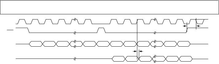
Shift Register and Timing Diagrams
|
|
|
|
|
|
|
|
DB9 (MSB) |
|
|
|
|
|
|
|
DB0 (LSB) |
|
|
|
0 |
0 |
C3 |
C2 |
C1 |
C0 |
D9 |
D8 |
D7 |
D6 |
D5 |
D4 |
D3 |
D2 |
D1 |
D0 |
|
|
|
|
|
|
|
|
|
|
|
|
DATA BITS |
|
|
|
-002 |
|
|
|
|
|
|
CONTROL BITS |
|
|
|
|
|
|
|
|
|
|
08077 |
|
|
|
|
|
|
|
|
|
Figure 2. Shift Register Content |
|
|
|
|
|
||||
|
t4 |
t2 |
|
|
t1 |
|
|
|
|
|
|
|
|
|
|
t7 |
|
|
|
|
|
|
|
|
|
|
|
|
|
|
|
|
|||
|
|
|
|
|
|
|
|
|
|
|
|
|
|
|
|
||
SCLK |
|
|
|
|
|
|
|
|
|
|
|
|
|
|
|
|
t9 |
|
t8 |
|
t3 |
|
|
|
|
|
|
|
|
|
|
|
|
|
|
|
|
|
|
|
|
|
|
|
|
|
|
|
|
|
|
||
SYNC |
|
|
|
|
|
|
|
|
|
|
|
|
|
|
|
|
|
|
|
|
|
|
|
|
|
|
|
|
|
|
|
t5 |
t6 |
|
|
|
|
|
|
|
|
|
|
|
|
|
|
|
|
|
|
|
|
DIN |
0 |
0 |
|
C3 |
C2 |
|
|
D7 |
D6 |
D5 |
|
|
D2 |
D1 |
|
D0 |
|
SDO
Figure 3. Write Timing Diagram (CPOL = 0, CPHA = 1)
08077-003
Rev. E | Page 7 of 24
AD5270/AD5271
SCLK
t9
SYNC
DIN |
0 |
0 |
C3 |
D0 |
D0 |
0 |
0 |
C3 |
D1 |
D0 |
|
|
|
|
|
|
|
|
t10 |
|
|
SDO |
|
|
|
|
|
X |
X |
C3 |
D1 |
D0 |
Figure 4. Read Timing Diagram (CPOL = 0, CPHA = 1)
08077-004
Rev. E | Page 8 of 24
Loading...