


AD632TH-883B
Analog Devices AD632TH-883B, AD632TH, AD632TD-883B, AD632TD, AD632SH-883B Datasheet
...
REV. A
Information furnished by Analog Devices is believed to be accurate and
reliable. However, no responsibility is assumed by Analog Devices for its
use, nor for any infringements of patents or other rights of third parties
which may result from its use. No license is granted by implication or
otherwise under any patent or patent rights of Analog Devices.
a
AD632
One Technology Way, P.O. Box 9106, Norwood, MA 02062-9106, U.S.A.
Tel: 617/329-4700 World Wide Web Site: http://www.analog.com
Fax: 617/326-8703 © Analog Devices, Inc., 1997
Internally Trimmed
Precision IC Multiplier
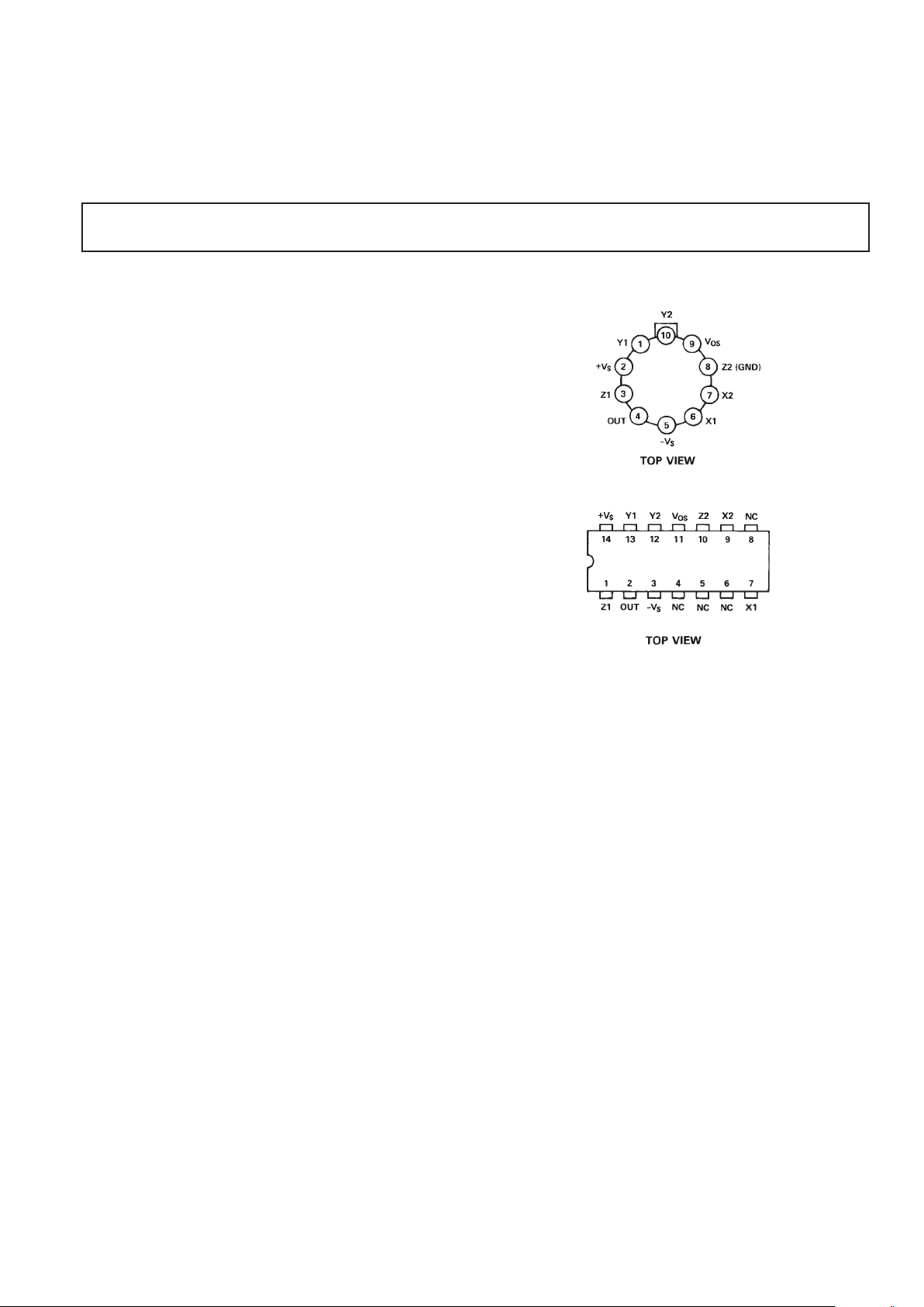
PIN CONFIGURATIONS
H-Package TO-100
D-Package TO-116
PRODUCT DESCRIPTION
The AD632 is an internally-trimmed monolithic four-quadrant
multiplier/divider. The AD632B has a maximum multiplying
error of ±0.5% without external trims.
Excellent supply rejection, low temperature coefficients and
long term stability of the on-chip thin film resistors and buried
zener reference preserve accuracy even under adverse conditions. The simplicity and flexibility of use provide an attractive
alternative approach to the solution of complex control functions.
The AD632 is pin-for-pin compatible with the industry standard
AD532 with improved specifications and a fully differential high
impedance Z-input. The AD632 is capable of providing gains of
up to X10, frequently eliminating the need for separate instrumentation amplifiers to precondition the inputs. The AD632
can be effectively employed as a variable gain differential input
amplifier with high common-mode rejection. The effectiveness
of the variable gain capability is enhanced by the inherent low
noise of the AD632: 90 µV rms.
FEATURES
Pretrimmed to ±0.5% Max 4-Quadrant Error
All Inputs (X, Y and Z) Differential, High Impedance for
[(X
1–X2
)(Y1–Y2)/10] + Z2 Transfer Function
Scale-Factor Adjustable to Provide up to X10 Gain
Low Noise Design: 90 mV rms, 10 Hz–10 kHz
Low Cost, Monolithic Construction
Excellent Long-Term Stability
APPLICATIONS
High Quality Analog Signal Processing
Differential Ratio and Percentage Computations
Algebraic and Trigonometric Function Synthesis
Accurate Voltage Controlled Oscillators and Filters
PRODUCT HIGHLIGHTS
Guaranteed Performance Over Temperature
The AD632A and AD632B are specified for maximum multi-
plying errors of ±1.0% and ±0.5% of full scale, respectively at
+25°C and are rated for operation from –25°C to +85°C.
Maximum multiplying errors of ± 2.0% (AD632S) and ±1.0%
(AD632T) are guaranteed over the extended temperature range
of –55°C to +125°C.
High Reliability
The AD632S and AD632T series are also available with
MIL-STD-883 Level B screening and all devices are available in
either the hermetically-sealed TO-100 metal can or TO-116
ceramic DIP package.

–2–
REV. A
AD632–SPECIFICATIONS
(@ +258C, V
S
= ±15 V, R ≥ 2 kV unless otherwise noted)
AD632A AD632B AD632S AD632T
Model Min Typ Max Min Typ Max Min Typ Max Min Typ Max Units
MULTIPLIER PERFORMANCE
Transfer Function
( X
1
− X
2
)(Y
1
− Y
2
)
10V
+ Z
2
( X
1
− X
2
)(Y
1
− Y
2
)
10V
+ Z
2
( X
1
− X
2
)(Y
1
− Y
2
)
10V
+ Z
2
( X
1
− X
2
)(Y
1
− Y
2
)
10V
+ Z
2
Total Error
1
(–10 V ≤ X, Y ≤ +10 V) 61.0 60.5 61.0 60.5 %
T
A
= Min to Max 61.5 61.0 62.0 61.0 %
Total Error vs. Temperature ±0.022 ±0.015 60.02 60.01 %/°C
Scale Factor Error
(SF = 10.000 V Nominal)
2
±0.25 ±0.1 ±0.25 ±0.1 %
Temperature-Coefficient of
Scaling-Voltage ±0.02 60.01 ±0.2 60.005 %/°C
Supply Rejection (±15 V ± 1 V) ±0.01 ±0.01 ±0.01 ±0.01 %
Nonlinearity, X (X = 20 V p-p, Y = 10 V) ±0.4 ±0.2 ±0.3 ±0.4 ±0.2 ±0.3 %
Nonlinearity, Y (Y = 20 V p-p, X = 10 V) ±0.2 ±0.1 ±0.1 ±0.2 ±0.1 ±0.1 %
Feedthrough
3
, X (Y Nulled,
X = 20 V p-p 50 Hz) ±0.3 ±0.15 ±0.3 ±0.3 ±0.15 ±0.3 %
Feedthrough
3
, Y (X Nulled,
Y = 20 V p-p 50 Hz) ±0.01 ±0.01 ±0.1 ±0.01 ±0.01 ±0.1 %
Output Offset Voltage ±5 630 ±2 ±15 ±5 630 ±2 ±15 mV
Output Offset Voltage Drift 200 100 500 300 µV/°C
DYNAMICS
Small Signal BW, (V
OUT
= 0.1 rms) 1111MHz
1% Amplitude Error (C
LOAD
= 1000 pF) 50 50 50 50 kHz
Slew Rate (V
OUT
20 p-p) 20 20 20 20 V/µs
Settling Time (to 1%, ∆V
OUT
= 20 V)2222µs
NOISE
Noise Spectral-Density SF = 10 V 0.8 0.8 0.8 0.8 µV/√Hz
SF = 3 V
4
0.4 0.4 0.4 0.4 µV/√Hz
Wideband Noise A = 10 Hz to 5 MHz 1.0 1 .0 1.0 1.0 mV rms
P = 10 Hz to 10 kHz 90 90 90 90 µV/rms
OUTPUT
Output Voltage Swing 611 611 611 611 V
Output Impedance (f ≤ 1 kHz) 0.1 0.1 0.1 0.1 Ω
Output Short Circuit Current
(R
L
= 0, TA = Min to Max) 30 30 30 30 mA
Amplifier Open Loop Gain (f = 50 Hz) 70 70 70 70 dB
INPUT AMPLIFIERS (X, Y and Z)
5
Signal Voltage Range (Diff. or CM ±10 ±10 ±10 ±10 V
Operating Diff.) ±12 ±12 ±12 ±12 V
Offset Voltage X, Y ±5 620 ±2 610 ±5 620 ±2 610 mV
Offset Voltage Drift X, Y 100 50 100 150 µV/°C
Offset Voltage Z ±5 630 ±2 615 ±5 630 ±2 615 mV
Offset Voltage Drift Z 200 100 500 300 µV/°C
CMRR 60 80 70 90 60 80 70 90 dB
Bias Current 0.8 2.0 0.8 2.0 0.8 2.0 0.8 2.0 µA
Offset Current 0.1 0. I 0.1 0.1 µA
Differential Resistance 10 10 1 0 10 MΩ
DIVIDER PERFORMANCE
Transfer Function (X1 > X2)
10V
( Z
2
− Z
1
)
( X
1
− X
2
)
+Y
1
10V
( Z
2
− Z
1
)
( X
1
− X
2
)
+Y
1
10V
( Z
2
− Z
1
)
( X
1
− X
2
)
+Y
1
10V
( Z
2
− Z
1
)
( X
1
− X
2
)
+Y
1
Total Error
1
(X = 10 V, –10 V ≤ Z ≤ +10 V) ±0.75 ±0.35 ±0.75 ±0.35 %
(X = 1 V, –1 V ≤ Z ≤ +1 V) ±2.0 ±1.0 ±2.0 ±1.0 %
(0.1 V ≤ X ≤ 10 V, –10 V ≤ Z ≤ 10 V) ±2.5 ±1.0 ±2.5 ±1.0 %
SQUARER PERFORMANCE
Transfer Function
( X
1
− X
2
)
2
10V
+ Z
2
( X
1
− X
2
)
2
10V
+ Z
2
( X
1
− X
2
)
2
10V
+ Z
2
( X
1
− X
2
)
2
10V
+ Z
2
Total Error (–10 V ≤ X ≤ 10 V) ±0.6 ±0.3 ±0.6 ±0.3 %
S
QUARE-ROOTER PERFORMANCE
Transfer Function, (Z
1
≤ Z
2
)
10V (Z
2
− Z1) + X
2
10V (Z
2
− Z1) + X
2
10V (Z
2
− Z1) + X
2
10V (Z
2
− Z1) + X
2
Total Error
1
(1 V ≤ Z ≤ 10 V) ±1.0 ±0.5 ±1.0 ±0.5 %
 Loading...