


 Loading...
Serial Input, Voltage Output
12-/14-Bit Digital-to-Analog Converters
FEATURES
Pin-compatible 12-, 14-bit digital-to-analog converters Serial input, voltage output
Maximum output voltage range of ±10 V Data readback
3-wire serial interface
Clear function to a user-defined voltage Power-down function
Serial data output for daisy-chaining 16-lead TSSOP
APPLICATIONS
Industrial automation
Automatic test equipment
Process control
General-purpose instrumentation
GENERAL DESCRIPTION
The AD5530/AD5531 are single 12and 14-bit (respectively) serial input, voltage output digital-to-analog converters (DAC).
They utilize a versatile 3-wire interface that is compatible with SPI®, QSPI™, MICROWIRE™, and DSP interface standards. Data is presented to the part in a 16-bit serial word format. Serial data is available on the SDO pin for daisy-chaining purposes. Data readback allows the user to read the contents of the DAC register via the SDO pin.
Rev. B
Information furnished by Analog Devices is believed to be accurate and reliable. However, no responsibilityisassumedbyAnalogDevicesforitsuse,norforanyinfringementsofpatentsorother rightsofthirdpartiesthatmayresultfromitsuse.Specificationssubjecttochangewithoutnotice.No license is granted by implication or otherwise under any patent or patent rights of Analog Devices. Trademarksandregisteredtrademarksarethepropertyoftheirrespectiveowners.
AD5530/AD5531
FUNCTIONAL BLOCK DIAGRAM
|
VSS |
VDD |
|
|
|
REFIN |
|
|
AD5530/AD5531 |
|
|
|
R |
R |
12-/14-BIT |
|
|
|
DAC |
VOUT |
|||
|
|
||||
|
|
|
R |
||
REFAGND |
|
|
|
||
|
|
|
|
||
LDAC |
|
|
R |
|
|
DAC REGISTER |
|
DUTGND |
|||
RBEN |
|
||||
|
|
|
CLR |
||
|
|
|
|
||
SDIN |
SHIFT REGISTER |
POWER-DOWN |
PD |
||
CONTROL LOGIC |
|||||
|
|||||
GND |
SCLK |
SYNC |
SDO |
00938-001 |
|
Figure 1.
The DAC output is buffered by a gain of two amplifier and referenced to the potential at DUTGND. LDAC can be used to update the output of the DAC asynchronously. A power-down pin (PD) allows the DAC to be put into a low power state, and a CLR pin allows the output to be cleared to a user-defined voltage, the potential at DUTGND.
The AD5530/AD5531 are available in 16-lead TSSOP.
One Technology Way, P.O. Box 9106, Norwood, MA 02062-9106, U.S.A.
Tel: 781.329.4700 |
www.analog.com |
Fax: 781.461.3113 |
©2007 Analog Devices, Inc. All rights reserved. |

AD5530/AD5531
TABLE OF CONTENTS |
|
|
Features .............................................................................................. |
|
1 |
Applications....................................................................................... |
|
1 |
Functional Block Diagram .............................................................. |
|
1 |
General Description ......................................................................... |
|
1 |
Revision History ............................................................................... |
|
2 |
Specifications..................................................................................... |
|
3 |
AC Performance Characteristics ................................................ |
|
5 |
Standalone Timing Characteristics............................................ |
|
5 |
Daisy-Chaining and Readback Timing Characteristics |
.......... 6 |
|
Absolute Maximum Ratings............................................................ |
|
7 |
ESD Caution.................................................................................. |
|
7 |
Pin Configuration and Function Descriptions............................. |
|
8 |
Typical Performance Characteristics ............................................. |
|
9 |
Terminology .................................................................................... |
|
12 |
Theory of Operation ...................................................................... |
|
13 |
DAC Architecture....................................................................... |
|
13 |
Serial Interface ............................................................................ |
|
13 |
REVISION HISTORY |
|
|
1/07—Rev. A to Rev. B |
|
|
Updated Format.................................................................. |
Universal |
|
Changes to Figure 28...................................................................... |
|
17 |
3/06—Rev. 0 to Rev. A |
|
|
Change to Table 3 ............................................................................. |
|
5 |
Change to Figure 4 ........................................................................... |
|
8 |
Change to Output Voltage Section............................................... |
|
14 |
Change to Ordering Guide............................................................ |
|
18 |
5/02—Revision 0: Initial Version |
|
|
PD Function................................................................................ |
13 |
Readback Function .................................................................... |
13 |
CLR Function.............................................................................. |
13 |
Output Voltage............................................................................ |
14 |
Bipolar Configuration................................................................ |
14 |
Microprocessor Interfacing........................................................... |
15 |
AD5530/AD5531 to ADSP-21xx.............................................. |
15 |
AD5530/AD5531 to 8051 Interface ......................................... |
15 |
AD5530/AD5531 to MC68HC11 Interface ............................ |
15 |
Applications Information .............................................................. |
17 |
Optocoupler Interface................................................................ |
17 |
Serial Interface to Multiple AD5530s or AD5531s ................ |
17 |
Daisy-Chaining Interface with Multiple AD5530s or |
|
AD5531s ...................................................................................... |
17 |
Outline Dimensions ....................................................................... |
18 |
Ordering Guide .......................................................................... |
18 |
Rev. B | Page 2 of 20

AD5530/AD5531
SPECIFICATIONS
VDD = 15 V ± 10%; VSS = −15 V ± 10%; GND = 0 V; RL = 5 kΩ and CL = 220 pF to GND. All specifications TMIN to TMAX, unless otherwise noted.
Table 1.
Parameter1 |
AD5530 |
AD5531 |
Unit |
ACCURACY |
|
|
|
Resolution |
12 |
14 |
Bits |
Relative Accuracy |
±1 |
±2 |
LSB max |
Differential Nonlinearity |
±1 |
±1 |
LSB max |
Zero-Scale Error |
±2 |
±8 |
LSB max |
Full-Scale Error |
±2 |
±8 |
LSB max |
Gain Error |
±1 |
±4 |
LSB typ |
Gain Temperature Coefficient2 |
0.5 |
0.5 |
ppm FSR/°C typ |
|
10 |
10 |
ppm FSR/°C max |
|
|
|
|
REFERENCE INPUTS2 |
|
|
|
Reference Input Range |
0 to 5 |
0 to 5 |
V min to V max |
DC Input Resistance |
100 |
100 |
MΩ typ |
Input Current |
±1 |
±1 |
μA max |
DUTGND INPUT2 |
|
|
|
DC Input Impedance |
60 |
60 |
kΩ typ |
Max Input Current |
±0.3 |
±0.3 |
mA typ |
Input Range |
−4 to +4 |
−4 to +4 |
V min to V max |
|
|
|
|
O/P CHARACTERISTICS2 |
|
|
|
Output Voltage Swing |
±10 |
±10 |
V max |
Short-Circuit Current |
15 |
15 |
mA max |
Resistive Load |
5 |
5 |
kΩ min |
Capacitive Load |
1200 |
1200 |
pF max |
DC Output Impedance |
0.5 |
0.5 |
Ω max |
DIGITAL I/O |
|
|
|
VINH, Input High Voltage |
2.4 |
2.4 |
V min |
VINL, Input Low Voltage |
0.8 |
0.8 |
V max |
IINH, Input Current |
±10 |
±10 |
μA max |
CIN, Input Capacitance2 |
10 |
10 |
pF max |
SDO VOL, Output Low Voltage |
0.4 |
0.4 |
V max |
POWER REQUIREMENTS |
|
|
|
VDD/VSS |
+15/−15 |
+15/−15 |
V nom |
Power Supply Sensitivity |
|
|
|
ΔFull Scale/ΔVDD |
110 |
110 |
dB typ |
ΔFull Scale/ΔVSS |
100 |
100 |
dB typ |
IDD |
2 |
2 |
mA max |
ISS |
2 |
2 |
mA max |
IDD in Power-Down |
150 |
150 |
μA max |
|
|
|
|
Test Conditions/Comments
Guaranteed monotonic over temperature Typically within ±1 LSB
Typically within ±1 LSB
Max output range ±10 V
Per input, typically ±20 nA
Max output range ±10 V
To 0 V
To 0 V
Total for all pins 3 pF typical ISINK = 1 mA
±10% for specified performance
Outputs unloaded
Outputs unloaded
Typically 50 μA
1 Temperature range for B Version: −40°C to +85°C.
2 Guaranteed by design, not subject to production test.
Rev. B | Page 3 of 20

AD5530/AD5531
VDD = 12 V ± 10%; VSS = −12 V ± 10%; GND = 0 V; RL = 5 kΩ and CL = 220 pF to GND; TA = TMIN to TMAX, unless otherwise noted.
Table 2.
Parameter1 |
AD5530 |
AD5531 |
Unit |
Test Conditions/Comments |
ACCURACY |
|
|
|
|
Resolution |
12 |
14 |
Bits |
|
Relative Accuracy |
±1 |
±2 |
LSB max |
|
Differential Nonlinearity |
±1 |
±1 |
LSB max |
Guaranteed monotonic over temperature |
Zero-Scale Error |
±2 |
±8 |
LSB max |
Typically within ±1 LSB |
Full-Scale Error |
±2 |
±8 |
LSB max |
Typically within ±1 LSB |
Gain Error |
±1 |
±4 |
LSB typ |
|
Gain Temperature Coefficient2 |
0.5 |
0.5 |
ppm FSR/°C typ |
|
|
10 |
10 |
ppm FSR/°C max |
|
REFERENCE INPUTS2 |
|
|
|
|
Reference Input Range |
0 to 4.096 |
0 to 4.096 |
V min to V max |
Max output range ±8.192 V |
DC Input Resistance |
100 |
100 |
MΩ typ |
|
Input Current |
±1 |
±1 |
μA max |
Per input, typically ±20 nA |
|
|
|
|
|
DUTGND INPUT2 |
|
|
|
|
DC Input Impedance |
60 |
60 |
kΩ typ |
|
Max Input Current |
±0.3 |
±0.3 |
mA typ |
|
Input Range |
−3 to +3 |
−3 to +3 |
V min to V max |
Max output range ±8.192 V |
O/P CHARACTERISTICS2 |
|
|
|
|
Output Voltage Swing |
±8.192 |
±8.192 |
V max |
|
Short-Circuit Current |
15 |
15 |
mA max |
|
Resistive Load |
5 |
5 |
kΩ min |
To 0 V |
Capacitive Load |
1200 |
1200 |
pF max |
To 0 V |
DC Output Impedance |
0.5 |
0.5 |
Ω max |
|
|
|
|
|
|
DIGITAL I/O |
|
|
|
|
VINH, Input High Voltage |
2.4 |
2.4 |
V min |
|
VINL, Input Low Voltage |
0.8 |
0.8 |
V max |
|
IINH, Input Current |
±10 |
±10 |
μA max |
Total for all pins |
CIN, Input Capacitance2 |
10 |
10 |
pF max |
3 pF typical |
SDO VOL, Output Low Voltage |
0.4 |
0.4 |
V max |
ISINK = 1 mA |
|
|
|
|
|
POWER REQUIREMENTS |
|
|
|
|
VDD/VSS |
+12/−12 |
+12/−12 |
V nom |
±10% for specified performance |
Power Supply Sensitivity |
|
|
|
|
ΔFull Scale/ΔVDD |
110 |
110 |
dB typ |
|
ΔFull Scale/ΔVSS |
100 |
100 |
dB typ |
|
IDD |
2 |
2 |
mA max |
Outputs unloaded |
ISS |
2 |
2 |
mA max |
Outputs unloaded |
IDD in Power-Down |
150 |
150 |
μA max |
Typically 50 μA |
1 Temperature range for B Version: −40°C to +85°C.
2 Guaranteed by design, not subject to production test.
Rev. B | Page 4 of 20
AD5530/AD5531
AC PERFORMANCE CHARACTERISTICS
VDD = 10.8 V to 16.5 V, VSS = −10.8 V to −16.5 V; GND = 0 V; RL = 5 kΩ and CL = 220 pF to GND. All specifications TMIN to TMAX, unless otherwise noted.
Table 3.
Parameter |
B Version |
Unit |
Test Conditions/Comments |
|
|
|
|
DYNAMIC PERFORMANCE |
|
|
|
Output Voltage Settling Time |
20 |
μs typ |
Full-scale change to ±½ LSB. DAC latch contents alternately |
|
|
|
loaded with all 0s and all 1s. |
Slew Rate |
1.3 |
V/μs typ |
|
Digital-to-Analog Glitch Impulse |
120 |
nV-s typ |
DAC latch alternately loaded with 0x0FFF and 0x1000. Not |
|
|
|
dependent on load conditions. |
Digital Feedthrough |
0.5 |
nV-s typ |
Effect of input bus activity on DAC output under test. |
Output Noise Spectral Density @ 1 kHz |
100 |
nV/√Hz typ |
All 1s loaded to DAC. |
|
|
|
|
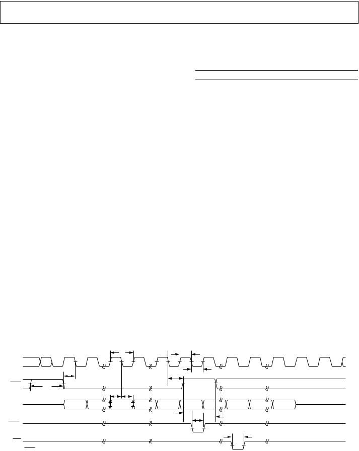
STANDALONE TIMING CHARACTERISTICS
VDD = 10.8 V to 16.5 V, VSS = −10.8 V to −16.5 V; GND = 0 V; RL = 5 kΩ and CL = 220 pF to GND. All specifications TMIN to TMAX, unless otherwise noted.
Table 4.
Parameter1, 2 |
Limit at TMIN, TMAX |
Unit |
|
Description |
|||||||||||
fMAX |
7 |
MHz max |
|
SCLK frequency |
|||||||||||
t1 |
140 |
ns min |
|
SCLK cycle time |
|||||||||||
t2 |
60 |
ns min |
|
SCLK low time |
|||||||||||
t3 |
60 |
ns min |
|
SCLK high time |
|||||||||||
t4 |
50 |
ns min |
|
|
|
|
|
to SCLK falling edge setup time |
|||||||
|
SYNC |
|
|
||||||||||||
t5 |
40 |
ns min |
|
|
|
|
|
|
|
|
|
|
|||
|
SCLK falling edge to |
SYNC |
rising edge |
||||||||||||
t6 |
50 |
ns min |
|
|
|
|
|
|
|
|
|||||
|
Min |
SYNC |
high time |
||||||||||||
t7 |
40 |
ns min |
|
Data setup time |
|||||||||||
t8 |
15 |
ns min |
|
Data hold time |
|||||||||||
t9 |
5 |
ns min |
|
|
|
|
high to |
|
|
low |
|||||
|
SYNC |
|
|
LDAC |
|||||||||||
t10 |
50 |
ns min |
|
|
|
pulse width |
|||||||||
|
LDAC |
|
|||||||||||||
t11 |
5 |
ns min |
|
|
|
|
|||||||||
|
LDAC |
high to |
SYNC |
low |
|||||||||||
t12 |
50 |
ns min |
|
|
|||||||||||
|
CLR |
pulse width |
|||||||||||||
1 Guaranteed by design, not subject to production test.
2Sample tested during initial release and after any redesign or process change that can affect this parameter. All input signals are measured with tR = tF = 5 ns (10% to 90% of VDD) and timed from a voltage level of (VIL + VIH)/2.
|
|
|
t1 |
t3 |
SCLK |
|
|
|
|
|
t4 |
|
|
t2 |
|
|
|
t5 |
|
|
|
|
|
|
SYNC |
t6 |
|
t7 t8 |
|
|
MSB |
|
LSB |
|
|
|
|
||
SDIN |
DB15 |
DB14 |
DB11 |
DB0 |
t9 
 t11
t11
LDAC1 |
t10 |
t12
CLR
1LDAC CAN BE TIED PERMANENTLY LOW, IF REQUIRED.
Figure 2. Timing Diagram for Standalone Mode
00938-002
Rev. B | Page 5 of 20

AD5530/AD5531
DAISY-CHAINING AND READBACK TIMING CHARACTERISTICS
VDD = 10.8 V to 16.5 V, VSS = −10.8 V to −16.5 V; GND = 0 V; RL = 5 kΩ and CL = 220 pF to GND. All specifications TMIN to TMAX, unless otherwise noted.
Table 5.
Parameter1, 2, 3 |
Limit at TMIN, TMAX |
Unit |
|
Description |
||||||||
fMAX |
2 |
MHz max |
|
SCLK frequency |
||||||||
t1 |
500 |
ns min |
|
SCLK cycle time |
||||||||
t2 |
200 |
ns min |
|
SCLK low time |
||||||||
t3 |
200 |
ns min |
|
SCLK high time |
||||||||
t4 |
50 |
ns min |
|
|
|
|
|
|
|
|
|
|
|
SYNC |
to SCLK falling edge setup time |
||||||||||
t5 |
40 |
ns min |
|
|
|
|
|
|
|
|||
|
SCLK falling edge to |
SYNC |
rising edge |
|||||||||
t6 |
50 |
ns min |
|
|
|
|
|
|||||
|
Min |
SYNC |
high time |
|||||||||
t7 |
40 |
ns min |
|
Data setup time |
||||||||
t8 |
15 |
ns min |
|
Data hold time |
||||||||
t12 |
50 |
ns min |
|
|
|
|
||||||
|
CLR |
pulse width |
||||||||||
t13 |
130 |
ns min |
|
SCLK falling edge to SDO valid |
||||||||
t14 |
50 |
ns max |
|
SCLK falling edge to SDO invalid |
||||||||
t15 |
50 |
ns min |
|
|
to SCLK falling edge setup time |
|||||||
|
RBEN |
|
||||||||||
t16 |
50 |
ns min |
|
|
||||||||
|
RBEN |
hold time |
||||||||||
t17 |
100 |
ns min |
|
|
||||||||
|
RBEN |
falling edge to SDO valid |
||||||||||
|
|
|
|
|
|
|
|
|
|
|
|
|
1 Guaranteed by design, not subject to production test.
2Sample tested during initial release and after any redesign or process change that can affect this parameter. All input signals are measured with tR = tF = 5 ns (10% to 90% of VDD) and timed from a voltage level of (VIL + VIH)/2.
3 SDO; RPULLUP = 5 kΩ, CL = 15 pF
|
|
|
t1 |
|
t3 |
|
|
|
SCLK |
|
|
|
|
|
|
|
|
|
t4 |
|
|
t5 |
t2 |
|
|
|
|
|
|
|
|
|
|
||
SYNC |
t6 |
|
t7 t8 |
|
|
|
|
|
|
MSB |
|
LSB |
|
|
|
|
|
|
|
|
|
|
|
|
||
SDIN |
DB15 |
DB14 |
DB11 |
DB0 |
|
|
|
|
SDO |
|
|
|
t13 |
MSB |
t14 |
|
LSB |
|
|
|
|
|
|
|||
|
|
|
|
DB15 |
DB11 |
|
DB0 |
|
(DAISY- |
|
|
|
|
|
|||
CHAINING) |
|
|
|
|
|
|
|
|
|
|
|
|
|
|
t15 |
|
t16 |
RBEN |
|
|
|
|
|
|
|
|
|
|
|
|
|
|
t17 |
t13 |
t14 |
SDO |
|
|
|
|
|
|
|
|
|
|
|
|
|
0 |
0 |
RB13 |
|
(READBACK) |
|
|
|
|
|
|||
|
|
|
|
|
MSB |
|
|
|
|
|
|
|
|
|
|
|
Figure 3. Timing Diagram for Daisy-Chaining and Readback Mode
RB0
LSB
00938-003
Rev. B | Page 6 of 20
Loading...