


 Loading...
2.5 V to 5.5 V, 230 μA, Dual Rail-to-Rail, Voltage Output 8-/10-/12-Bit DACs
FEATURES
AD5302: Two 8-bit buffered DACs in 1 package A version: ±1 LSB INL, B version: ±0.5 LSB INL AD5312: Two 10-bit buffered DACs in 1 package
A version: ±4 LSB INL, B version: ±2 LSB INL AD5322: Two 12-bit buffered DACs in 1 package A version: ±16 LSB INL, B version: ±8 LSB INL
10-lead MSOP
Micropower operation: 300 μA @ 5 V (including reference current)
Power-down to 200 nA @ 5 V, 50 nA @ 3 V 2.5 V to 5.5 V power supply Double-buffered input logic
Guaranteed monotonic by design over all codes Buffered/Unbuffered reference input options
0 V to VREF output voltage Power-on-reset to 0 V
Simultaneous update of DAC outputs via LDAC
Low power serial interface with Schmitt-triggered inputs On-chip rail-to-rail output buffer amplifiers
Qualified for automotive applications
APPLICATIONS
Portable battery-powered instruments Digital gain and offset adjustment Programmable voltage and current sources Programmable attenuators
AD5302/AD5312/AD5322
GENERAL DESCRIPTION
The AD5302/AD5312/AD5322 are dual 8-, 10-, and 12-bit buffered voltage output DACs in a 10-lead MSOP that operate from a single 2.5 V to 5.5 V supply, consuming 230 μA at 3 V. Their on-chip output amplifiers allow the outputs to swing rail- to-rail with a slew rate of 0.7 V/μs. The AD5302/AD5312/AD5322 utilize a versatile 3-wire serial interface that operates at clock rates up to 30 MHz and is compatible with standard SPI®, QSPI™, MICROWIRE™, and DSP interface standards.
The references for the two DACs are derived from two reference pins (one per DAC). The reference inputs can be configured as buffered or unbuffered inputs. The outputs of both DACs can be
updated simultaneously using the asynchronous LDAC input. The parts incorporate a power-on reset circuit, which ensures that the DAC outputs power-up to 0 V and remain there until a valid write takes place to the device. The parts contain a powerdown feature that reduces the current consumption of the devices to 200 nA at 5 V (50 nA at 3 V) and provides softwareselectable output loads while in power-down mode.
The low power consumption of these parts in normal operation makes them ideally suited for portable battery-operated equipment. The power consumption is 1.5 mW at 5 V, 0.7 mW at 3 V, reducing to 1 μW in power-down mode.
FUNCTIONAL BLOCK DIAGRAM
|
|
VDD |
VREFA |
|
|
|
POWER-ON |
|
|
AD5302/AD5312/AD5322 |
|
|
RESET |
|
|
|
|
|
INPUT |
DAC |
STRING |
BUFFER |
VOUTA |
|
REGISTER |
REGISTER |
DAC |
||
SYNC |
INTERFACE |
|
|
|
|
|
|
POWER-DOWN |
RESISTOR |
||
SCLK |
LOGIC |
|
|||
|
|
LOGIC |
|
NETWORK |
|
DIN |
INPUT |
DAC |
STRING |
|
|
|
BUFFER |
VOUTB |
|||
|
REGISTER |
REGISTER |
DAC |
||
|
|
|
|||
|
|
|
|
|
RESISTOR |
|
|
|
|
|
NETWORK |
|
LDAC |
|
VREFB |
|
00928-001 |
|
|
|
GND |
||
Figure 1.
Rev. D
Information furnished by Analog Devices is believed to be accurate and reliable. However, no responsibilityisassumedbyAnalogDevicesforitsuse,norforanyinfringementsofpatentsorother rightsofthirdpartiesthatmayresultfromitsuse.Specificationssubjecttochangewithoutnotice.No license is granted by implication or otherwise under any patent or patent rights of Analog Devices. Trademarksandregisteredtrademarksarethepropertyoftheirrespectiveowners.
One Technology Way, P.O. Box 9106, Norwood, MA 02062-9106, U.S.A. Tel: 781.329.4700 www.analog.com Fax: 781.461.3113 © 2006-2011 Analog Devices, Inc. All rights reserved.

AD5302/AD5312/AD5322
TABLE OF CONTENTS |
|
Features .............................................................................................. |
1 |
Applications....................................................................................... |
1 |
General Description ......................................................................... |
1 |
Functional Block Diagram .............................................................. |
1 |
Revision History ............................................................................... |
2 |
Specifications..................................................................................... |
3 |
AC Specifications.......................................................................... |
4 |
Timing Characteristics ................................................................ |
5 |
Absolute Maximum Ratings............................................................ |
7 |
ESD Caution.................................................................................. |
7 |
Pin Configuration and Function Descriptions............................. |
8 |
Terminology ...................................................................................... |
9 |
Typical Performance Characteristics ........................................... |
10 |
Functional Description .................................................................. |
14 |
Digital-to-Analog Section ......................................................... |
14 |
Resistor String............................................................................. |
14 |
DAC Reference Inputs ............................................................... |
14 |
Output Amplifier........................................................................ |
14 |
Power-On Reset .......................................................................... |
14 |
Serial Interface ................................................................................ |
15 |
Input Shift Register..................................................................... |
15 |
REVISION HISTORY |
|
5/11—Rev. C to Rev. D |
|
Added Automotive Products Information ................. |
Throughout |
Updated Outline Dimensions ....................................................... |
21 |
Changes to Ordering Guide .......................................................... |
22 |
4/06—Rev. B to Rev. C |
|
Updated Format.................................................................. |
Universal |
Updated Outline Dimensions ....................................................... |
21 |
Changes to Ordering Guide .......................................................... |
21 |
12/05—Rev. A to Rev. B |
|
Updated Format.................................................................. |
Universal |
Low Power Serial Interface ....................................................... |
15 |
Double-Buffered Interface ........................................................ |
15 |
Power-Down Modes ...................................................................... |
16 |
Microprocessor Interfacing........................................................... |
17 |
AD5302/AD5312/AD5322 to ADSP-2101/ADSP-2103 |
|
Interface....................................................................................... |
17 |
AD5302/AD5312/AD5322 to 68HC11/68L11 Interface ...... |
17 |
AD5302/AD5312/AD5322 to 80C51/80L51 Interface.......... |
17 |
AD5302/AD5312/AD5322 to MICROWIRE Interface ........ |
17 |
Applications Information .............................................................. |
18 |
Typical Application Circuit....................................................... |
18 |
Bipolar Operation Using the AD5302/AD5312/AD5322..... |
18 |
Opto-Isolated Interface for Process Control Applications ... |
19 |
Decoding Multiple AD5302/AD5312/AD5322s.................... |
19 |
AD5302/AD5312/AD5322 as a Digitally Programmable |
|
Window Detector....................................................................... |
19 |
Coarse and Fine Adjustment Using the |
|
AD5302/AD5312/AD5322 ....................................................... |
20 |
Power Supply Bypassing and Grounding................................ |
20 |
Outline Dimensions ....................................................................... |
21 |
Ordering Guide .......................................................................... |
22 |
Updated Outline Dimensions....................................................... |
21 |
Changes to Ordering Guide .......................................................... |
21 |
8/03—Rev. 0 to Rev. A |
|
Changes to Features .......................................................................... |
1 |
Changes to Specifications................................................................. |
2 |
Changes to Absolute Maximum Ratings........................................ |
4 |
Changes to Ordering Guide ............................................................. |
4 |
Updated Outline Dimensions....................................................... |
16 |
Rev. D | Page 2 of 24

AD5302/AD5312/AD5322
SPECIFICATIONS
VDD = 2.5 V to 5.5 V, VREF = 2 V, RL = 2 kΩ to GND, CL = 200 pF to GND, all specifications TMIN to TMAX, unless otherwise noted.
Table 1.
|
|
A Version1 |
|
B Version1 |
|
|
|
Parameter2 |
Min |
Typ |
Max |
Min |
Typ |
Max |
Unit |
DC PERFORMANCE3, 4 |
|
|
|
|
|
|
|
AD5302 |
|
|
|
|
|
|
|
Resolution |
|
8 |
|
|
8 |
|
Bits |
Relative Accuracy |
|
±0.15 |
±1 |
|
±0.15 |
±0.5 |
LSB |
Differential Nonlinearity |
|
±0.02 |
±0.25 |
|
±0.02 |
±0.25 |
LSB |
AD5312 |
|
|
|
|
|
|
|
Resolution |
|
10 |
|
|
10 |
|
Bits |
Relative Accuracy |
|
±0.5 |
±4 |
|
±0.5 |
±2 |
LSB |
Differential Nonlinearity |
|
±0.05 |
±0.5 |
|
±0.05 |
±0.5 |
LSB |
AD5322 |
|
|
|
|
|
|
|
Resolution |
|
12 |
|
|
12 |
|
Bits |
Relative Accuracy |
|
±2 |
±16 |
|
±2 |
±8 |
LSB |
Differential Nonlinearity |
|
±0.2 |
±1 |
|
±0.2 |
±1 |
LSB |
Offset Error |
|
±0.4 |
±3 |
|
±0.4 |
±3 |
% of FSR |
Gain Error |
|
±0.15 |
±1 |
|
±0.15 |
±1 |
% of FSR |
Lower Deadband |
|
10 |
60 |
|
10 |
60 |
mV |
Offset Error Drift5 |
|
−12 |
|
|
−12 |
|
ppm of |
|
|
|
|
|
|
|
FSR/°C |
Gain Error Drift5 |
|
−5 |
|
|
−5 |
|
ppm of |
|
|
|
|
|
|
|
FSR/°C |
Power Supply Rejection |
|
−60 |
|
|
−60 |
|
dB |
Ratio5 |
|
|
|
|
|
|
|
DC Crosstalk5 |
|
30 |
|
|
30 |
|
μV |
DAC REFERENCE INPUTS5 |
|
|
|
|
|
|
|
VREF Input Range |
1 |
|
VDD |
1 |
|
VDD |
V |
|
0 |
|
VDD |
0 |
|
VDD |
V |
VREF Input Impedance |
|
>10 |
|
|
>10 |
|
MΩ |
|
|
180 |
|
|
180 |
|
kΩ |
Reference Feedthrough |
|
−90 |
|
|
−90 |
|
dB |
Channel-to-Channel |
|
−80 |
|
|
−80 |
|
dB |
Isolation |
|
|
|
|
|
|
|
OUTPUT CHARACTERISTICS5 |
|
|
|
|
|
|
|
Minimum Output Voltage6 |
|
0.001 |
|
|
0.001 |
|
V min |
Maximum Output Voltage6 |
|
VDD − |
|
|
VDD − |
|
V max |
|
|
0.001 |
|
|
0.001 |
|
|
DC Output Impedance |
|
0.5 |
|
|
0.5 |
|
Ω |
Short-Circuit Current |
|
50 |
|
|
50 |
|
mA |
|
|
20 |
|
|
20 |
|
mA |
Power-Up Time |
|
2.5 |
|
|
2.5 |
|
μs |
|
|
5 |
|
|
5 |
|
μs |
LOGIC INPUTS5 |
|
|
|
|
|
|
|
Input Current |
|
|
±1 |
|
|
±1 |
μA |
VIL, Input Low Voltage |
|
|
0.8 |
|
|
0.8 |
V |
|
|
|
0.6 |
|
|
0.6 |
V |
|
|
|
0.5 |
|
|
0.5 |
V |
VIH, Input High Voltage |
2.4 |
|
|
2.4 |
|
|
V |
|
2.1 |
|
|
2.1 |
|
|
V |
|
2.0 |
|
|
2.0 |
|
|
V |
Pin Capacitance |
|
2 |
3.5 |
|
2 |
3.5 |
pF |
Test Conditions/Comments
Guaranteed monotonic by design over all codes
Guaranteed monotonic by design over all codes
Guaranteed monotonic by design over all codes See Figure 3 and Figure 4
See Figure 3 and Figure 4
See Figure 3 and Figure 4
∆VDD = ±10%
Buffered reference mode Unbuffered reference mode Buffered reference mode
Unbuffered reference mode, input impedance = RDAC Frequency = 10 kHz
Frequency = 10 kHz
A measure of the minimum drive capability of the output amplifier
A measure of the maximum drive capability of the output amplifier
VDD = 5 V
VDD = 3 V
Coming out of power-down mode, VDD = 5 V Coming out of power-down mode, VDD = 3 V
VDD = 5 V ± 10%
VDD = 3 V ± 10%
VDD = 2.5 V
VDD = 5 V ± 10%
VDD = 3 V ± 10%
VDD = 2.5 V
Rev. D | Page 3 of 24

AD5302/AD5312/AD5322
|
A Version1 |
|
B Version1 |
|
|
|
|
Parameter2 |
Min Typ |
Max |
Min |
Typ |
Max |
Unit |
Test Conditions/Comments |
POWER REQUIREMENTS |
|
|
|
|
|
|
|
VDD |
2.5 |
5.5 |
2.5 |
|
5.5 |
V |
IDD specification is valid for all DAC codes |
IDD (Normal Mode) |
|
|
|
|
|
|
Both DACs active and excluding load currents |
VDD = 4.5 V to 5.5 V |
300 |
450 |
|
300 |
450 |
μA |
Both DACs in unbuffered mode, VIH = VDD and |
VDD = 2.5 V to 3.6 V |
230 |
350 |
|
230 |
350 |
μA |
VIL = GND; in buffered mode, extra current is |
|
|
|
|
|
|
|
typically × μA per DAC where x = 5 μA + VREF/RDAC |
IDD (Full Power-Down) |
|
|
|
|
|
|
|
VDD = 4.5 V to 5.5 V |
0.2 |
1 |
|
0.2 |
1 |
μA |
|
VDD = 2.5 V to 3.6 V |
0.05 |
1 |
|
0.05 |
1 |
μA |
|
1 Temperature range: A, B version: –40°C to +105°C.
2 See Terminology section.
3 DC specifications tested with the outputs unloaded.
4 Linearity is tested using a reduced code range: AD5302 (Code 8 to 248); AD5312 (Code 28 to 995); AD5322 (Code 115 to 3981). 5 Guaranteed by design and characterization, not production tested.
6In order for the amplifier output to reach its minimum voltage, offset error must be negative. In order for the amplifier output to reach its maximum voltage, VREF = VDD and offset plus gain error must be positive.
AC SPECIFICATIONS
VDD = 2.5 V to 5.5 V, RL = 2 kΩ to GND, CL = 200 pF to GND, all specifications TMIN to TMAX, unless otherwise noted.1
Table 2.
|
A, B Version2 |
|
|
|
Parameter3 |
Min Typ |
Max |
Unit |
Test Conditions/Comments |
Output Voltage Settling Time |
|
|
|
VREF = VDD = 5 V |
AD5302 |
6 |
8 |
μs |
¼ Scale to ¾ Scale Change (0 × 40 to 0 × C0) |
AD5312 |
7 |
9 |
μs |
¼ Scale to ¾ Scale Change (0 × 100 to 0 × C300) |
AD5322 |
8 |
10 |
μs |
¼ Scale to ¾ Scale Change (0 × 400 to 0 × C00) |
Slew Rate |
0.7 |
|
V/μs |
|
Major-Code Transition Glitch Energy |
12 |
|
nV-s |
1 LSB Change Around Major Carry (011…11 to 100…00) |
Digital Feedthrough |
0.10 |
|
nV-s |
|
Analog Crosstalk |
0.01 |
|
nV-s |
|
DAC-to-DAC Crosstalk |
0.01 |
|
nV-s |
|
Multiplying Bandwidth |
200 |
|
kHz |
VREF = 2 V ± 0.1 V p-p, Unbuffered Mode |
Total Harmonic Distortion |
−70 |
|
dB |
VREF = 2.5 V ± 0.1 V p-p, Frequency = 10 kHz |
|
|
|
|
|
1 Guaranteed by design and characterization, not production tested.
2 Temperature range: A, B version: −40°C to +105°C.
3 See Terminology section.
Rev. D | Page 4 of 24
AD5302/AD5312/AD5322
TIMING CHARACTERISTICS
VDD = 2.5 V to 5.5 V, all specifications TMIN to TMAX, unless otherwise noted.1, 2, 3
Table 3.
Parameter |
Limit at TMIN, TMAX (A, B Version) |
Unit |
|
Conditions/Comments |
||||||||
t1 |
33 |
ns min |
|
SCLK Cycle Time |
||||||||
t2 |
13 |
ns min |
|
SCLK High Time |
||||||||
t3 |
13 |
ns min |
|
SCLK Low Time |
||||||||
|
0 |
ns min |
|
|
to SCLK Active Edge Setup Time |
|||||||
t4 |
|
SYNC |
|
|||||||||
t5 |
5 |
ns min |
|
Data Setup Time |
||||||||
t6 |
4.5 |
ns min |
|
Data Hold Time |
||||||||
|
0 |
ns min |
|
|
|
|
|
|
Rising Edge |
|||
t7 |
|
SCLK Falling Edge to |
SYNC |
|
||||||||
|
100 |
ns min |
|
|
|
|
|
|||||
t8 |
|
Minimum |
SYNC |
High Time |
||||||||
|
20 |
ns min |
|
|
|
|||||||
t9 |
|
LDAC |
Pulse Width |
|||||||||
|
20 |
|
|
|
||||||||
t10 |
ns min |
|
SCLK Falling Edge to |
LDAC |
Rising Edge |
|||||||
|
|
|
|
|
|
|
|
|
|
|
|
|
1 Guaranteed by design and characterization, not production tested.
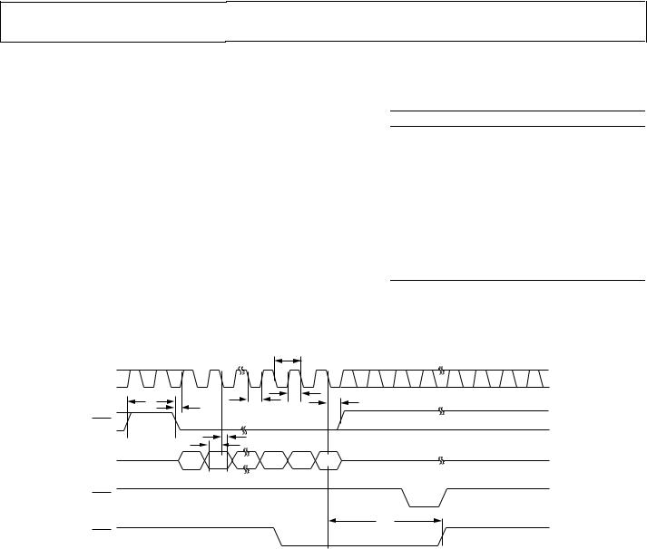
2 All input signals are specified with tr = tf = 5 ns (10% to 90% of VDD) and timed from a voltage level of (VIL + VIH)/2. 3 See Figure 2.
|
|
|
t1 |
SCLK |
|
|
|
t8 |
|
t3 |
t2 |
|
t7 |
||
|
|
t4 |
|
SYNC |
|
|
|
|
t6 |
t5 |
|
|
|
|
DIN1 |
DB15 |
DB0 |
 t9
t9 

LDAC
t10
LDAC
1SEE INPUT SHIFT REGISTER SECTION.
Figure 2. Serial Interface Timing Diagram
00928-002
Rev. D | Page 5 of 24
AD5302/AD5312/AD5322
|
GAIN ERROR |
|
|
PLUS |
|
|
OFFSET ERROR |
|
OUTPUT |
IDEAL |
|
VOLTAGE |
||
|
||
|
ACTUAL |
|
POSITIVE |
|
|
OFFSET |
DAC CODE |
|
ERROR |
|
DEADBAND
AMPLIFIER FOOTROOM
(1mV)
NEGATIVE
OFFSET
ERROR  004-02928
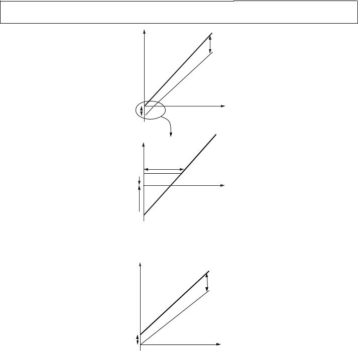
Figure 3. Transfer Function with Negative Offset
|
|
GAIN ERROR |
|
|
PLUS |
|
|
OFFSET ERROR |
OUTPUT |
ACTUAL |
|
VOLTAGE |
|
|
|
IDEAL |
|
POSITIVE |
|
|
OFFSET |
|
00928-005 |
ERROR |
|
|
|
DAC CODE |
|
|
|
Figure 4. Transfer Function with Positive Offset
Rev. D | Page 6 of 24

ABSOLUTE MAXIMUM RATINGS
TA = 25°C, unless otherwise noted.1
Table 4.
Parameter |
Rating |
|
|
VDD to GND |
–0.3 V to +7 V |
Digital Input Voltage to GND |
–0.3 V to VDD + 0.3 V |
Reference Input Voltage to |
–0.3 V to VDD + 0.3 V |
GND |
|
VOUTA, VOUTB to GND |
–0.3 V to VDD + 0.3 V |
Operating Temperature Range |
|
Industrial (A, B Version) |
–40°C to +105°C |
Storage Temperature Range |
–65°C to +150°C |
Junction Temperature (TJ max) |
+150°C |
10-Lead MSOP |
|
Power Dissipation |
(TJ max – TA)/θJA |
θJA Thermal Impedance |
206°C/W |
θJC Thermal Impedance |
44°C/W |
Lead Temperature, Soldering |
|
Vapor Phase (60 sec) |
215°C |
Infrared (15 sec) |
220°C |
1 Transient currents of up to 100 mA do not cause SCR latch-up.
AD5302/AD5312/AD5322
Stresses above those listed under Absolute Maximum Ratings may cause permanent damage to the device. This is a stress rating only; functional operation of the device at these or any other conditions above those indicated in the operational section of this specification is not implied. Exposure to absolute maximum rating conditions for extended periods may affect device reliability.
ESD CAUTION
ESD (electrostatic discharge) sensitive device. Electrostatic charges as high as 4000 V readily accumulate on the human body and test equipment and can discharge without detection. Although this product features proprietary ESD protection circuitry, permanent damage may occur on devices subjected to high energy electrostatic discharges. Therefore, proper ESD precautions are recommended to avoid performance degradation or loss of functionality.
Rev. D | Page 7 of 24
AD5302/AD5312/AD5322
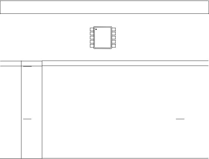
PIN CONFIGURATION AND FUNCTION DESCRIPTIONS
|
LDAC |
|
1 |
AD5302/ |
10 |
GND |
|||||
|
|
VDD |
2 |
AD5312/ |
9 |
DIN |
|||||
VREFB |
3 |
8 |
SCLK |
||||||||
AD5322 |
|||||||||||
VREFA |
4 |
TOP VIEW |
7 |
|
SYNC |
|
|||||
V |
OUT |
A |
5 |
(Not to Scale) |
6 |
V B |
|||||
|
|
|
|
|
|
|
|
OUT |
|||
00928-003
Figure 5. Pin Configuration
Table 5. Pin Function Descriptions
Pin No. |
Mnemonic |
1LDAC
2VDD
3VREFB
4VREFA
5VOUTA
6VOUTB
7SYNC
8SCLK
9DIN
10 GND
Description
Active Low Control Input. This pin transfers the contents of the input registers to their respective DAC registers. Pulsing LDAC low allows either or both DAC registers to be updated if the input registers have new data. This allows simultaneous updating of both DAC outputs.
Power Supply Input. The parts can be operated from 2.5 V to 5.5 V, and the supply should be decoupled to GND.
Reference Input Pin for DAC B. This is the reference for DAC B. It can be configured as a buffered or an unbuffered input, depending on the BUF bit in the control word of DAC B. It has an input range of 0 V to VDD in unbuffered mode and 1 V to VDD in buffered mode.
Reference Input Pin for DAC A. This is the reference for DAC A. It can be configured as a buffered or an unbuffered input depending on the BUF bit in the control word of DAC A. It has an input range of 0 V to VDD in unbuffered mode and 1 V to VDD in buffered mode.
Buffered Analog Output Voltage from DAC A. The output amplifier has rail-to-rail operation. Buffered Analog Output Voltage from DAC B. The output amplifier has rail-to-rail operation.
Active Low Control Input. This is the frame synchronization signal for the input data. When SYNC goes low, it powers on the SCLK and DIN buffers and enables the input shift register. Data is transferred in on the falling edges of the following 16 clocks. If SYNC is taken high before the 16th falling edge, the rising edge of SYNC acts as an interrupt and the write sequence is ignored by the device.
Serial Clock Input. Data is clocked into the input shift register on the falling edge of the serial clock input. Data can be transferred at rates up to 30 MHz. The SCLK input buffer is powered down after each write cycle.
Serial Data Input. This device has a 16-bit input shift register. Data is clocked into the register on the falling edge of the serial clock input. The DIN input buffer is powered down after each write cycle.
Ground Reference Point for All Circuitry on the Part.
Rev. D | Page 8 of 24
Loading...