


 Loading...
1-/2-Channel 15 V Digital Potentiometer
FEATURES
256 positions AD5260: 1 channel
AD5262: 2 channels (independently programmable) Potentiometer replacement
20 kΩ, 50 kΩ, 200 kΩ
Low temperature coefficient: 35 ppm/°C 4-wire, SPI-compatible serial data input
5 V to 15 V single-supply; ±5.5 V dual-supply operation Power on midscale preset
APPLICATIONS
Mechanical potentiometer replacement
Instrumentation: gain, offset adjustment
Stereo channel audio level control
Programmable voltage-to-current conversion
Programmable filters, delays, time constants
Line impedance matching
Low resolution DAC replacement
GENERAL DESCRIPTION
The AD5260/AD5262 provide a singleor dual-channel, 256position, digitally controlled variable resistor (VR) device.1 These devices perform the same electronic adjustment function as a potentiometer or variable resistor. Each channel of the AD5260/AD5262 contains a fixed resistor with a wiper contact that taps the fixed resistor value at a point determined by a digital code loaded into the SPI-compatible serial-input register. The resistance between the wiper and either end point of the fixed resistor varies linearly with respect to the digital code transferred into the VR latch. The variable resistor offers a completely programmable value of resistance, between the A terminal and the wiper or the B terminal and the wiper. The fixed A-to-B terminal resistance of 20 Ω, 50 Ω, or 200 Ω has a nominal temperature coefficient of 35 ppm/°C. Unlike the majority of the digital potentiometers in the market, these devices can operate up to 15 V or ±5 V provided proper supply voltages are furnished.
Each VR has its own VR latch that holds its programmed resistance value. These VR latches are updated from an internal serial-to-parallel shift register, which is loaded from a standard 3-wire serial-input digital interface. The AD5260 contains an 8-bit serial register whereas the AD5262 contains a 9-bit serial register. Each bit is clocked into the register on the positive
Rev. A
Information furnished by Analog Devices is believed to be accurate and reliable. However, no responsibilityisassumedbyAnalogDevicesforitsuse,norforanyinfringementsofpatentsorother rightsofthirdpartiesthatmayresultfromitsuse.Specificationssubjecttochangewithoutnotice.No license is granted by implication or otherwise under any patent or patent rights of Analog Devices. Trademarksandregisteredtrademarksarethepropertyoftheirrespectiveowners.
AD5260/AD5262
FUNCTIONAL BLOCK DIAGRAMS
|
A W B |
SHDN |
AD5260 |
|
VDD |
|
RDAC |
|
|
|
|
|
VSS |
REGISTER |
|
|
|
|
||
|
|
|
|
|
|
|
|
VL |
|
|
|
|
POWER-ON |
|
|
|
|
|
|
|
PR |
||
CS |
LOGIC |
|
|
|
RESET |
||
|
|
|
|
||||
|
|
|
|
8 |
|
|
|
CLK |
|
SERIAL INPUT REGISTER |
|
SDO |
|||
SDI |
|
|
|||||
|
|
|
|
|
|
001- |
|
GND |
|
|
|
|
|
|
02695 |
|
|
|
|
|
|
|
|
|
|
|
Figure 1. AD5260 |
|
|
|
|
|
A1 |
W1 |
B1 |
A2 |
W2 |
B2 |
|
SHDN |
|
|
|
|
|
|
|
VDD |
|
RDAC1 |
|
RDAC2 |
|
||
|
|
|
|
||||
VSS |
REGISTER |
REGISTER |
|
||||
VL |
|
|
|
|
|
|
|
CS |
LOGIC |
|
|
|
POWER-ON |
PR |
|
|
|
|
RESET |
|
|||
|
|
|
|
8 |
|
|
|
CLK |
|
SERIAL INPUT REGISTER |
|
SDO |
|||
SDI |
|
|
|||||
|
|
|
|
|
|
002- |
|
|
|
|
|
AD5262 |
|
|
|
GND |
|
|
|
|
|
02695 |
|
|
|
|
|
|
|
|
|
|
|
|
Figure 2. AD5262 |
|
|
|
|
edge of the CLK pin. The AD5262 address bit determines the corresponding VR latch to be loaded with the last eight bits of the data word during the positive edging of CS strobe. A serial data output pin at the opposite end of the serial register enables simple daisy-chaining in multiple VR applications without additional external decoding logic. An optional reset pin (PR) forces the wiper to the midscale position by loading 0x80 into the VR latch.
The AD5260/AD5262 are available in thin surface-mount 14-lead TSSOP and 16-lead TSSOP packages. All parts are guaranteed to operate over the extended industrial temperature range of −40°C to +85°C.
1 The terms digital potentiometers, VR, and RDAC are used interchangeably.
One Technology Way, P.O. Box 9106, Norwood, MA 02062-9106, U.S.A. Tel: 781.329.4700 www.analog.com Fax: 781.461.3113 ©2002–2010 Analog Devices, Inc. All rights reserved.

AD5260/AD5262
TABLE OF CONTENTS |
|
|
Features .............................................................................................. |
|
1 |
Applications....................................................................................... |
|
1 |
General Description ......................................................................... |
|
1 |
Functional Block Diagrams............................................................. |
|
1 |
Revision History ............................................................................... |
|
2 |
Specifications..................................................................................... |
|
3 |
Electrical Characteristics—20 kΩ, 50 kΩ, 200 kΩ Versions |
.. 3 |
|
Timing Diagrams.......................................................................... |
|
5 |
Absolute Maximum Ratings............................................................ |
|
6 |
ESD Caution.................................................................................. |
|
6 |
Pin Configurations and Function Descriptions ........................... |
|
7 |
Typical Performance Characteristics ............................................. |
|
9 |
Test Circuits..................................................................................... |
|
14 |
Theory of Operation ...................................................................... |
|
15 |
Digital Interfacing ...................................................................... |
|
15 |
Daisy-Chain Operation ............................................................. |
|
16 |
RDAC Structure.......................................................................... |
|
16 |
Programming the Variable Resistor......................................... |
|
16 |
Programming the Potentiometer Divider ............................... |
|
17 |
REVISION HISTORY |
|
|
8/10—Rev. 0 to Rev. A |
|
|
Updated Format.................................................................. |
Universal |
|
Deleted Figure 1; Renumbered Sequentially................................. |
|
1 |
Changes to General Description Section ...................................... |
|
1 |
Changes to Conditions of Channel Resistance Matching |
|
|
(AD5262 only) Parameter, Voltage Divider Temperature |
|
|
Coefficient Parameter, Full-Scale Error Parameter, and Zero- |
|
|
Scale Error Parameter, Table 1 ........................................................ |
|
3 |
Changes to Table 2 and Table 3....................................................... |
|
5 |
Changes to Table 4............................................................................ |
|
6 |
Changes to Table 5............................................................................ |
|
7 |
Changes to Table 6............................................................................ |
|
8 |
Layout and Power Supply Bypassing ....................................... |
18 |
Terminal Voltage Operating Range ......................................... |
18 |
Power-Up Sequence ................................................................... |
18 |
RDAC Circuit Simulation Model............................................. |
18 |
Macro Model Net List for RDAC ............................................. |
18 |
Applications Information .............................................................. |
19 |
Bipolar DC or AC Operation from Dual Supplies................. |
19 |
Gain Control Compensation .................................................... |
19 |
Programmable Voltage Reference............................................ |
19 |
8-Bit Bipolar DAC ...................................................................... |
19 |
Bipolar Programmable Gain Amplifier................................... |
20 |
Programmable Voltage Source with Boosted Output ........... |
20 |
Programmable 4 mA-to-20 mA Current Source ................... |
20 |
Programmable Bidirectional Current Source......................... |
21 |
Programmable Low-Pass Filter ................................................ |
21 |
Programmable Oscillator .......................................................... |
21 |
Resistance Scaling ...................................................................... |
22 |
Outline Dimensions ....................................................................... |
23 |
Ordering Guide .......................................................................... |
24 |
Changes to Figure 11 Caption and Figure 12 ................................ |
9 |
Changes to Figure 31...................................................................... |
12 |
Changes to Figure 35 Caption ...................................................... |
13 |
Changes to Figure 43 and Figure 46............................................. |
14 |
Deleted Potentiometer Family Selection Guide ......................... |
18 |
Change to Programmable Voltage Source with Boosted Output |
|
Section.............................................................................................. |
20 |
Changes to Figure 64...................................................................... |
21 |
Updated Outline Dimensions....................................................... |
23 |
Changes to Ordering Guide .......................................................... |
24 |
3/02—Revision 0: Initial Version |
|
Rev. A | Page 2 of 24

AD5260/AD5262
SPECIFICATIONS
ELECTRICAL CHARACTERISTICS—20 kΩ, 50 kΩ, 200 kΩ VERSIONS
VDD = +15 V, VSS = 0 V, or VDD = +5 V, VSS = –5 V; VL = +5 V; VA = +5 V, VB = 0 V, −40°C < TA < +85°C, unless otherwise noted. The AD5260/AD5262 contain 1968 transistors. Die size: 89 mil × 105 mil (9345 sq mil).
Table 1.
Parameter |
Symbol |
Conditions |
Min |
Typ1 |
Max |
Unit |
DC CHARACTERISTICS RHEOSTAT MODE |
|
Specifications apply to all VRs |
|
|
|
|
Resistor Differential Nonlinearity2 |
R-DNL |
RWB, VA = no connect |
−1 |
±¼ |
+1 |
LSB |
Resistor Nonlinearity2 |
R-INL |
RWB, VA = no connect |
−1 |
±½ |
+1 |
LSB |
Nominal Resistor Tolerance3 |
ΔRAB |
TA = 25°C |
−30 |
|
30 |
% |
Resistance Temperature Coefficient |
ΔRAB/ΔT |
Wiper = no connect |
|
35 |
|
ppm/°C |
Wiper Resistance |
RW |
IW = 1 V/RAB |
|
60 |
150 |
Ω |
Channel Resistance Matching (AD5262 only) |
ΔRWB/RWB |
Channel 1 and Channel 2 RWB, |
|
0.1 |
|
% |
|
|
DX = 0x80 |
|
|
|
|
Resistance Drift |
ΔRAB |
|
|
0.05 |
|
% |
|
|
|
|
|
|
|
DC CHARACTERISTICS POTENTIOMETER DIVIDER MODE |
|
Specifications apply to all VRs |
|
|
|
|
Resolution |
N |
|
8 |
|
|
Bits |
Differential Nonlinearity4 |
DNL |
|
−1 |
±1/4 |
+1 |
LSB |
Integral Nonlinearity4 |
INL |
|
−1 |
±1/2 |
+1 |
LSB |
Voltage Divider Temperature Coefficient |
ΔVW/ΔT |
Code = half scale |
|
5 |
|
ppm/°C |
Full-Scale Error |
WFSE |
Code = full scale |
−2 |
−1 |
+0 |
LSB |
Zero-Scale Error |
VWZSE |
Code = zero scale |
0 |
1 |
2 |
LSB |
|
|
|
|
|
|
|
RESISTOR TERMINALS |
|
|
|
|
|
|
Voltage Range5 |
VA, B, W |
|
VSS |
|
VDD |
V |
Ax and Bx Capacitance6 |
CA,B |
f = 5 MHz, measured to GND, |
|
25 |
|
pF |
|
|
code = half scale |
|
|
|
|
Wx Capacitance6 |
CW |
f = 1 MHz, measured to GND, |
|
55 |
|
pF |
|
|
code = half scale |
|
|
|
|
Common-Mode Leakage Current |
ICM |
VA = VB = VDD/2 |
|
1 |
|
nA |
Shutdown Current7 |
ISHDN |
|
|
|
5 |
μA |
DIGITAL INPUTS and OUTPUTS |
|
|
|
|
|
|
Input Logic High |
VIH |
|
2.4 |
|
|
V |
Input Logic Low |
VIL |
|
|
|
0.8 |
V |
Input Logic High |
VIH |
VL = 3 V, VSS = 0 V |
2.1 |
|
|
V |
Input Logic Low |
VIL |
VL = 3 V, VSS = 0 V |
|
|
0.6 |
V |
Output Logic High (SDO) |
VOH |
RPULL-UP = 2 kΩ to 5 V |
4.9 |
|
|
V |
Output Logic Low (SDO) |
VOL |
IOL = 1.6 mA, VLOGIC = 5 V |
|
|
0.4 |
V |
Input Current8 |
IIL |
VIN = 0 V or 5 V |
|
|
±1 |
μA |
Input Capacitance6 |
CIL |
|
|
5 |
|
pF |
POWER SUPPLIES |
|
|
|
|
|
|
Logic Supply |
VL |
|
2.7 |
|
5.5 |
V |
Power Single-Supply Range |
VDD RANGE |
VSS = 0 V |
4.5 |
|
16.5 |
V |
Power Dual-Supply Range |
VDD/SS RANGE |
|
±4.5 |
|
±5.5 |
V |
Logic Supply Current |
IL |
VL = 5 V |
|
|
60 |
μA |
Positive Supply Current |
IDD |
VIH = 5 V or VIL = 0 V |
|
|
1 |
μA |
Negative Supply Current |
ISS |
VSS= −5 V |
|
|
1 |
μA |
Power Dissipation9 |
PDISS |
VIH = 5 V or VIL = 0 V, |
|
|
0.3 |
mW |
|
|
VDD = +5 V, VSS = –5 V |
|
|
|
|
Power Supply Sensitivity |
PSS |
ΔVDD= +5 V, ±10% |
|
0.003 |
0.01 |
%/% |
|
|
|
|
|
|
|
Rev. A | Page 3 of 24

AD5260/AD5262
Parameter |
Symbol |
Conditions |
Min Typ1 |
Max |
Unit |
||||
DYNAMIC CHARACTERISTICS6, 10 |
|
|
|
|
|
||||
|
Bandwidth –3 dB |
BW |
RAB = 20 kΩ/50 kΩ/200 kΩ |
310/130/30 |
|
kHz |
|||
|
Total Harmonic Distortion |
THDW |
VA = 1 VRMS, VB = 0 V, f = 1 kHz, |
0.014 |
|
% |
|||
|
|
|
|
|
|
RAB = 20 kΩ |
|
|
|
|
VW Settling Time |
tS |
VA = +5 V, VB = −5 V, ±1 LSB |
5 |
|
μs |
|||
|
|
|
|
|
|
error band, RAB = 20 kΩ |
|
|
|
|
Crosstalk11 |
CT |
VA = VDD, VB = 0 V, measure VW |
1 |
|
nV-sec |
|||
|
|
|
|
|
|
with adjacent RDAC making |
|
|
|
|
|
|
|
|
|
full-scale code change (AD5262 |
|
|
|
|
|
|
|
|
|
only) |
|
|
|
|
Analog Crosstalk |
CTA |
VA1 = VDD, VB1 = 0 V, measure VW1 |
–64 |
|
dB |
|||
|
|
|
|
|
|
with VW2 = 5 V p-p at f = 10 kHz, |
|
|
|
|
|
|
|
|
|
RAB = 20 kΩ/200 kΩ (AD5262 |
|
|
|
|
|
|
|
|
|
only) |
|
|
|
|
Resistor Noise Voltage |
eN_WB |
RWB = 20 kΩ, f = 1 kHz |
13 |
|
nV/√Hz |
|||
INTERFACE TIMING CHARACTERISTICS6, 12 |
|
Specifications apply to all parts |
|
|
|
||||
|
Clock Frequency |
fCLK |
|
|
25 |
MHz |
|||
|
Input Clock Pulse Width |
tCH, tCL |
Clock level high or low |
20 |
|
ns |
|||
|
Data Setup Time |
tDS |
|
10 |
|
ns |
|||
|
Data Hold Time |
tDH |
|
10 |
|
ns |
|||
|
CLK to SDO Propagation Delay13 |
tPD |
RL = 1 kΩ, CL< 20 pF |
1 |
160 |
ns |
|||
|
CS |
Setup Time |
tCSS |
|
5 |
|
ns |
||
|
|
|
|
tCSW |
|
20 |
|
ns |
|
|
CS |
High Pulse Width |
|
|
|||||
|
Reset Pulse Width |
tRS |
|
50 |
|
ns |
|||
|
|
tCSH |
|
0 |
|
ns |
|||
|
CLK Fall to |
CS |
Rise Hold Time |
|
|
||||
|
|
tCS1 |
|
10 |
|
ns |
|||
|
CS |
Rise to Clock Rise Setup |
|
|
|||||
1 Typical values represent average readings at 25°C and VDD = +5 V, VSS = −5 V.
2Resistor position nonlinearity error (R-INL) is the deviation from an ideal value measured between the maximum resistance and the minimum resistance wiper positions. R-DNL measures the relative step change from ideal between successive tap positions. Parts are guaranteed monotonic. IW = VDD/R for both VDD = +5 V and
VSS = −5V.
3 VAB = VDD, wiper = no connect.
4INL and DNL are measured at VW with the RDAC configured as a potentiometer divider similar to a voltage output digital-to-analog converter. VA = VDD and VB = 0 V. DNL specification limits of ±1 LSB maximum are guaranteed monotonic operating conditions.
5 Resistor Terminal A, Terminal B, and Terminal W have no limitations on polarity with respect to each other. 6 Guaranteed by design and not subject to production test.
7 Measured at the Ax terminals. All Ax terminals are open-circuit in shutdown mode.
8 Worst-case supply current consumed when all logic-input levels set at 2.4 V, which is the standard characteristic of CMOS logic. 9 PDISS is calculated from (IDD × VDD). CMOS logic level inputs result in minimum power dissipation.
10All dynamic characteristics use VDD = +5 V, VSS = −5 V, VL = +5 V.
11Measured at VW where an adjacent VW is making a full-scale voltage change.
12See Figure 5 for location of measured values. All input control voltages are specified with tR = tF = 2 ns (10% to 90% of 3 V) and timed from a voltage level of 1.5 V. Switching characteristics are measured using VL = 5 V.
13Propagation delay depends on value of VDD, RL, and CL.
Rev. A | Page 4 of 24
|
|
|
|
|
|
|
|
|
|
|
|
|
|
AD5260/AD5262 |
||
|
|
|
|
|
|
|
|
|
|
|
|
|
|
|
|
|
TIMING DIAGRAMS |
|
|
|
|
|
|
|
|
|
|
|
|
|
|
||
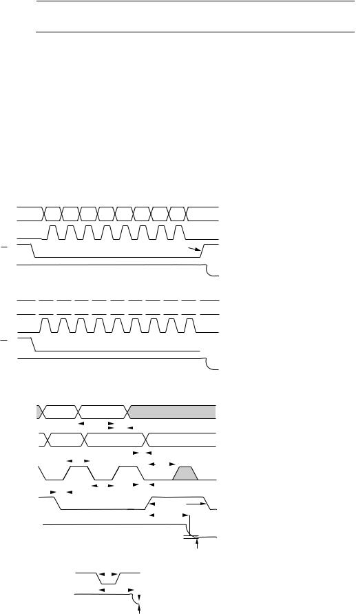
Table 2. AD5260 8-Bit Serial Data Word Format |
|
|
|
|
|
|
|
|
|
|
|
|
||||
|
|
|
|
|
|
|
Data |
|
|
|
|
|
|
|
|
|
B7 (MSB) |
|
B6 |
B5 |
|
B4 |
|
B3 |
|
|
B2 |
B1 |
|
B0 (LSB) |
|||
D7 |
|
D6 |
D5 |
|
D4 |
|
D3 |
|
|
D2 |
D1 |
|
D0 |
|||
27 |
|
26 |
25 |
|
|
24 |
|
23 |
|
|
22 |
|
21 |
|
20 |
|
Table 3. AD5262 9-Bit Serial Data Word Format |
|
|
|
|
|
|
|
|
|
|
|
|
||||
ADDR |
|
|
|
|
|
|
|
|
Data |
|
|
|
|
|
|
|
B8 |
B7 (MSB) |
B6 |
B5 |
B4 |
|
B3 |
|
B2 |
|
B1 |
|
B0 (LSB) |
||||
A0 |
D7 |
D6 |
D5 |
D4 |
|
D3 |
|
D2 |
|
D1 |
|
D0 |
||||
28 |
27 |
26 |
|
25 |
24 |
|
|
23 |
|
22 |
|
21 |
|
20 |
||
|
1 |
|
|
|
|
|
|
|
SDI |
D7 |
D6 |
D5 |
D4 |
D3 |
D2 |
D1 |
D0 |
|
0 |
|
|
|
|
|
|
|
CLK |
1 |
|
|
|
|
|
|
|
0 |
|
|
|
|
|
|
|
|
|
|
|
|
|
|
|
|
|
CS |
1 |
|
|
|
RDAC REGISTER LOAD |
|||
|
|
|
|
|||||
0 |
|
|
|
|
|
|
|
|
|
|
|
|
|
|
|
|
|
VOUT |
1 |
|
|
|
|
|
|
|
0 |
|
|
|
|
|
|
|
|
|
|
|
|
|
|
|
|
|
02695-004
Figure 3. AD5260 Timing Diagram
1
SDI
0
1
CLK
0
1
CS
0
1
VOUT
0
 A0
A0  D7
D7  D6
D6  D5
D5  D4
D4  D3
D3  D2
D2  D1
D1  D0
D0 
RDAC REGISTER LOAD 

02695-005
Figure 4. AD5262 Timing Diagram
SDI |
1 |
|
|
|
|
|
|
|
|
|
|
|
|
|
Dx |
|
|
|
|
|
|
|
|
|
|
|
|
|
|
||||||
|
|
|
|
|
|
|
|
|
|
|
|
|
|
|
|||||||||||||||||||||
(DATA IN) |
Ax OR Dx |
|
|
|
|
|
|
|
|
|
|
|
|
|
|
|
|
|
|
|
|||||||||||||||
0 |
|
|
|
|
|
|
|
|
|
|
|
|
|
tDS |
|
|
|
|
|
|
|
|
|
|
|
|
|
|
|
|
|
|
|||
SDO |
1 |
|
|
|
|
|
|
|
|
|
|
|
|
|
|
|
|
|
tDH |
|
|
|
|
|
|
|
|
|
|
|
|
|
|||
|
A'x OR D'x |
|
D'x |
|
|
|
|
|
|
|
|
|
|
|
|
||||||||||||||||||||
|
|
|
|
|
|
|
|
|
|
|
|
|
|
|
|
||||||||||||||||||||
(DATA OUT) |
0 |
|
|
|
|
|
|
|
|
|
|
|
|
|
|
|
|
||||||||||||||||||
|
|
|
|
|
|
|
|
|
|
|
|
|
|
|
|
|
|
|
|
|
|
|
|
|
|
|
|
|
|
|
|
||||
|
|
|
|
|
|
|
|
|
|
tCH |
|
|
|
|
|
|
|
|
|
|
|
|
|
|
tPD |
||||||||||
|
|
|
|
|
|
|
|
|
|
|
|
|
|
|
|
|
|
|
|
|
|
|
|
||||||||||||
CLK |
1 |
|
|
|
|
|
|
|
|
|
|
|
|
|
|
|
|
|
|
|
|
tCS1 |
|
|
|
|
|||||||||
|
|
|
|
|
|
|
|
|
|
|
|
|
|
|
|
|
|
|
|
|
|
|
|
|
|
|
|
|
|||||||
|
|
|
0 |
|
|
|
|
|
|
|
tCSS |
tCL |
|
|
|
|
|
|
|
|
tCSH |
||||||||||||||
|
|
|
1 |
|
|
|
|
|
|
|
|
|
|
|
|
|
|
|
|||||||||||||||||
|
|
|
|
|
|
|
|
|
|
|
|
|
|
|
|
|
|
||||||||||||||||||
|
|
|
|
|
|
|
|
|
|
|
|
|
|
|
|||||||||||||||||||||
|
|
|
|
|
|
|
|
|
|
|
|
|
|
|
|
|
|
|
|
|
|
|
|
|
|
tCSW |
|||||||||
|
|
|
|
|
|
|
|
|
|
|
|
|
|
|
|
|
|
|
|
|
|
|
|
|
|
|
|
|
|
|
|
||||
|
CS |
|
0 |
|
|
|
|
|
|
|
|
|
|
|
|
|
|
|
|
|
|
|
|
|
|
|
|
|
|
|
|
|
|||
|
|
|
|
|
|
|
|
|
|
|
|
|
|
|
|
|
|
|
|
|
|
|
|
|
|
|
|
|
|||||||
|
|
|
|
|
|
|
|
|
|
|
|
|
|
|
|
|
|
|
|
|
|
|
|
|
|
|
|
|
|
tS |
|
|
|||
VOUT |
VDD |
|
|
|
|
|
|
|
|
|
|
|
|
|
|
|
|||||||||||||||||||
|
|
|
|
|
|
|
|
|
|
|
|
|
|
|
|
|
|
|
|||||||||||||||||
|
|
|
|
|
|
|
|
|
|
|
|
|
|
|
|
|
|
|
±1 LSB ERROR BRAND |
||||||||||||||||
|
|
|
0V |
|
|
|
|
|
|||||||||||||||||||||||||||
Figure 5. Detailed Timing Diagram
 ±1 LSB
02695-006
|
|
1 |
|
|
tRS |
|
|
|
|
|
|
|
|
|
||
|
|
|
|
|
|
|
||||||||||
|
PR |
|
|
|
|
|
|
|
|
|
|
|
|
|
|
|
0 |
|
|
|
|
tS |
|
|
|
|
|
|
|
||||
|
|
VDD |
|
|
|
|
|
|
|
|
±1 LSBD |
|||||
|
|
|
|
|
|
|
|
|
|
|
|
|
|
|||
|
|
0V ±1 LSB ERROR BAND |
|
|
|
|
|
|||||||||
|
|
|
|
|
||||||||||||
Figure 6. Preset Timing Diagram
02695-007
Rev. A | Page 5 of 24
AD5260/AD5262
ABSOLUTE MAXIMUM RATINGS
TA =25°C, unless otherwise noted.
Table 4.
Parameter |
Rating |
|
|
VDD to GND |
−0.3 V to +17 V |
VSS to GND |
0 V to −7 V |
VDD to VSS |
17 V |
VL to GND |
0 V to +7 V |
VA, VB, VW to GND |
VSS, VDD |
AX to BX, AX to WX, BX to WX |
|
Intermittent1 |
±20 mA |
Continuous |
±5 mA |
Digital Inputs and Output Voltage |
−0.3 V to VL + 0.3 V, or |
to GND |
+7 V (whichever is less) |
Operating Temperature Range |
−40°C to +85°C |
Maximum Junction Temperature |
150°C |
(TJ MAX) |
|
Storage Temperature Range |
−65°C to +150°C |
Lead Temperature (Soldering,10 sec) |
300°C |
Vapor Phase (60 sec) |
215°C |
Infrared (15 sec) |
220°C |
Thermal Resistance2 θJA |
|
14-Lead TSSOP |
206°C/W |
16-Lead TSSOP |
150°C/W |
|
|
Stresses above those listed under Absolute Maximum Ratings may cause permanent damage to the device. This is a stress rating only; functional operation of the device at these or any other conditions above those indicated in the operational section of this specification is not implied. Exposure to absolute maximum rating conditions for extended periods may affect device reliability.
ESD CAUTION
1Maximum terminal current is bounded by the maximum current handling of the switches, maximum power dissipation of the package, and maximum applied voltage across any two of the A, B, and W terminals at a given resistance setting.
2 Package power dissipation = (TJ MAX − TA)/θJA.
Rev. A | Page 6 of 24
AD5260/AD5262
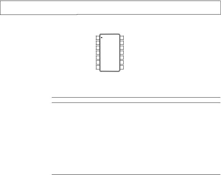
PIN CONFIGURATIONS AND FUNCTION DESCRIPTIONS
A |
1 |
|
14 |
SDO |
|||||
W |
2 |
|
13 |
|
NC |
||||
B |
3 |
AD5260 |
12 |
|
VL |
||||
VDD |
4 |
TOP VIEW |
11 |
|
VSS |
||||
(Not to Scale) |
|
||||||||
SHDN |
|
5 |
|
10 |
|
GND |
|||
CLK |
6 |
|
9 |
|
|
|
|
|
|
|
PR |
||||||||
SDI |
7 |
|
8 |
|
|
|
|||
|
|
CS |
|||||||
NC = NO CONNECT
02695-008
Figure 7. AD5260 Pin Configuration
Table 5. AD5260 Pin Function Descriptions
Pin No. |
|
Mnemonic |
Description |
|||||
1 |
|
A |
A Terminal. |
|||||
2 |
W |
Wiper Terminal. |
||||||
3 |
B |
B Terminal. |
||||||
4 |
|
VDD |
Positive Power Supply. Specified for operation at both 5 V or 15 V (sum of |VDD| + |VSS| ≤ 15 V). |
|||||
5 |
|
|
|
|
Active Low Input. Terminal A, open-circuit. Shutdown controls variable resistor. |
|||
|
SHDN |
|
||||||
6 |
|
CLK |
Serial Clock Input, Positive Edge Triggered. |
|||||
7 |
|
SDI |
Serial Data Input. |
|||||
8 |
|
|
|
Chip Select Input, Active Low. When |
|
returns high, data is loaded into the RDAC register. |
||
|
CS |
|
CS |
|||||
9 |
|
|
Active Low Preset to Midscale. Sets RDAC registers to 0x80. |
|||||
|
PR |
|
||||||
10 |
|
GND |
Ground. |
|||||
11 |
|
VSS |
Negative Power Supply. Specified for operation from 0 V to −5 V. |
|||||
12 |
|
VL |
Logic Supply Voltage. Needs to be the same voltage as the digital logic controlling the AD5260. |
|||||
13 |
NC |
No Connect. Users should not connect anything other than a dummy pad on this pin. |
||||||
14 |
SDO |
Serial Data Output. Open-drain transistor requires a pull-up resistor. |
||||||
Rev. A | Page 7 of 24
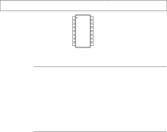
AD5260/AD5262
SDO |
1 |
16 |
A2 |
A1 |
2 |
15 |
W2 |
|
W1 |
3 |
AD5262 |
14 |
B2 |
||||
|
B1 |
4 |
TOP VIEW |
13 |
VL |
||||
|
VDD |
5 |
(Not to Scale) |
12 |
VSS |
||||
|
|
||||||||
|
SHDN |
|
6 |
|
11 |
GND |
|||
|
CLK |
7 |
|
10 |
|
|
|
|
|
|
|
PR |
|||||||
|
SDI |
8 |
|
9 |
|
|
|||
|
|
CS |
|||||||
02695-009
|
|
|
|
|
|
Figure 8. AD5262 Pin Configuration |
||
Table 6. AD5262 Pin Function Descriptions |
||||||||
Pin No. |
|
Mnemonic |
Description |
|||||
|
|
|
|
|
|
|
|
|
1 |
SDO |
Serial Data Output. Open-drain transistor requires a pull-up resistor. |
||||||
2 |
|
A1 |
A Terminal RDAC 1. |
|||||
3 |
W1 |
Wiper RDAC 1, Address A0 = 0. |
||||||
4 |
B1 |
B Terminal RDAC 1. |
||||||
5 |
|
VDD |
Positive Power Supply. Specified for operation at both 5 V or 15 V. (Sum of |VDD| + |VSS| ≤ 15 V) |
|||||
6 |
|
|
|
|
Active Low Input. Terminal A, open-circuit. Shutdown controls variable Resistor 1 through Resistor R2. |
|||
|
SHDN |
|
||||||
7 |
CLK |
Serial Clock Input, Positive Edge Triggered. |
||||||
8 |
SDI |
Serial Data Input. |
||||||
9 |
|
|
|
Chip Select Input, Active Low. When |
|
returns high, data in the serial input register is decoded, based on the |
||
|
CS |
|
CS |
|||||
|
|
|
|
|
|
Address Bit A0, and loaded into the target RDAC register. |
||
10 |
|
|
Active Low Preset to Midscale. Sets RDAC registers to 0x80. |
|||||
|
PR |
|
||||||
11 |
GND |
Ground. |
||||||
12 |
|
VSS |
Negative Power Supply. Specified for operation at either 0 V or −5 V (sum of |VDD| + |VSS| < 15 V). |
|||||
13 |
|
VL |
Logic Supply Voltage. Needs to be same voltage as the digital logic controlling the AD5262. |
|||||
14 |
B2 |
B Terminal RDAC 2. |
||||||
15 |
W2 |
Wiper RDAC 2, Address A0 = 1. |
||||||
16 |
|
A2 |
A Terminal RDAC 2. |
|||||
|
|
|
|
|
|
|
|
|
Rev. A | Page 8 of 24
Loading...