


AD5330
Table of contents
 Loading...
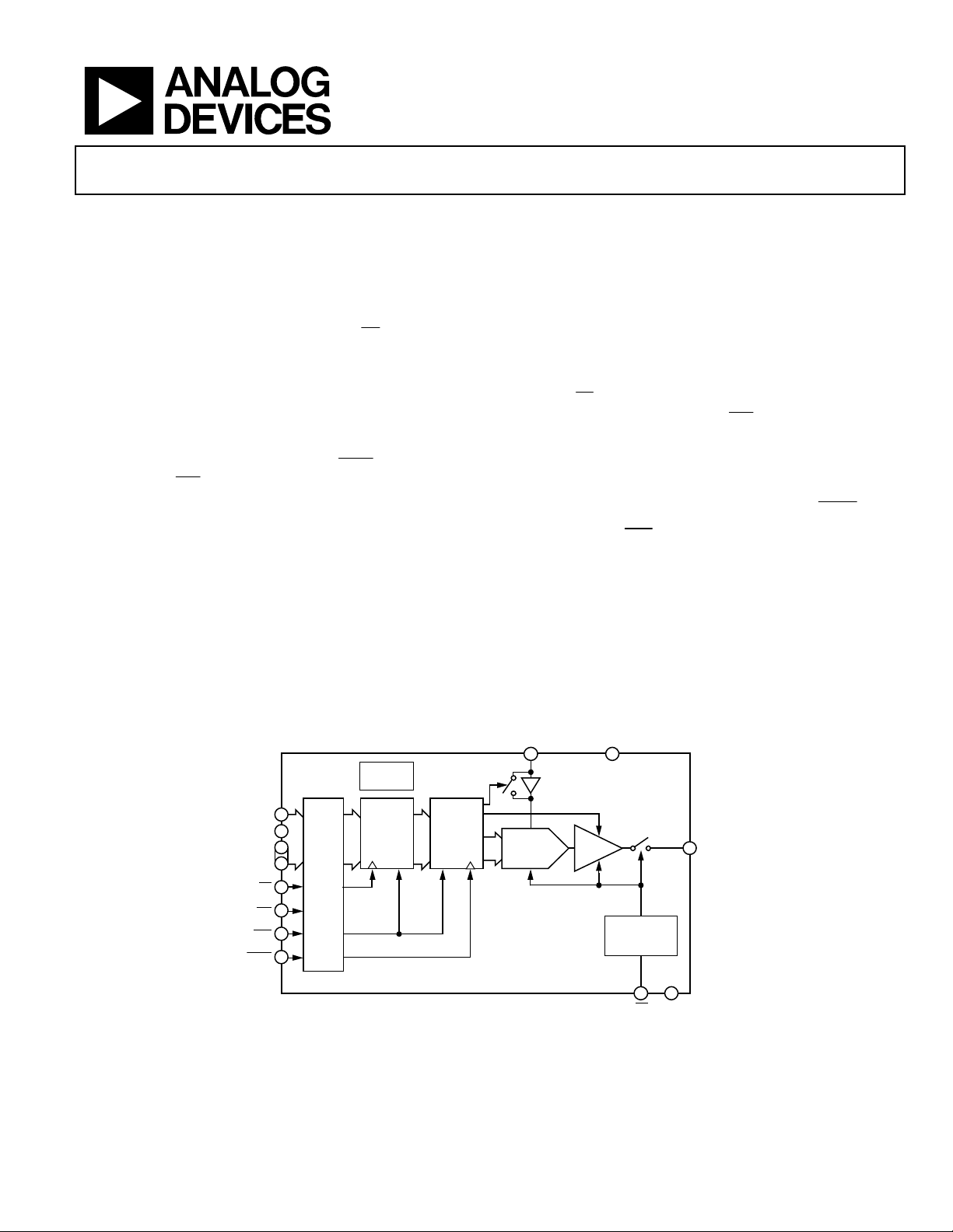
2.5 V to 5.5 V, 115 μA, Parallel Interface
Single Voltage-Output 8-/10-/12-Bit DACs
AD5330/AD5331/AD5340/AD5341
Rev. A
Information furnished by Analog Devices is believed to be accurate and reliable. However, no
responsibility is assumed by Analog Devices for its use, nor for any infringements of patents or other
rights of third parties that may result from its use. Specifications subject to change without notice. No
license is granted by implication or otherwise under any patent or patent rights of Analog Devices.
Trademarks and registered trademarks are the property of their respective owners.
One Technology Way, P.O. Box 9106, Norwood, MA 02062-9106, U.S.A.
Tel: 781.329.4700 www.analog.com
Fax: 781.461.3113 ©2000–2008 Analog Devices, Inc. All rights reserved.
FEATURES
AD5330: single 8-bit DAC in 20-lead TSSOP
AD5331: single 10-bit DAC in 20-lead TSSOP
AD5340: single 12-bit DAC in 24-lead TSSOP
AD5341: single 12-bit DAC in 20-lead TSSOP
Low power operation: 115 μA @ 3 V, 140 μA @ 5 V
Power-down to 80 nA @ 3 V, 200 nA @ 5 V via
PD
Pin
2.5 V to 5.5 V power supply
Double-buffered input logic
Guaranteed monotonic by design over all codes
Buffered/unbuffered reference input options
Output range: 0 V to V
REF
or 0 V to 2 × V
REF
Power-on reset to 0 V
Simultaneous update of DAC outputs via
LDAC
pin
Asynchronous
CLR
facility
Low power parallel data interface
On-chip rail-to-rail output buffer amplifiers
Temperature range: −40°C to +105°C
APPLICATIONS
Portable battery-powered instruments
Digital gain and offset adjustment
Programmable voltage and current sources
Programmable attenuators
Industrial process control
GENERAL DESCRIPTION
The AD5330/AD5331/AD5340/AD5341
1
are single 8-/10-/12-
bit DACs. They operate from a 2.5 V to 5.5 V supply consuming
just 115 μA at 3 V and feature a power-down mode that further
reduces the current to 80 nA. The devices incorporate an on-chip
output buffer that can drive the output to both supply rails, but
the AD5330, AD5340, and AD5341 allow a choice of buffered
or unbuffered reference input.
The AD5330/AD5331/AD5340/AD5341 have a parallel
interface.
CS
selects the device and data is loaded into the
input registers on the rising edge of
WR
.
The GAIN pin allows the output range to be set at 0 V to V
REF
or
0 V to 2 × V
REF
.
Input data to the DACs is double-buffered, allowing simultane-
ous update of multiple DACs in a system using the
LDAC
pin.
An asynchronous
CLR
input is also provided, which resets the
contents of the input register and the DAC register to all zeros.
These devices also incorporate a power-on reset circuit that
ensures that the DAC output powers on to 0 V and remains
there until valid data is written to the device.
The AD5330/AD5331/AD5340/AD5341 are available in thin
shrink small outline packages (TSSOP).
1
Protected by U.S. Patent Number 5,969,657.
FUNCTIONAL BLOCK DIAGRAM
BUFFER
8-BIT
DAC
DAC
REGISTER
INPUT
REGISTER
INTERFACE LOGIC
POWER-DOWN
LOGIC
BUF
GAIN
DB
7
DB
0
.
.
CS
WR
CLR
LDAC
V
REF
V
DD
V
OUT
PD GND
AD5330
POWER-ON
RESET
RESET
10
9
7
6
13
20
8
1
3 12
4
11 5
6852-001
Figure 1. AD5330

AD5330/AD5331/AD5340/AD5341
Rev. A | Page 2 of 28
TABLE OF CONTENTS
Features .............................................................................................. 1
Applications ....................................................................................... 1
General Description ......................................................................... 1
Functional Block Diagram .............................................................. 1
Revision History ............................................................................... 2
Specifications ..................................................................................... 3
AC Characteristics ........................................................................ 4
Timing Characteristics ................................................................ 5
Absolute Maximum Ratings ............................................................ 6
ESD Caution .................................................................................. 6
Pin Configurations and Function Descriptions ........................... 7
Terminology .................................................................................... 11
Typical Performance Characteristics ........................................... 13
Theory of Operation ...................................................................... 17
Digital-to-Analog Section ......................................................... 17
Resistor String ............................................................................. 17
DAC Reference Input ................................................................. 17
Output Amplifier ........................................................................ 17
Parallel Interface ............................................................................. 18
Double-Buffered Interface ........................................................ 18
Clear Input (
CLR
) ...................................................................... 18
Chip Select Input (
CS
) ............................................................... 18
Writ e I np u t (
WR
) ....................................................................... 18
Load DAC Input (
LDAC
) .......................................................... 18
High-Byte Enable Input (HBEN) ............................................. 18
Power-On Reset .......................................................................... 18
Power-Down Mode ........................................................................ 19
Suggested Databus Formats .......................................................... 20
Applications Information .............................................................. 21
Typical Application Circuits ..................................................... 21
Driving V
DD
From the Reference Voltage ............................... 21
Bipolar Operation Using the AD5330/AD5331/
AD5340/AD5341 ......................................................................... 21
Decoding Multiple AD5330/AD5331/ AD5340/AD5341 .... 21
Programmable Current Source ................................................ 22
Power Supply Bypassing and Grounding ................................ 22
Outline Dimensions ....................................................................... 24
Ordering Guide .......................................................................... 25
REVISION HISTORY
2/08—Rev. 0 to Rev. A
Updated Format .................................................................. Universal
Changes to Table 4 .......................................................................... 16
Replaced Driving V
DD
from the Reference Voltage Section ..... 21
Updated Outline Dimensions ....................................................... 24
Changes to Ordering Guide .......................................................... 25
4/00—Revision 0: Initial Version

AD5330/AD5331/AD5340/AD5341
Rev. A | Page 3 of 28
SPECIFICATIONS
V
DD
= 2.5 V to 5.5 V, V
REF
= 2 V, R
L
= 2 kΩ to GND; C
L
= 200 pF to GND; all specifications T
MIN
to T
MAX
, unless otherwise noted.
Table 1.
Parameter
1
B Version
2
Unit Conditions/Comments Min Typ Max
DC PERFORMANCE
3, 4
AD5330
Resolution 8 Bits
Relative Accuracy ±0.15 ±1 LSB
Differential Nonlinearity ±0.02 ±0.25 LSB Guaranteed monotonic by design over all codes
AD5331
Resolution 10 Bits
Relative Accuracy ±0.5 ±4 LSB
Differential Nonlinearity ±0.05 ±0.5 LSB Guaranteed monotonic by design over all codes
AD5340/AD5341
Resolution 12 Bits
Relative Accuracy ±2 ±16 LSBs
Differential Nonlinearity ±0.2 ±1 LSB Guaranteed monotonic by design over all codes
Offset Error ±0.4 ±3 % of FSR
Gain Error ±0.15 ±1 % of FSR
Lower Deadband
5
10 60 mV Lower deadband exists only if offset error is negative
Upper Deadband 10 60 mV V
DD
= 5 V; upper deadband exists only if V
REF
= V
DD
Offset Error Drift
6
−12 ppm of FSR/°C
Gain Error Drift
6
−5 ppm of FSR/°C
DC Power Supply Rejection Ratio
6
−60 dB ΔV
DD
= ±10%
DAC REFERENCE INPUT
6
V
REF
Input Range 1 V
DD
V Buffered reference (AD5330, AD5340, and AD5341)
0.25 V
DD
V Unbuffered reference
V
REF
Input Impedance >10 MΩ Buffered reference (AD5330, AD5340, and AD5341)
180 kΩ Unbuffered reference; gain = 1, input impedance = R
DAC
90 kΩ Unbuffered reference; gain = 2, input impedance = R
DAC
Reference Feedthrough −90 dB Frequency = 10 kHz
OUTPUT CHARACTERISTICS
6
Minimum Output Voltage
4, 7
0.001 V min Rail-to-rail operation
Maximum Output Voltage
4, 7
V
DD
− 0.001 V max
DC Output Impedance 0.5 Ω
Short-Circuit Current 25 mA V
DD
= 5 V
15 mA V
DD
= 3 V
Power-Up Time 2.5 μs Coming out of power-down mode; V
DD
= 5 V
5 μs Coming out of power-down mode; V
DD
= 3 V
LOGIC INPUTS
6
Input Current ±1 μA
Input Low Voltage, V
IL
0.8 V V
DD
= 5 V ± 10%
0.6 V V
DD
= 3 V ± 10%
0.5 V V
DD
= 2.5 V
Input High Voltage, V
IH
2.4 V V
DD
= 5 V ± 10%
2.1 V V
DD
= 3 V ± 10%
2.0 V V
DD
= 2.5 V
Pin Capacitance 3 pF

AD5330/AD5331/AD5340/AD5341
Rev. A | Page 4 of 28
Parameter
1
B Version
2
Unit Conditions/Comments Min Typ Max
POWER REQUIREMENTS
V
DD
2.5 5.5 V
I
DD
(Normal Mode) DACs active and excluding load currents. Unbuffered
V
DD
= 4.5 V to 5.5 V 140 250 μA Reference, V
IH
= V
DD
, V
IL
= GND
V
DD
= 2.5 V to 3.6 V 115 200 μA I
DD
increases by 50 μA at V
REF
> V
DD
− 100 mV.
In buffered mode, extra current is (5 + V
REF
/R
DAC
) μA,
where R
DAC
is the resistance of the resistor string.
I
DD
(Power-Down Mode)
V
DD
= 4.5 V to 5.5 V 0.2 1 μA
V
DD
= 2.5 V to 3.6 V 0.08 1 μA
1
See the Terminology section.
2
Temperature range: B Version: −40°C to +105°C; typical specifications are at 25°C.
3
Linearity is tested using a reduced code range: AD5330 (Code 8 to Code 255); AD5331 (Code 28 to Code 1023); AD5340/AD5341 (Code 115 to Code 4095).
4
DC specifications tested with output unloaded.
5
This corresponds to x codes. x = deadband voltage/LSB size.
6
Guaranteed by design and characterization, not production tested.
7
For the amplifier output to reach its minimum voltage, offset error must be negative. For the amplifier output to reach its maximum voltage, V
REF
= V
DD
and offset plus
gain error must be positive.
AC CHARACTERISTICS
1
V
DD
= 2.5 V to 5.5 V. R
L
= 2 kΩ to GND, C
L
= 200 pF to GND; all specifications T
MIN
to T
MAX
, unless otherwise noted.
Table 2.
Parameter
2
B Version
3
Unit Conditions/Comments Min Typ Max
Output Voltage Settling Time V
REF
= 2 V; see Figure 29
AD5330 6 8 μs ¼ scale to ¾ scale change (0x40 to 0xC0)
AD5331 7 9 μs ¼ scale to ¾ scale change (0x100 to 0x300)
AD5340 8 10 μs ¼ scale to ¾ scale change (0x400 to 0xC00)
AD5341 8 10 μs ¼ scale to ¾ scale change (0x400 to 0xC00)
Slew Rate 0.7 V/μs
Major Code Transition Glitch Energy 6 nV/s 1 LSB change around major carry
Digital Feedthrough 0.5 nV/s
Multiplying Bandwidth 200 kHz V
REF
= 2 V ± 0.1 V p-p; unbuffered mode
Total Harmonic Distortion −70 dB V
REF
= 2.5 V ± 0.1 V p-p; frequency = 10 kHz
1
Guaranteed by design and characterization, not production tested.
2
See the Terminology section.
3
Temperature range: B Version: −40°C to +105°C; typical specifications are at 25°C.
AD5330/AD5331/AD5340/AD5341
Rev. A | Page 5 of 28
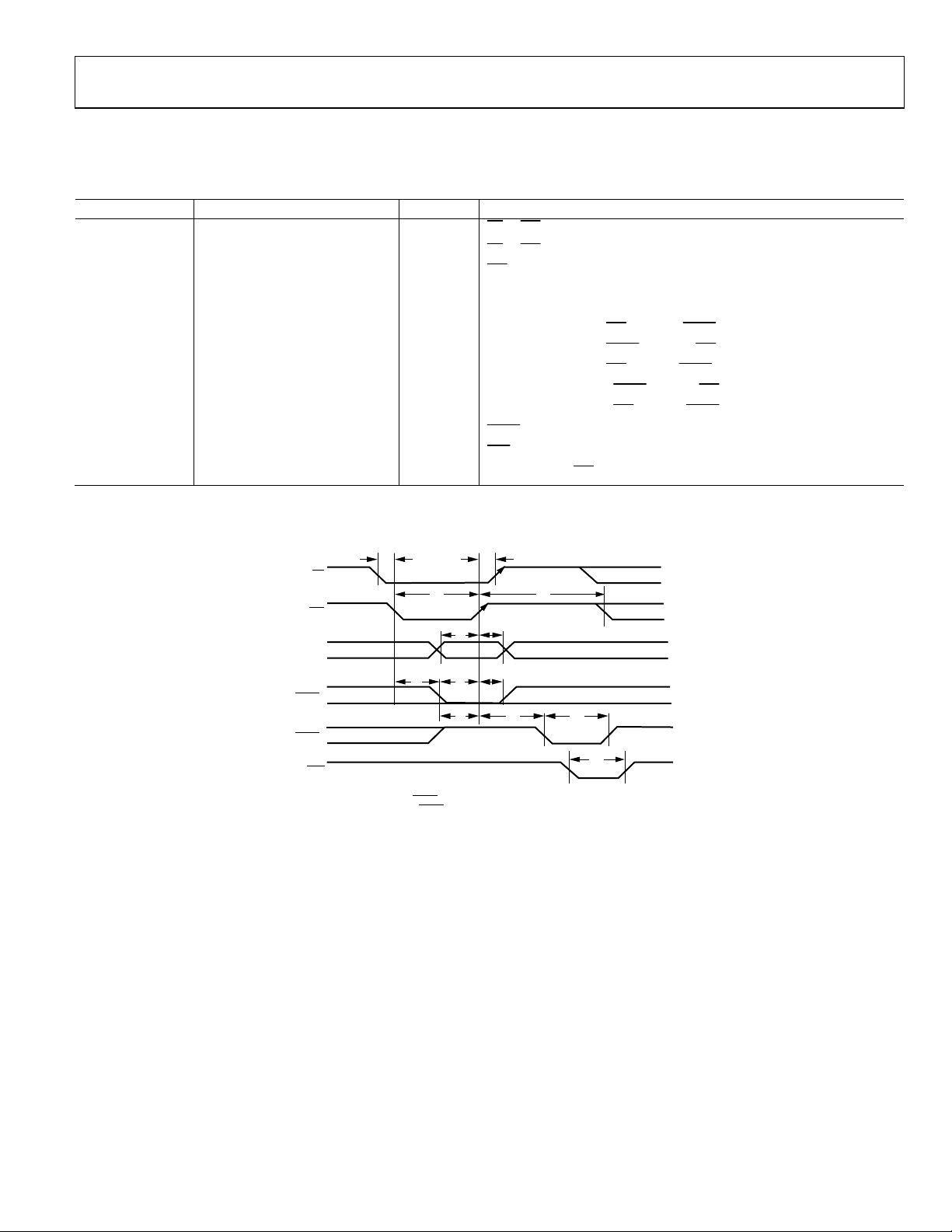
TIMING CHARACTERISTICS
1, 2, 3
V
DD
= 2.5 V to 5.5 V, all specifications T
MIN
to T
MAX
, unless otherwise noted.
Table 3.
Parameter Limit at T
MIN
, T
MAX
Unit Condition/Comments
t
1
0 ns min
CS
to WR setup time.
t
2
0 ns min
CS
to WR hold time.
t
3
20 ns min
WR
pulse width.
t
4
5 ns min Data, GAIN, BUF, HBEN setup time.
t
5
4.5 ns min Data, GAIN, BUF, HBEN hold time.
t
6
5 ns min
Synchronous mode; WR
falling to LDAC falling.
t
7
5 ns min
Synchronous mode; LDAC
falling to WR rising.
t
8
4.5 ns min
Synchronous mode; WR
rising to LDAC rising.
t
9
5 ns min
Asynchronous mode; LDAC
rising to WR rising.
t
10
4.5 ns min
Asynchronous mode; WR
rising to LDAC falling.
t
11
20 ns min
LDAC
pulse width.
t
12
20 ns min
CLR
pulse width.
t
13
50 ns min
Time between WR
cycles.
1
Guaranteed by design and characterization, not production tested.
2
All input signals are specified with t
R
= t
F
= 5 ns (10% to 90% of V
DD
) and timed from a voltage level of (V
IL
+ V
IH
)/2.
3
See Figure 2.
CS
WR
DATA,
GAIN,
BUF,
HBEN
LDAC
1
LDAC
2
CLR
NOTES:
1
SYNCHRONOUS LDAC UPDAT E MODE
2
ASYNCHRONOUS LDAC UPDAT E MODE
t
1
t
2
t
3
t
4
t
6
t
7
t
9
t
10
t
11
t
12
t
8
t
5
t
13
06852-002
Figure 2. Parallel Interface Timing Diagram
AD5330/AD5331/AD5340/AD5341
Rev. A | Page 6 of 28
ABSOLUTE MAXIMUM RATINGS
T
A
= 25°C, unless otherwise noted.
Table 4.
Parameter Rating
V
DD
to GND −0.3 V to +7 V
Digital Input Voltage to GND −0.3 V to V
DD
+ 0.3 V
Digital Output Voltage to GND −0.3 V to V
DD
+ 0.3 V
Reference Input Voltage to GND −0.3 V to V
DD
+ 0.3 V
V
OUT
to GND −0.3 V to V
DD
+ 0.3 V
Operating Temperature Range
Industrial (B Version) −40°C to +105°C
Storage Temperature Range −65°C to +150°C
Junction Temperature 150°C
TSSOP Package
Power Dissipation (T
J
max – T
A
)/θ
JA
mW
θ
JA
Thermal Impedance (20-Lead TSSOP)
1
85°C/W
θ
JA
Thermal Impedance (24-Lead TSSOP)
1
80°C/W
Reflow Soldering
Peak Temperature 260°C
Time at Peak Temperature 20 sec to 40 sec
Stresses above those listed under Absolute Maximum Ratings
may cause permanent damage to the device. This is a stress
rating only; functional operation of the device at these or any
other conditions above those indicated in the operational
section of this specification is not implied. Exposure to absolute
maximum rating conditions for extended periods may affect
device reliability.
ESD CAUTION
1
Thermal resistance (JEDEC 4-layer (2S2P) board).

AD5330/AD5331/AD5340/AD5341
Rev. A | Page 7 of 28
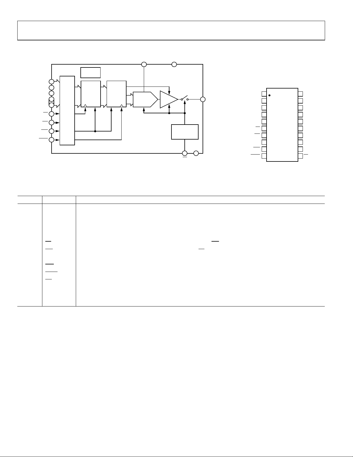
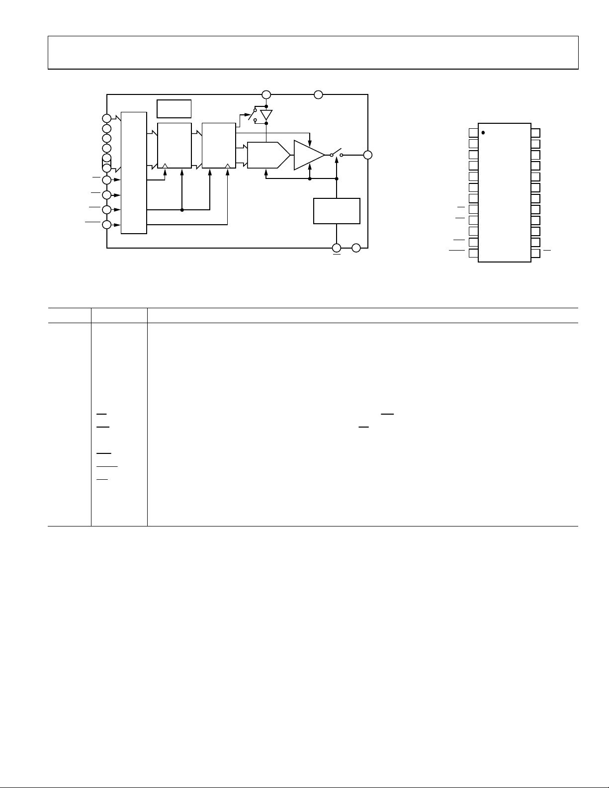
PIN CONFIGURATIONS AND FUNCTION DESCRIPTIONS
BUFFER
8-BIT
DAC
DAC
REGISTER
INPUT
REGISTER
INTERFACE LO GIC
POWER-DOW N
LOGIC
BUF
GAIN
DB
7
DB
0
.
.
CS
WR
CLR
LDAC
V
REF
V
DD
V
OUT
PD GND
AD5330
POWER-ON
RESET
RESET
10
9
7
6
13
20
8
1
3 12
4
11 5
06852-003
20
19
18
17
16
15
14
13
12
11
1
2
3
4
5
6
7
8
9
10
LDAC
GAIN
WR
CS
GND
BUF
V
REF
V
OUT
CLR
NC = NO CONNECT
NC
DB
7
DB
6
DB
5
DB
4
DB
3
DB
2
DB
1
DB
0
V
DD
PD
TOP VIEW
(Not to Scale)
AD5330
8-BIT
06852-004
Figure 3. AD5330 Functional Block Diagram Figure 4. AD5330 Pin Configuration
Table 5. AD5330 Pin Function Descriptions
Pin No. Mnemonic Description
1 BUF Buffer Control Pin. This pin controls whether the reference input to the DAC is buffered or unbuffered.
2 NC No Connect.
3 V
REF
Reference Input.
4 V
OUT
Output of DAC. Buffered output with rail-to-rail operation.
5 GND Ground reference point for all circuitry on the part.
6
CS
Active Low Chip Select Input. This is used in conjunction with WR to write data to the parallel interface.
7
WR
Active Low Write Input. This is used in conjunction with CS to write data to the parallel interface.
8 GAIN Gain Control Pin. This controls whether the output range from the DAC is 0 V to V
REF
or 0 V to 2 × V
REF
.
9
CLR
Asynchronous active low control input that clears all input registers and DAC registers to zero.
10
LDAC
Active low control input that updates the DAC registers with the contents of the input registers.
11
PD
Power-Down Pin. This active low control pin puts the DAC into power-down mode.
12 V
DD
Power Supply Input. These parts can operate from 2.5 V to 5.5 V and the supply should be decoupled with a
10 μF capacitor in parallel with a 0.1 μF capacitor to GND.
13 to 20 DB
0
to DB
7
Eight Parallel Data Inputs. DB
7
is the MSB of these eight bits.
AD5330/AD5331/AD5340/AD5341
Rev. A | Page 8 of 28
BUFFER
10-BIT
DAC
DAC
REGISTER
INPUT
REGISTER
INTERFACE LOGIC
POWER-DOW N
LOGIC
DB
8
DB
7
DB
0
.
.
CS
WR
CLR
LDAC
V
REF
V
DD
V
OUT
PD GND
AD5331
POWER-ON
RESET
RESET
10
9
7
6
13
20
1
DB
9
2
GAIN
8
3 12
4
11 5
06852-005
20
19
18
17
16
15
14
13
12
11
1
2
3
4
5
6
7
8
9
10
LDAC
GAIN
WR
CS
GND
V
REF
V
OUT
CLR
DB
7
DB
6
DB
5
DB
4
DB
3
DB
2
DB
1
DB
0
V
DD
PD
TOP VIEW
(Not to Scale)
AD5331
10-BIT
DB
8
DB
9
06852-006
Figure 5. AD5331 Functional Block Diagram Figure 6. AD5331 Pin Configuration
Table 6. AD5331 Pin Function Descriptions
Pin No. Mnemonic Description
1 DB
8
Parallel Data Input.
2 DB
9
Most Significant Bit of Parallel Data Input.
3 V
REF
Unbuffered Reference Input.
4 V
OUT
Output of DAC. Buffered output with rail-to-rail operation.
5 GND Ground reference point for all circuitry on the part.
6
CS
Active Low Chip Select Input. This is used in conjunction with WR to write data to the parallel interface.
7
WR
Active Low Write Input. This is used in conjunction with CS to write data to the parallel interface.
8 GAIN Gain Control Pin. This controls whether the output range from the DAC is 0 V to V
REF
or 0 V to 2 × V
REF
.
9
CLR
Active low control input that clears all input registers and DAC registers to zero.
10
LDAC
Active low control input that updates the DAC registers with the contents of the input registers.
11
PD
Power-Down Pin. This active low control pin puts the DAC into power-down mode.
12 V
DD
Power Supply Input. These parts can operate from 2.5 V to 5.5 V and the supply should be decoupled with a
10 μF capacitor in parallel with a 0.1 μF capacitor to GND.
13 to 20 DB
0
to DB
7
Eight Parallel Data Inputs.
AD5330/AD5331/AD5340/AD5341
Rev. A | Page 9 of 28
BUFFER
12-BIT
DAC
DAC
REGISTER
INPUT
REGISTER
POWER-DOW N
LOGIC
CS
WR
CLR
LDAC
V
REF
V
DD
V
OUT
PD GND
AD5340
POWER-ON
RESET
RESET
12
11
9
8
4 14
5
13 7
06852-007
DB
10
DB
9
DB
0
.
.
15
24
1
DB
11
2
BUF
3
GAIN
10
INTERFACE LOGIC
24
23
22
21
20
19
18
17
16
15
14
13
1
2
3
4
5
6
7
8
9
10
11
12
DB
10
PD
V
DD
DB
0
DB
1
DB
2
DB
7
DB
6
DB
3
DB
4
DB
5
12-BIT
AD5340
TOP VIEW
(Not to Scale)
DB
8
DB
9
DB
11
LDAC
GND
BUF
V
OUT
NC
V
REF
CS
WR
GAIN
CLR
06852-008
Figure 7. AD5340 Functional Block Diagram Figure 8. AD5340 Pin Configuration
Table 7. AD5340 Pin Function Descriptions
Pin No. Mnemonic Description
1 DB
10
Parallel Data Input.
2 DB
11
Most Significant Bit of Parallel Data Input.
3 BUF Buffer Control Pin. This pin controls whether the reference input to the DAC is buffered or unbuffered.
4 V
REF
Reference Input.
5 V
OUT
Output of DAC. Buffered output with rail-to-rail operation.
6 NC No Connect.
7 GND Ground reference point for all circuitry on the part.
8
CS
Active Low Chip Select Input. This is used in conjunction with WR to write data to the parallel interface.
9
WR
Active Low Write Input. This is used in conjunction with CS to write data to the parallel interface.
10 GAIN Gain Control Pin. This controls whether the output range from the DAC is 0 V to V
REF
or 0 V to 2 × V
REF
.
11
CLR
Asynchronous active low control input that clears all input registers and DAC registers to zero.
12
LDAC
Active low control input that updates the DAC registers with the contents of the input registers.
13
PD
Power-Down Pin. This active low control pin puts the DAC into power-down mode.
14 V
DD
Power Supply Input. These parts can operate from 2.5 V to 5.5 V and the supply should be decoupled with a
10 μF capacitor in parallel with a 0.1 μF capacitor to GND.
15 to 24 DB
0
to DB
9
Ten Parallel Data Inputs.
Loading...