


a |
Software Programmable |
|
Gain Amplifier |
||
|
|
|
|
|
AD526 |
|
|
|
FEATURES
Digitally Programmable Binary Gains from 1 to 16 Two-Chip Cascade Mode Achieves Binary Gain from
1 to 256 Gain Error:
0.01% Max, Gain = 1, 2, 4 (C Grade)
0.02% Max, Gain = 8, 16 (C Grade)
0.5 ppm/8C Drift Over Temperature
Fast Settling Time
10 V Signal Change:
0.01% in 4.5 ms (Gain = 16)
Gain Change:
0.01% in 5.6 ms (Gain = 16)
Low Nonlinearity: 60.005% FSR Max (J Grade)
Excellent DC Accuracy:
Offset Voltage: 0.5 mV Max (C Grade)
Offset Voltage Drift: 3 mV/8C (C Grade)
TTL-Compatible Digital Inputs
PRODUCT DESCRIPTION
The AD526 is a single-ended, monolithic software programmable gain amplifier (SPGA) that provides gains of 1, 2, 4, 8 and 16. It is complete, including amplifier, resistor network and TTL-compatible latched inputs, and requires no external components.
Low gain error and low nonlinearity make the AD526 ideal for precision instrumentation applications requiring programmable gain. The small signal bandwidth is 350 kHz at a gain of 16. In addition, the AD526 provides excellent dc precision. The FETinput stage results in a low bias current of 50 pA. A guaranteed maximum input offset voltage of 0.5 mV max (C grade) and low gain error (0.01%, G = 1, 2, 4, C grade) are accomplished using Analog Devices’ laser trimming technology.
To provide flexibility to the system designer, the AD526 can be operated in either latched or transparent mode. The force/sense configuration preserves accuracy when the output is connected to remote or low impedance loads.
The AD526 is offered in one commercial (0°C to +70°C) grade, J, and three industrial grades, A, B and C, which are specified from –40°C to +85°C. The S grade is specified from –55°C to +125°C. The military version is available processed to MILSTD 883B, Rev C. The J grade is supplied in a 16-lead plastic DIP, and the other grades are offered in a 16-lead hermetic side-brazed ceramic DIP.
REV. D
Information furnished by Analog Devices is believed to be accurate and reliable. However, no responsibility is assumed by Analog Devices for its use, nor for any infringements of patents or other rights of third parties which may result from its use. No license is granted by implication or otherwise under any patent or patent rights of Analog Devices.
PIN CONFIGURATION
DIG GND |
|
|
|
|
|
A1 |
|
1 |
|
|
|
16 |
|||
NULL |
|
|
|
|
|
A0 |
|
2 |
|
|
|
15 |
|||
VIN |
|
|
|
|
|
CS |
|
3 |
|
|
|
14 |
|||
NULL |
|
AD526 |
|
CLK |
|||
4 |
13 |
||||||
ANALOG GND 2 |
|
TOP VIEW |
|
A2 |
|||
5 |
(Not to Scale) |
12 |
|||||
ANALOG GND 1 |
|
|
|
|
|
B |
|
6 |
|
|
|
11 |
|
||
–V |
|
|
|
|
|
+V |
|
7 |
|
|
|
10 |
S |
||
S |
|
|
|
|
|
|
|
VOUT SENSE |
|
|
|
|
|
VOUT FORCE |
|
8 |
|
|
|
9 |
|||
|
|
|
|
|
|
|
|
APPLICATION HIGHLIGHTS
1.Dynamic Range Extension for ADC Systems: A single AD526 in conjunction with a 12-bit ADC can provide
96 dB of dynamic range for ADC systems.
2.Gain Ranging Preamps: The AD526 offers complete digital gain control with precise gains in binary steps from 1 to 16. Additional gains of 32, 64, 128 and 256 are possible by cascading two AD526s.
ORDERING GUIDE
|
Temperature |
Package |
Package |
Model |
Range |
Descriptions |
Options |
|
|
|
|
AD526JN |
Commercial |
16-Lead Plastic DIP |
N-16 |
AD526AD |
Industrial |
16-Lead Cerdip |
D-16 |
AD526BD |
Industrial |
16-Lead Cerdip |
D-16 |
AD526CD |
Industrial |
16-Lead Cerdip |
D-16 |
AD526SD |
Military |
16-Lead Cerdip |
D-16 |
AD526SD/883B |
Military |
16-Lead Cerdip |
D-16 |
5962-9089401MEA* |
Military |
16-Lead Cerdip |
D-16 |
|
|
|
|
*Refer to official DESC drawing for tested specifications.
One Technology Way, P.O. Box 9106, Norwood, MA 02062-9106, U.S.A.
Tel: 781/329-4700 |
World Wide Web Site: http://www.analog.com |
Fax: 781/326-8703 |
© Analog Devices, Inc., 1999 |
AD526–SPECIFICATIONS (@ VS = 615 V, RL = 2 kV and TA = +258C unless otherwise noted)
|
|
AD526J |
|
|
AD526A |
|
|
AD526B/S |
|
|
AD526C |
|
|
Model |
Min |
Typ |
Max |
Min |
Typ |
Max |
Min |
Typ |
Max |
Min |
Typ |
Max |
Units |
|
|
|
|
|
|
|
|
|
|
|
|
|
|
GAIN |
|
|
|
|
|
|
|
|
|
|
|
|
|
Gain Range |
|
|
|
|
|
|
|
|
|
|
|
|
|
(Digitally Programmable) |
1, 2, 4, 8, 16 |
|
|
1, 2, 4, 8, 16 |
|
1, 2, 4, 8, 16 |
|
1, 2, 4, 8, 16 |
|
||||
Gain Error |
|
|
|
|
|
|
|
|
|
|
|
|
|
Gain = 1 |
|
|
0.05 |
|
|
0.02 |
|
|
0.01 |
|
|
0.01 |
% |
Gain = 2 |
|
|
0.05 |
|
|
0.03 |
|
|
0.02 |
|
|
0.01 |
% |
Gain = 4 |
|
|
0.10 |
|
|
0.03 |
|
|
0.02 |
|
|
0.01 |
% |
Gain = 8 |
|
|
0.15 |
|
|
0.07 |
|
|
0.04 |
|
|
0.02 |
% |
Gain = 16 |
|
|
0.15 |
|
|
0.07 |
|
|
0.04 |
|
|
0.02 |
% |
Gain Error Drift |
|
|
|
|
|
|
|
|
|
|
|
|
|
Over Temperature |
|
|
|
|
|
|
|
|
|
|
|
|
ppm/°C |
G = 1 |
|
0.5 |
2.0 |
|
0.5 |
2.0 |
|
0.5 |
2.0 |
|
0.5 |
2.0 |
|
G = 2 |
|
0.5 |
2.0 |
|
0.5 |
2.0 |
|
0.5 |
2.0 |
|
0.5 |
2.0 |
ppm/°C |
G = 4 |
|
0.5 |
3.0 |
|
0.5 |
3.0 |
|
0.5 |
3.0 |
|
0.5 |
3.0 |
ppm/°C |
G = 8 |
|
0.5 |
5.0 |
|
0.5 |
5.0 |
|
0.5 |
5.0 |
|
0.5 |
5.0 |
ppm/°C |
G = 16 |
|
1.0 |
5.0 |
|
1.0 |
5.0 |
|
1.0 |
5.0 |
|
1.0 |
5.0 |
ppm/°C |
Gain Error (TMIN to TMAX) |
|
|
|
|
|
0.03 |
|
|
0.02 |
|
|
0.015 |
|
Gain = 1 |
|
|
0.06 |
|
|
|
|
|
|
% |
|||
Gain = 2 |
|
|
0.06 |
|
|
0.04 |
|
|
0.03 |
|
|
0.015 |
% |
Gain = 4 |
|
|
0.12 |
|
|
0.04 |
|
|
0.03 |
|
|
0.015 |
% |
Gain = 8 |
|
|
0.17 |
|
|
0.08 |
|
|
0.05 |
|
|
0.03 |
% |
Gain = 16 |
|
|
0.17 |
|
|
0.08 |
|
|
0.05 |
|
|
0.03 |
% |
Nonlinearity |
|
|
|
|
|
|
|
|
|
|
|
|
|
Gain = 1 |
|
|
0.005 |
|
|
0.005 |
|
|
0.005 |
|
|
0.0035 |
% FSR |
Gain = 2 |
|
|
0.001 |
|
|
0.001 |
|
|
0.001 |
|
|
0.001 |
% FSR |
Gain = 4 |
|
|
0.001 |
|
|
0.001 |
|
|
0.001 |
|
|
0.001 |
% FSR |
Gain = 8 |
|
|
0.001 |
|
|
0.001 |
|
|
0.001 |
|
|
0.001 |
% FSR |
Gain = 16 |
|
|
0.001 |
|
|
0.001 |
|
|
0.001 |
|
|
0.001 |
% FSR |
Nonlinearity (TMIN to TMAX) |
|
|
|
|
|
0.01 |
|
|
0.01 |
|
|
0.007 |
|
Gain = 1 |
|
|
0.01 |
|
|
|
|
|
|
% FSR |
|||
Gain = 2 |
|
|
0.001 |
|
|
0.001 |
|
|
0.001 |
|
|
0.001 |
% FSR |
Gain = 4 |
|
|
0.001 |
|
|
0.001 |
|
|
0.001 |
|
|
0.001 |
% FSR |
Gain = 8 |
|
|
0.001 |
|
|
0.001 |
|
|
0.001 |
|
|
0.001 |
% FSR |
Gain = 16 |
|
|
0.001 |
|
|
0.001 |
|
|
0.001 |
|
|
0.001 |
% FSR |
VOLTAGE OFFSET, ALL GAINS |
|
|
|
|
|
|
|
|
|
|
|
|
|
Input Offset Voltage |
|
0.4 |
1.5 |
|
0.25 |
0.7 |
|
0.25 |
0.5 |
|
0.25 |
0.5 |
mV |
Input Offset Voltage Drift Over |
|
|
|
|
|
|
|
|
|
|
|
|
µV/°C |
Temperature |
|
5 |
20 |
|
3 |
10 |
|
3 |
10 |
|
3 |
10 |
|
Input Offset Voltage |
|
|
|
|
|
|
|
|
|
|
|
|
|
TMIN to TMAX |
|
|
2.0 |
|
|
1.0 |
|
|
0.8 |
|
|
0.8 |
mV |
Input Offset Voltage vs. Supply |
|
|
|
|
|
|
|
|
|
|
|
|
|
(VS ± 10%) |
80 |
|
|
80 |
|
|
84 |
|
|
90 |
|
|
dB |
INPUT BIAS CURRENT |
|
|
|
|
|
|
|
|
|
|
|
|
|
Over Input Voltage Range ± 10 V |
|
50 |
150 |
|
50 |
150 |
|
50 |
150 |
|
50 |
150 |
pA |
|
|
|
|
|
|
|
|
|
|
|
|
|
|
ANALOG INPUT |
|
|
|
|
|
|
|
|
|
|
|
|
|
CHARACTERISTICS |
|
|
|
|
|
|
|
|
|
|
|
|
|
Voltage Range |
|
±12 |
|
|
±12 |
|
|
±12 |
|
|
±12 |
|
|
(Linear Operation) |
610 |
|
610 |
|
610 |
|
610 |
|
V |
||||
Capacitance |
|
5 |
|
|
5 |
|
|
5 |
|
|
5 |
|
pF |
|
|
|
|
|
|
|
|
|
|
|
|
|
|
RATED OUTPUT |
|
±12 |
|
|
±12 |
|
|
±12 |
|
|
±12 |
|
|
Voltage |
610 |
|
610 |
|
610 |
|
610 |
|
V |
||||
Current (VOUT = ±10 V) |
|
±10 |
|
65 |
±10 |
|
65 |
±10 |
|
65 |
±10 |
|
mA |
Short-Circuit Current |
15 |
30 |
|
15 |
30 |
|
15 |
30 |
|
15 |
30 |
|
mA |
DC Output Resistance |
|
0.002 |
|
|
0.002 |
|
|
0.002 |
|
|
0.002 |
|
Ω |
Load Capacitance |
|
|
|
|
|
|
|
|
|
|
|
|
|
(For Stable Operation) |
|
700 |
|
|
700 |
|
|
700 |
|
|
700 |
|
pF |
|
|
|
|
|
|
|
|
|
|
|
|
|
|
–2– |
REV. D |
|
|
|
|
|
|
|
|
|
|
|
|
|
AD526 |
|
|
|
AD526J |
|
|
AD526A |
|
|
AD526B/S |
|
|
AD526C |
|
|
Model |
Min |
Typ |
Max |
Min |
Typ |
Max |
Min |
Typ |
Max |
Min |
Typ |
Max |
Units |
|
|
|
|
|
|
|
|
|
|
|
|
|
|
NOISE, ALL GAINS |
|
|
|
|
|
|
|
|
|
|
|
|
|
Voltage Noise, RTI |
|
|
|
|
|
|
|
|
|
|
|
|
µV p-p |
0.1 Hz to 10 Hz |
|
3 |
|
|
3 |
|
|
3 |
|
|
3 |
|
|
Voltage Noise Density, RTI |
|
|
|
|
|
|
|
|
|
|
|
|
nV√Hz |
f = 10 Hz |
|
70 |
|
|
70 |
|
|
70 |
|
|
70 |
|
|
f = 100 Hz |
|
60 |
|
|
60 |
|
|
60 |
|
|
60 |
|
nV√Hz |
f = 1 kHz |
|
30 |
|
|
30 |
|
|
30 |
|
|
30 |
|
nV√Hz |
f = 10 kHz |
|
25 |
|
|
25 |
|
|
25 |
|
|
35 |
|
nV√Hz |
DYNAMIC RESPONSE |
|
|
|
|
|
|
|
|
|
|
|
|
|
–3 dB Bandwidth (Small Signal) |
|
|
|
|
|
|
|
|
|
|
|
|
|
G = 1 |
|
4.0 |
|
|
4.0 |
|
|
4.0 |
|
|
4.0 |
|
MHz |
G = 2 |
|
2.0 |
|
|
2.0 |
|
|
2.0 |
|
|
2.0 |
|
MHz |
G = 4 |
|
1.5 |
|
|
1.5 |
|
|
1.5 |
|
|
1.5 |
|
MHz |
G = 8 |
|
0.65 |
|
|
0.65 |
|
|
0.65 |
|
|
0.65 |
|
MHz |
G = 16 |
|
0.35 |
|
|
0.35 |
|
|
0.35 |
|
|
0.35 |
|
MHz |
Signal Settling Time to 0.01% |
|
|
|
|
|
|
|
|
|
|
|
|
|
( VOUT = ± 10 V) |
|
|
|
|
|
|
|
|
|
|
|
|
µs |
G = 1 |
|
2.1 |
4 |
|
2.1 |
4 |
|
2.1 |
4 |
|
2.1 |
4 |
|
G = 2 |
|
2.5 |
5 |
|
2.5 |
5 |
|
2.5 |
5 |
|
2.5 |
5 |
µs |
G = 4 |
|
2.7 |
5 |
|
2.7 |
5 |
|
2.7 |
5 |
|
2.7 |
5 |
µs |
G = 8 |
|
3.6 |
7 |
|
3.6 |
7 |
|
3.6 |
7 |
|
3.6 |
7 |
µs |
G = 16 |
|
4.1 |
7 |
|
4.1 |
7 |
|
4.1 |
7 |
|
4.1 |
7 |
µs |
Full Power Bandwidth |
|
|
|
|
|
|
|
|
|
|
|
|
|
G = 1, 2, 4 |
|
0.10 |
|
|
0.10 |
|
|
0.10 |
|
|
0.10 |
|
MHz |
G = 8, 16 |
|
0.35 |
|
|
0.35 |
|
|
0.35 |
|
|
0.35 |
|
MHz |
Slew Rate |
|
|
|
|
|
|
|
|
|
|
|
|
V/µs |
G = 1, 2, 4 |
4 |
6 |
|
4 |
6 |
|
4 |
6 |
|
4 |
6 |
|
|
G = 8, 16 |
18 |
24 |
|
18 |
24 |
|
18 |
24 |
|
18 |
24 |
|
V/µs |
DIGITAL INPUTS |
|
|
|
|
|
|
|
|
|
|
|
|
|
(TMIN to TMAX) |
|
|
|
|
|
|
|
|
|
|
|
|
µA |
Input Current (VH = 5 V) |
60 |
100 |
140 |
60 |
100 |
140 |
60 |
100 |
140 |
60 |
100 |
140 |
|
Logic “1” |
2 |
|
6 |
2 |
|
6 |
2 |
|
6 |
2 |
|
6 |
V |
Logic “0” |
0 |
|
0.8 |
0 |
|
0.8 |
0 |
|
0.8 |
0 |
|
0.8 |
V |
TIMING1 |
|
|
|
|
|
|
|
|
|
|
|
|
|
(VL = 0.2 V, VH = 3.7 V) |
|
|
|
|
|
|
|
|
|
|
|
|
|
A0, A1, A2 |
|
|
|
|
|
|
|
|
|
|
|
|
|
TC |
50 |
|
|
50 |
|
|
50 |
|
|
50 |
|
|
ns |
TS |
30 |
|
|
30 |
|
|
30 |
|
|
30 |
|
|
ns |
TH |
30 |
|
|
30 |
|
|
30 |
|
|
30 |
|
|
ns |
B |
|
|
|
|
|
|
|
|
|
|
|
|
|
TC |
50 |
|
|
50 |
|
|
50 |
|
|
50 |
|
|
ns |
TS |
40 |
|
|
40 |
|
|
40 |
|
|
40 |
|
|
ns |
TH |
10 |
|
|
10 |
|
|
10 |
|
|
30 |
|
|
ns |
TEMPERATURE RANGE |
|
|
|
|
|
|
|
|
|
|
|
|
°C |
Specified Performance |
0 |
|
+70 |
–40 |
|
+85 |
–40/–55 |
+85/+125 |
–40 |
|
+85 |
||
Storage |
–65 |
|
+125 |
–65 |
|
+150 |
–65 |
|
+150 |
–65 |
|
+150 |
°C |
POWER SUPPLY |
|
|
|
|
|
|
|
|
|
|
|
|
|
Operating Range |
64.5 |
|
616.5 |
64.5 |
|
616.5 |
64.5 |
|
616.5 |
64.5 |
|
616.5 |
V |
Positive Supply Current |
|
10 |
14 |
|
10 |
14 |
|
10 |
14 |
|
10 |
14 |
mA |
Negative Supply Current |
|
10 |
13 |
|
10 |
13 |
|
10 |
13 |
|
10 |
13 |
mA |
PACKAGE OPTIONS |
|
|
|
|
|
|
|
|
|
|
|
|
|
Plastic (N-16) |
AD526JN |
|
|
|
|
|
|
|
|
|
|
|
|
Ceramic DIP (D-16) |
|
|
|
AD526AD |
|
AD526BD AD526SD |
|
AD526CD |
|
||||
|
|
|
|
|
|
|
|
AD526SD/883B |
|
|
|
|
|
NOTES |
|
|
|
|
|
|
|
|
|
|
|
|
|
1Refer to Figure 25 for definitions. FSR = Full Scale Range = 20 V. RTI = Referred to Input.
Specifications subject to change without notice.
Specifications shown in boldface are tested on all production units at final electrical test. All min and max specifications are guaranteed, although only those shown in boldface are tested on all production units.
REV. D |
–3– |
|
AD526–Typical Performance Characteristics
|
20 |
|
|
|
|
|
30 |
|
|
–6V |
15 |
|
|
|
|
–6V |
|
|
|
SWING |
|
+258C |
|
|
SWING |
|
@ VS = 615V |
|
|
|
|
|
|
20 |
|
||||
|
|
|
RL = 2kV |
|
|
|
|
|
|
VOLTAGE |
|
|
|
|
VOLTAGE |
|
|
|
|
10 |
|
|
|
|
|
|
|
||
OUTPUT |
|
|
|
|
|
OUTPUT |
10 |
|
|
5 |
|
|
|
|
|
|
|
||
|
|
|
|
|
|
|
|
|
|
|
0 |
|
|
|
|
|
0 |
|
|
|
0 |
5 |
10 |
15 |
20 |
|
100 |
1k |
10k |
|
|
SUPPLY VOLTAGE –6V |
|
|
|
LOAD RESISTANCE –V |
|
||
|
|
|
|
|
|
|
|
|
|
Figure 1. Output Voltage Swing vs. |
Figure 2. Output Voltage Swing vs. |
Supply Voltage, G = 16 |
|
|
Load Resistance |
|
|
|
|||||
|
100nA |
|
|
|
|
|
75 |
|
|
|
|
BIASINPUTCURRENT |
10nA |
|
|
|
|
|
pA |
|
|
VS = 615V |
|
|
|
|
|
|
|
BIASINPUTCURRENT – |
|
|
|
|
|
|
|
|
|
|
|
|
50 |
|
|
|
|
|
1nA |
|
|
|
|
|
|
|
|
|
|
|
100pA |
|
|
|
|
|
|
|
|
|
|
|
|
|
|
|
|
|
25 |
|
|
|
|
|
10pA |
|
|
|
|
|
|
|
|
|
|
|
1pA |
–20 |
20 |
60 |
100 |
140 |
0 |
–5 |
0 |
5 |
10 |
|
–60 |
–10 |
|||||||||
|
|
TEMPERATURE –8C |
|
|
|
INPUT VOLTAGE – V |
|
||||
Figure 4. Input Bias Current vs.
Temperature |
|
|
|||
|
25 |
|
|
|
|
p-p |
|
|
|
|
|
V |
20 |
|
|
GAIN = 8, 16 |
|
– |
|
|
|||
|
|
|
|
|
|
RESPONSE |
15 |
GAIN = 1, 2, 4 |
|
|
|
|
|
|
|||
|
|
|
|
|
|
POWER |
10 |
|
|
|
|
|
|
|
|
|
|
FULL |
5 |
|
|
|
|
|
|
|
|
|
|
|
0 |
10k |
100k |
1M |
10M |
|
1k |
||||
|
|
|
FREQUENCY – Hz |
|
|
Figure 5. Input Bias Current vs. Input
Voltage |
|
|
|
|
|
|
|
|
100 |
|
|
|
615V WITH 1V p-p |
||
|
|
|
|
|
|||
dB |
|
|
|
|
SINE WAVE |
|
|
80 |
|
|
|
|
|
|
|
– |
|
|
|
|
|
|
|
|
|
|
|
|
|
|
|
REJECTION |
|
|
|
|
|
+SUPPLY |
|
60 |
|
|
|
|
|
|
|
|
|
|
|
|
|
|
|
SUPPLY |
40 |
|
|
|
|
|
|
|
|
|
–SUPPLY |
|
|
||
POWER |
20 |
|
|
|
|
|
|
|
|
|
|
|
|
|
|
|
10 |
10 |
100 |
1k |
10k |
100k |
1M |
|
1 |
||||||
FREQUENCY – Hz
Figure 7. Large Signal Frequency |
Figure 8. PSRR vs. Frequency |
Response |
|
|
20 |
|
|
|
|
– pA |
15 |
|
|
|
|
CURRENT |
10 |
|
VIN = 0 |
|
|
BIAS |
|
|
|
|
|
INPUT |
5 |
|
|
|
|
|
|
|
|
|
|
|
0 |
5 |
10 |
15 |
20 |
|
0 |
SUPPLY VOLTAGE –6V
Figure 3. Input Bias Current vs. Supply Voltage
|
20 |
|
|
|
|
16 |
|
|
|
|
|
|
|
|
|
|
10 |
|
|
|
|
|
|
|
|
|
|
|
|
|
8 |
|
|
|
|
|
|
4 |
|
GAIN |
|
|
|
|
|
2 |
|
1 |
|
|
|
|
|
|
|
|
|
|
|
|
|
|
|
|
|
|
|
|
|
|
1 |
|
10 |
100 |
1k |
10k |
100k |
1M |
10M |
|
|
|
FREQUENCY – Hz |
|
|
||
Figure 6. Gain vs. Frequency
|
1.0002 |
|
|
|
|
|
|
|
|
|
|
|
GAIN |
1.0001 |
|
|
|
|
|
|
|
|
|
|
|
|
|
|
|
|
|
|
|
|
|
|
||
|
|
|
|
|
|
|
|
|
|
|
|
|
NORMALIZED |
1.0000 |
|
|
|
|
|
|
|
|
|
|
|
|
|
|
|
|
|
|
|
|
|
|
|
|
|
0.9999 |
|
|
|
|
|
|
|
|
|
|
|
|
|
|
|
|
|
|
|
|
|
|
|
|
|
0.9998 |
|
|
|
|
|
|
|
|
|
|
|
|
|
–20 |
20 |
60 |
100 |
140 |
||||||
|
–60 |
|||||||||||
TEMPERATURE –8C
Figure 9. Normalized Gain vs. Temperature, Gain = 1
–4– |
REV. D |

AD526
1000 |
|
|
|
|
|
0.006 |
|
|
|
|
|
Hz |
|
|
|
|
|
0.004 |
|
|
|
|
|
VOLTAGENOISEINPUT– nV/ |
|
|
|
|
NONLINEARITY– %FSR |
|
|
|
|
|
|
|
|
|
|
0.002 |
|
|
|
|
|
||
|
|
|
|
|
|
|
|
|
|
|
|
100 |
|
|
|
|
|
|
|
|
|
|
|
|
|
|
|
|
|
0.000 |
|
|
|
|
|
|
|
|
|
|
|
–0.002 |
|
|
|
|
|
10 |
|
|
|
|
|
–0.004 |
–20 |
20 |
60 |
100 |
140 |
10 |
100 |
1k |
10k |
100k |
|
–60 |
FREQUENCY – Hz |
TEMPERATURE –8C |
|
|
Figure 10. Noise Spectral Density |
Figure 11. Nonlinearity vs. |
|
Temperature, Gain = 1 |
Figure 12. Wideband Output Noise, G = 16 (Amplified by 10)
Figure 13. Large Signal Pulse
Response and Settling Time,*
G = 1
Figure 16. Small Signal Pulse
Response, G = 2
Figure 14. Small Signal Pulse
Response, G = 1
Figure 17. Large Signal Pulse
Response and Settling Time,*
G = 4
Figure 15. Large Signal Pulse
Response and Settling Time,*
G = 2
Figure 18. Small Signal Pulse
Response, G = 4
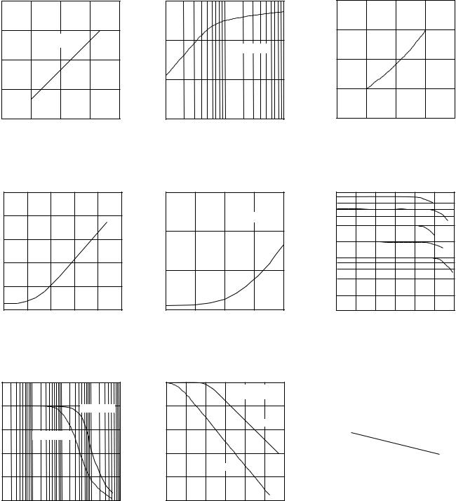
*For Settling Time Traces, 0.01% = 1/2 Vertical Division
REV. D |
–5– |
 Loading...