


AD626AR-REEL7
Table of contents
 Loading...
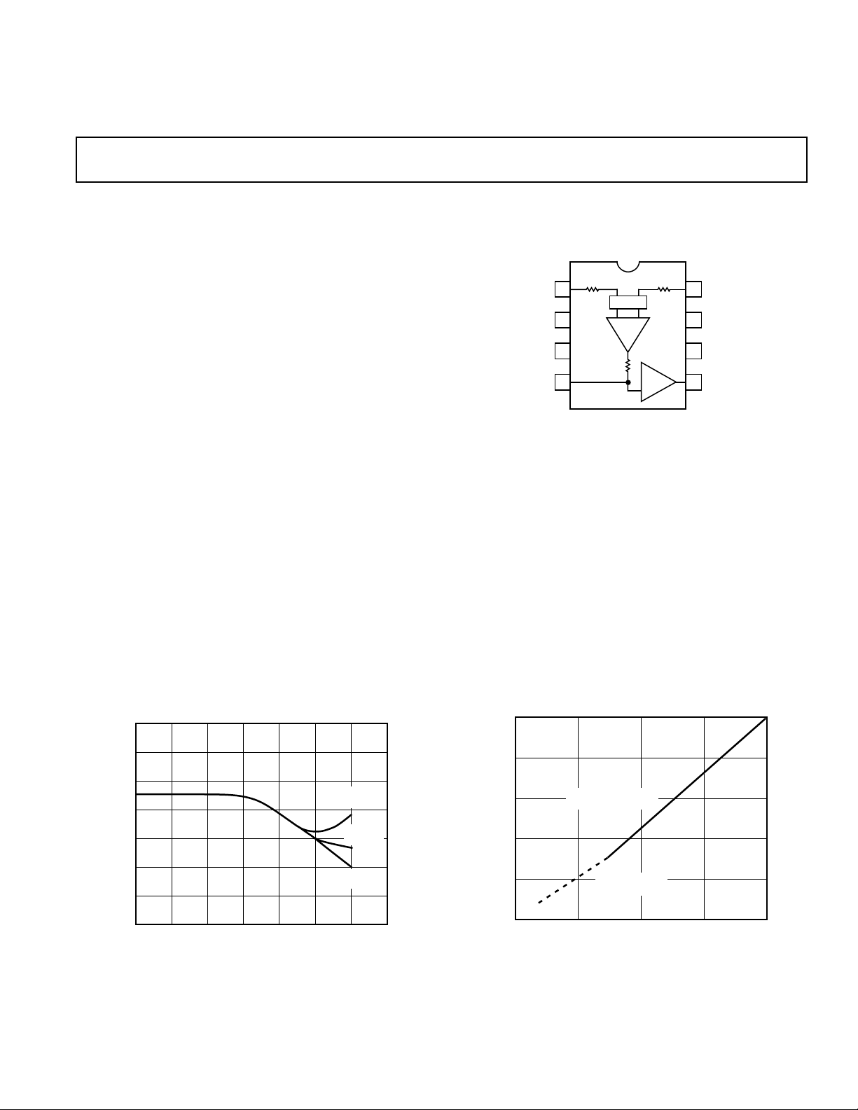
1
2
3
4
8
7
6
5
AD626
1/6
200kV
–IN
ANALOG
GND
–V
S
FILTER
+IN
G = 100
OUT
+V
S
100kV
G
=
2
G = 30
200kV
Low Cost, Single Supply
25
0
5
15
5
2
10
1
20
4
3
POWER SUPPLY VOLTAGE – 6Volts
INPUT COMMON MODE RANGE – Volts
6VCM FOR SINGLE
AND DUAL SUPPLIES
6VCM FOR DUAL
SUPPLIES ONLY
a
FEATURES
Pin Selectable Gains of 10 and 100
True Single Supply Operation
Single Supply Range of +2.4 V to +10 V
Dual Supply Range of ⴞ1.2 V to ⴞ6 V
Wide Output Voltage Range of 30 mV to 4.7 V
Optional Low-Pass Filtering
Excellent DC Performance
Low Input Offset Voltage: 500 V max
Large Common-Mode Range: 0 V to +54 V
Low Power: 1.2 mW (V
Good CMR of 90 dB typ
AC Performance
Fast Settling Time: 24 s (0.01%)
Includes Input Protection
Series Resistive Inputs (R
RFI Filters Included
Allows 50 V Continuous Overload
APPLICATIONS
Current Sensing
Interface for Pressure Transducers, Position Indicators,
Strain Gages, and Other Low Level Signal Sources
PRODUCT DESCRIPTION
The AD626 is a low cost, true single supply differential amplifier designed for amplifying and low-pass filtering small differential voltages from sources having a large common-mode voltage.
The AD626 can operate from either a single supply of +2.4 V to
+10 V, or dual supplies of ±1.2 V to ±6 V. The input common-
mode range of this amplifier is equal to 6 (+V
provides a +24 V CMR while operating from a +5 V supply.
Furthermore, the AD626 features a CMR of 90 dB typ.
= +5 V)
S
= 200 k⍀)
IN
– 1 V) which
S
Differential Amplifier
AD626
CONNECTION DIAGRAM
8-Lead Plastic Mini-DIP (N)
and SOIC (SO) Packages
The amplifier’s inputs are protected against continuous overload
of up to 50 V, and RFI filters are included in the attenuator
network. The output range is +0.03 V to +4.9 V using a +5 V
supply. The amplifier provides a preset gain of 10, but gains between 10 to 100 can be easily configured with an external resistor. Furthermore, a gain of 100 is available by connecting the G
= 100 pin to analog ground. The AD626 also offers low-pass
filter capability by connecting a capacitor between the filter pin
and analog ground.
The AD626A and AD626B operate over the industrial tempera-
ture range of –40°C to +85°C. The AD626 is available in two
8-lead packages: a plastic mini-DIP and SOIC.
160
140
100
80
60
CMRR – dB
REV. C
Information furnished by Analog Devices is believed to be accurate and
reliable. However, no responsibility is assumed by Analog Devices for its
use, nor for any infringements of patents or other rights of third parties
which may result from its use. No license is granted by implication or
otherwise under any patent or patent rights of Analog Devices.
40
20
0
0.1
Common-Mode Rejection vs. Frequency
G = 10,100
V
= +5V
S
G = 100
V
= 65V
S
G = 10
V
= 65V
S
1
FREQUENCY – Hz
1M
100k10k1k10010
Input Common-Mode Range vs. Supply
One Technology Way, P.O. Box 9106, Norwood, MA 02062-9106, U.S.A.
Tel: 781/329-4700 World Wide Web Site: http://www.analog.com
Fax: 781/326-8703 © Analog Devices, Inc., 1999

AD626–SPECIFICATIONS
SINGLE SUPPLY
Model AD626A AD626B
Parameter Condition Min Typ Max Min Typ Max Units
GAIN
Gain Accuracy Total Error
Gain = 10 @ V
Gain = 100 @ V
Over Temperature, T
Gain Linearity
Gain = 10 @ V
Gain = 100 @ V
OFFSET VOLTAGE
Input Offset Voltage 1.9 2.5 1.9 2.5 mV
vs. Temperature T
vs. Temperature T
vs. Supply Voltage (PSR)
+PSR 74 80 74 80 dB
–PSR 64 66 64 66 dB
COMMON-MODE REJECTION R
+CMR Gain = 10, 100 f = 100 Hz, V
±CMR Gain = 10, 100 f = 10 kHz, V
–CMR Gain = 10, 100
COMMON-MODE VOLTAGE RANGE
+CMV Gain = 10 CMR > 85 dB +24 +24 V
–CMV Gain = 10 CMR > 85 dB –2 –2 V
INPUT
Input Resistance
Differential 200 200 kΩ
Common Mode 100 100 kΩ
Input Voltage Range (Common Mode) 6 (VS – l) 6 (VS – l) V
OUTPUT
Output Voltage Swing R
Positive Gain = 10 4.7 4.90 4.7 4.90 V
Negative Gain = 10 0.03 0.03 V
Short Circuit Current
+I
SC
NOISE
Voltage Noise RTI
Gain = 10 f = 0.1 Hz–10 Hz 2 2 µV p-p
Gain = 100 f = 0.1 Hz–10 Hz 2 2 µV p-p
Gain = 10 f = 1 kHz 0.25 0.25 µV/√Hz
Gain = 100 f = 1 kHz 0.25 0.25 µV/√Hz
DYNAMIC RESPONSE
–3 dB Bandwidth V
Slew Rate, T
Settling Time to 0.01%, 1 V Step 24 22 µs
POWER SUPPLY
Operating Range T
Quiescent Current Gain = 10 0.16 0.20 0.16 0.20 mA
TRANSISTOR COUNT # of Transistors
NOTES
1
At temperatures above +25°C, –CMV degrades at the rate of 12 mV/ °C; i.e., @ +25°C CMV = –2 V, @ +85°C CMV = –1.28 V.
Specifications subject to change without notice.
MIN
(@ +VS = +5 V and TA = +25ⴗC)
= T
A
MIN–TMAX
1
to T
MAX
≥ 100 mV dc 0.4 1.0 0.2 0.6 %
OUT
≥ 100 mV dc 0.1 1.0 0.5 0.6 %
OUT
G = 10 50 30 ppm/°C
G = 100 150 120 ppm/°C
≥ 100 mV dc 0.014 0.016 0.014 0.016 %
OUT
≥ 100 mV dc 0.014 0.02 0.014 0.02 %
OUT
MIN–TMAX
MIN–TMAX
= 10 kΩ
L
, G = 10 or 100 2.9 2.9 mV
, G = 10 or 100 6 6 µV/°C
= +24 V 66 90 80 90 dB
CM
= 6 V 55 64 55 64 dB
CM
f = 100 Hz, VCM = –2 V 60 85 73 85 dB
= 10 kΩ
L
Gain = 100 4.7 4.90 4.7 4.90 V
Gain = 100 0.03 0.03 V
12 12 mA
= +1 V dc 100 100 kHz
OUT
Gain = 10 0.17 0.22 0.17 0.22 V/µs
Gain = 100 0.1 0.17 0.1 0.17 V/µs
= T
A
MIN–TMAX
2.4 5 12 2.4 5 10 V
Gain = 100 0.23 0.29 0.23 0.29 mA
46 46
–2–
REV. C
DUAL SUPPLY
Model AD626A AD626B
Parameter Condition Min Typ Max Min Typ Max Units
GAIN
Gain Accuracy Total Error
Gain = 10 R
Gain = 100 0.25 1.0 0.15 0.6 %
Over Temperature, T
Gain Linearity
Gain = 10 0.045 0.055 0.045 0.055 %
Gain = 100 0.01 0.015 0.01 0.015 %
OFFSET VOLTAGE
Input Offset Voltage 50 500 50 250 µV
vs. Temperature T
vs. Temperature T
vs. Supply Voltage (PSR)
+PSR 74 80 74 80 dB
–PSR 64 66 64 66 dB
COMMON-MODE REJECTION R
±CMR Gain = 10, 100 f = 100 Hz, V
±CMR Gain = 10, 100 f = 10 kHz, V
COMMON-MODE VOLTAGE RANGE
+CMV Gain = 10 CMR > 85 dB 26.5 26.5 V
–CMV Gain = 10 CMR > 85 dB 32.5 32.5 V
INPUT
Input Resistance
Differential 200 200 kΩ
Common Mode 110 110 kΩ
Input Voltage Range (Common Mode) 6 (VS – 1) 6 (VS – 1) V
OUTPUT
Output Voltage Swing R
Positive Gain = 10, 100 4.7 4.90 4.7 4.90 V
Negative Gain = 10 1.65 2.1 1.65 2.1 V
Short Circuit Current
+I
SC
–I
SC
NOISE
Voltage Noise RTI
Gain = 10 f = 0.1 Hz–10 Hz 2 2 µV p-p
Gain = 100 f = 0.1 Hz–10 Hz 2 2 µV p-p
Gain = 10 f = 1 kHz 0.25 0.25 µV/√Hz
Gain = 100 f = 1 kHz 0.25 0.25 µV/√Hz
DYNAMIC RESPONSE
–3 dB Bandwidth V
Slew Rate, T
Settling Time to 0.01%, 1 V Step 24 22 µs
POWER SUPPLY
Operating Range T
Quiescent Current Gain = 10 1.5 2 1.5 2 mA
TRANSISTOR COUNT # of Transistors
Specifications subject to change without notice.
(@ +VS = ⴞ5 V and TA = +25ⴗC)
= T
A
MIN–TMAX
to T
MIN
MAX
= 10 kΩ 0.2 0.5 0.1 0.3 %
L
G = 10 50 30 ppm/°C
G = 100 100 80 ppm/°C
MIN–TMAX
MIN–TMAX
= 10 kΩ
L
= 10 kΩ
L
, G = 10 or 100 1.0 0.5 mV
, G = 10 or 100 1.0 0.5 µV/°C
= +24 V 66 90 80 90 dB
CM
= 6 V 55 60 55 60 dB
CM
Gain = 100 1.45 1.8 1.45 1.8 V
12 12 mA
0.5 0.5 mA
= +1 V dc 100 100 kHz
OUT
Gain = 10 0.17 0.22 0.17 0.22 V/µs
Gain = 100 0.1 0.17 0.1 0.17 V/µs
= T
A
MIN–TMAX
±1.2 ±5 ±6 ±1.2 ±5 ±6V
Gain = 100 1.5 2 1.5 2 mA
46 46
AD626
REV. C –3–
AD626
ABSOLUTE MAXIMUM RATINGS
Supply Voltage . . . . . . . . . . . . . . . . . . . . . . . . . . . . . . . . .+36 V
Internal Power Dissipation
2
1
Peak Input Voltage . . . . . . . . . . . . . . . . . . . . . . . . . . . . . . 60 V
Maximum Reversed Supply Voltage Limit . . . . . . . . . . . . –34 V
Output Short Circuit Duration . . . . . . . . . . . . . . . . . Indefinite
Storage Temperature Range (N, R) . . . . . . . . –65°C to +125°C
Operating Temperature Range
AD626A/B . . . . . . . . . . . . . . . . . . . . . . . . . –40°C to +85°C
Lead Temperature Range (Soldering 60 sec) . . . . . . . . +300°C
ORDERING GUIDE
Temperature Package Package
Model Range Descriptions Options
AD626AN –40°C to +85°C Plastic DIP N-8
AD626AR – 40°C to +85°C Small Outline IC SO-8
AD626BN –40°C to +85°C Plastic DIP N-8
AD626AR-REEL –40°C to +85°C 13" Tape and Reel
AD626AR-REEL7 –40°C to +85°C 7" Tape and Reel
NOTES
1
Stresses above those listed under Absolute Maximum Ratings may cause permanent
damage to the device. This is a stress rating only; functional operation of the device
at these or any other conditions above those indicated in the operational section of
this specification is not implied. Exposure to absolute maximum rating conditions
for extended periods may affect device reliability.
2
8-Lead Plastic Package: θJA = 100°C/W, θJC = 50°C/W.
8-Lead SOIC Package: θJA = 155°C/W, θJC = 40°C/W.
ESD SUSCEPTIBILITY
An ESD classification per method 3015.6 of MIL STD 883C
has been performed on the AD626, which is a Class 1 device.
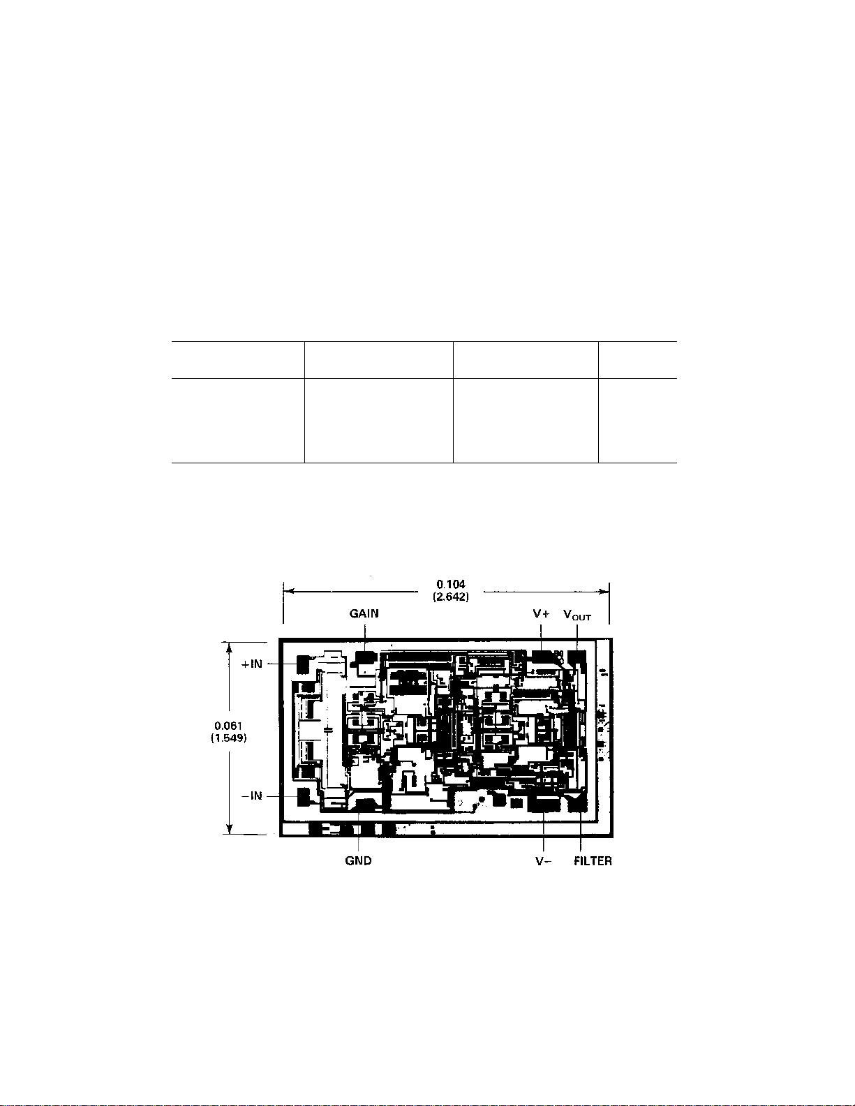
METALIZATION PHOTOGRAPH
Dimensions shown in inches and (mm).
REV. C–4–
Loading...