


Analog Devices AD590, AD590MH, AD590LH, AD590LF, AD590KH Datasheet
...a |
Two-Terminal IC |
|
Temperature Transducer |
||
|
|
|
|
|
AD590 |
|
|
|
|
FEATURES |
PIN DESIGNATIONS |
|
Linear Current Output: 1 mA/K |
|
|
Wide Range: –558C to +1508C |
|
|
Probe Compatible Ceramic Sensor Package |
|
|
Two Terminal Device: Voltage In/Current Out |
|
|
Laser Trimmed to 60.58C Calibration Accuracy (AD590M) |
|
|
Excellent Linearity: 60.38C Over Full Range (AD590M) |
|
|
Wide Power Supply Range: +4 V to +30 V |
|
|
Sensor Isolation from Case |
|
|
Low Cost |
|
PRODUCT DESCRIPTION
The AD590 is a two-terminal integrated circuit temperature transducer that produces an output current proportional to absolute temperature. For supply voltages between +4 V and +30 V the device acts as a high impedance, constant current regulator passing 1 μA/K. Laser trimming of the chip’s thin-film resistors is used to calibrate the device to 298.2 μA output at 298.2K (+25°C).
The AD590 should be used in any temperature sensing application below +150°C in which conventional electrical temperature sensors are currently employed. The inherent low cost of a monolithic integrated circuit combined with the elimination of support circuitry makes the AD590 an attractive alternative for many temperature measurement situations. Linearization circuitry, precision voltage amplifiers, resistance measuring circuitry and cold junction compensation are not needed in applying the AD590.
In addition to temperature measurement, applications include temperature compensation or correction of discrete components, biasing proportional to absolute temperature, flow
rate measurement, level detection of fluids and anemometry. The AD590 is available in chip form making, it suitable for hybrid circuits and fast temperature measurements in protected environments.
The AD590 is particularly useful in remote sensing applications. The device is insensitive to voltage drops over long lines due to its high impedance current output. Any well insulated twisted pair is sufficient for operation hundreds of feet from the receiving circuitry. The output characteristics also make the AD590 easy to multiplex: the current can be switched by a CMOS multiplexer or the supply voltage can be switched by a logic gate output.
REV. B
Information furnished by Analog Devices is believed to be accurate and reliable. However, no responsibility is assumed by Analog Devices for its use, nor for any infringements of patents or other rights of third parties which may result from its use. No license is granted by implication or otherwise under any patent or patent rights of Analog Devices.
PRODUCT HIGHLIGHTS
1.The AD590 is a calibrated two terminal temperature sensor requiring only a dc voltage supply (+4 V to +30 V). Costly transmitters, filters, lead wire compensation and linearization circuits are all unnecessary in applying the device.
2.State-of-the-art laser trimming at the wafer level in conjunction with extensive final testing ensures that AD590 units are easily interchangeable.
3.Superior interface rejection results from the output being a
current rather than a voltage. In addition, power requirements are low (1.5 mWs @ 5 V @ +25°C.) These features make the AD590 easy to apply as a remote sensor.
4.The high output impedance (>10 MΩ) provides excellent rejection of supply voltage drift and ripple. For instance,
changing the power supply from 5 V to 10 V results in only a 1 μA maximum current change, or 1°C equivalent error.
5.The AD590 is electrically durable: it will withstand a forward voltage up to 44 V and a reverse voltage of 20 V. Hence, supply irregularities or pin reversal will not damage the device.
One Technology Way, P.O. Box 9106, Norwood, MA 02062-9106, U.S.A.
Tel: 617/329-4700 |
World Wide Web Site: http://www.analog.com |
Fax: 617/326-8703 |
© Analog Devices, Inc., 1997 |
AD590–SPECIFICATIONS |
(@ +258C and VS = +5 V unless otherwise noted) |
|
|
|
|
|
|||
Model |
|
|
AD590J |
|
|
AD590K |
|
|
|
|
|
Min |
Typ Max |
|
Min |
Typ Max |
Units |
||
|
|
|
|
|
|
|
|
|
|
ABSOLUTE MAXIMUM RATINGS |
|
|
|
|
|
|
|
|
|
Forward Voltage ( E+ or E–) |
|
|
+44 |
|
|
+44 |
Volts |
||
Reverse Voltage (E+ to E–) |
|
|
–20 |
|
|
–20 |
Volts |
||
Breakdown Voltage (Case E+ or E–) |
|
|
± 200 |
|
|
± 200 |
Volts |
||
Rated Performance Temperature Range1 |
|
–55 |
+150 |
|
–55 |
+150 |
°C |
||
Storage Temperature Range1 |
|
–65 |
+155 |
|
–65 |
+155 |
°C |
||
Lead Temperature (Soldering, 10 sec) |
|
|
+300 |
|
|
+300 |
°C |
||
POWER SUPPLY |
|
|
|
|
|
|
|
|
|
Operating Voltage Range |
|
+4 |
+30 |
|
+4 |
+30 |
Volts |
||
|
|
|
|
|
|
|
|
|
|
OUTPUT |
|
|
|
|
|
|
|
|
|
Nominal Current Output @ +25°C (298.2K) |
|
|
298.2 |
|
|
298.2 |
mA |
||
Nominal Temperature Coefficient |
|
|
1 |
|
|
1 |
mA/K |
||
Calibration Error @ +25°C |
|
|
65.0 |
|
|
62.5 |
°C |
||
Absolute Error (Over Rated Performance Temperature Range) |
|
610 |
|
|
65.5 |
°C |
|||
Without External Calibration Adjustment |
|
|
|
|
|||||
With +25°C Calibration Error Set to Zero |
|
|
63.0 |
|
|
62.0 |
°C |
||
Nonlinearity |
|
|
61.5 |
|
|
60.8 |
°C |
||
Repeatability2 |
|
|
± 0.1 |
|
|
± 0.1 |
°C |
||
Long-Term Drift3 |
|
|
± 0.1 |
|
|
± 0.1 |
°C |
||
Current Noise |
|
|
40 |
|
|
40 |
pA/Ö |
Hz |
|
Power Supply Rejection |
|
|
|
|
|
|
|
|
|
+4 V £ VS £ +5 V |
|
|
0.5 |
|
|
0.5 |
mA/V |
||
+5 V £ VS £ +15 V |
|
|
0.2 |
|
|
0.2 |
mV/V |
||
+15 V £ VS £ +30 V |
|
|
0.1 |
|
|
0.1 |
mA/V |
||
Case Isolation to Either Lead |
|
|
1010 |
|
|
1010 |
W |
||
Effective Shunt Capacitance |
|
|
100 |
|
|
100 |
pF |
||
Electrical Turn-On Time |
|
|
20 |
|
|
20 |
ms |
||
Reverse Bias Leakage Current4 |
|
|
|
|
|
|
|
|
|
(Reverse Voltage = 10 V) |
|
|
10 |
|
|
10 |
pA |
||
|
|
|
|
|
|
|
|
|
|
PACKAGE OPTIONS |
|
|
|
|
|
|
|
|
|
TO-52 (H-03A) |
|
|
AD590JH |
|
|
AD590KH |
|
|
|
Flatpack (F-2A) |
|
|
AD590JF |
|
|
AD590KF |
|
|
|
|
|
|
|
|
|
|
|
|
|
NOTES
1The AD590 has been used at –100°C and +200°C for short periods of measurement with no physical damage to the device. However, the absolute errors specified apply to only the rated performance temperature range.
2Maximum deviation between +25°C readings after temperature cycling between –55°C and +150°C; guaranteed not tested. 3Conditions: constant +5 V, constant +125°C; guaranteed, not tested.
4Leakage current doubles every 10°C.
Specifications subject to change without notice.
Specifications shown in boldface are tested on all production units at final electrical test. Results from those tests are used to calculate outgoing quality levels. All min and max specifications are guaranteed, although only those shown in boldface are tested on all production units.
–2– |
REV. B |
|
|
|
|
|
AD590 |
|||
Model |
|
AD590L |
|
AD590M |
|
|
|
|
|
Min |
Typ Max |
Min |
Typ Max |
|
Units |
||
|
|
|
|
|
|
|
|
|
ABSOLUTE MAXIMUM RATINGS |
|
|
|
|
|
|
|
|
Forward Voltage ( E+ or E–) |
|
+44 |
|
+44 |
|
Volts |
||
Reverse Voltage (E+ to E–) |
|
–20 |
|
–20 |
|
Volts |
||
Breakdown Voltage (Case to E+ or E–) |
|
± 200 |
|
± 200 |
|
Volts |
||
Rated Performance Temperature Range1 |
–55 |
+150 |
–55 |
+150 |
|
°C |
||
Storage Temperature Range1 |
–65 |
+155 |
–65 |
+155 |
|
°C |
||
Lead Temperature (Soldering, 10 sec) |
|
+300 |
|
+300 |
|
°C |
||
POWER SUPPLY |
|
|
|
|
|
|
|
|
Operating Voltage Range |
+4 |
+30 |
+4 |
+30 |
|
Volts |
||
|
|
|
|
|
|
|
|
|
OUTPUT |
|
|
|
|
|
|
|
|
Nominal Current Output @ +25°C (298.2K) |
|
298.2 |
|
298.2 |
|
mA |
||
Nominal Temperature Coefficient |
|
1 |
|
1 |
|
mA/K |
||
Calibration Error @ +25°C |
|
61.0 |
|
60.5 |
|
°C |
||
Absolute Error (Over Rated Performance Temperature Range) |
|
63.0 |
|
61.7 |
|
°C |
||
Without External Calibration Adjustment |
|
|
|
|||||
With ± 25°C Calibration Error Set to Zero |
|
61.6 |
|
61.0 |
|
°C |
||
Nonlinearity |
|
60.4 |
|
60.3 |
|
°C |
||
Repeatability2 |
|
± 0.1 |
|
± 0.1 |
|
°C |
||
Long-Term Drift3 |
|
± 0.1 |
|
± 0.1 |
|
°C |
||
Current Noise |
|
40 |
|
40 |
|
pA/Ö |
Hz |
|
Power Supply Rejection |
|
|
|
|
|
|
|
|
+4 V £ VS £ +5 V |
|
0.5 |
|
0.5 |
|
mA/V |
||
+5 V £ VS £ +15 V |
|
0.2 |
|
0.2 |
|
mA/V |
||
+15 V £ VS £ +30 V |
|
0.1 |
|
0.1 |
|
mA/V |
||
Case Isolation to Either Lead |
|
1010 |
|
1010 |
|
W |
||
Effective Shunt Capacitance |
|
100 |
|
100 |
|
pF |
||
Electrical Turn-On Time |
|
20 |
|
20 |
|
ms |
||
Reverse Bias Leakage Current4 |
|
|
|
|
|
|
|
|
(Reverse Voltage = 10 V) |
|
10 |
|
10 |
|
pA |
||
|
|
|
|
|
|
|
|
|
PACKAGE OPTIONS |
|
|
|
|
|
|
|
|
TO-52 (H-03A) |
|
AD590LH |
|
AD590MH |
|
|
|
|
Flatpack (F-2A) |
|
AD590LF |
|
AD590MF |
|
|
|
|
|
|
|
|
|
|
|
|
|
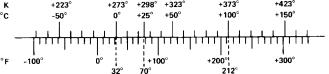
TEMPERATURE SCALE CONVERSION EQUATIONS
°C = |
5 |
(° F – 32) |
K = °C +273.15 |
|
|||
9 |
|
|
|
° F = |
9 |
°C + 32 |
° R = ° F +459.7 |
|
|||
5 |
|
|
|
REV. B |
–3– |

AD590
The 590H has 60 μ inches of gold plating on its Kovar leads and Kovar header. A resistance welder is used to seal the nickel cap to the header. The AD590 chip is eutectically mounted to the header and ultrasonically bonded to with 1 MIL aluminum wire. Kovar composition: 53% iron nominal; 29% ±1% nickel; 17% ± 1% cobalt; 0.65% manganese max; 0.20% silicon max; 0.10% aluminum max; 0.10% magnesium max; 0.10% zirconium max; 0.10% titanium max; 0.06% carbon max.
The 590F is a ceramic package with gold plating on its Kovar leads, Kovar lid, and chip cavity. Solder of 80/20 Au/Sn composition is used for the 1.5 mil thick solder ring under the lid. The chip cavity has a nickel underlay between the metalization
and the gold plating. The AD590 chip is eutectically mounted in the chip cavity at 410°C and ultrasonically bonded to with 1
mil aluminum wire. Note that the chip is in direct contact with the ceramic base, not the metal lid. When using the AD590 in die form, the chip substrate must be kept electrically isolated, (floating), for correct circuit operation.
METALIZATION DIAGRAM
In the AD590, this PTAT voltage is converted to a PTAT current by low temperature coefficient thin-film resistors. The total current of the device is then forced to be a multiple of this PTAT current. Referring to Figure 1, the schematic diagram of the AD590, Q8 and Q11 are the transistors that produce the PTAT voltage. R5 and R6 convert the voltage to current. Q10, whose collector current tracks the colletor currents in Q9 and Q11, supplies all the bias and substrate leakage current for the rest of the circuit, forcing the total current to be PTAT. R5 and
R6 are laser trimmed on the wafer to calibrate the device at +25°C.
Figure 2 shows the typical V–I characteristic of the circuit at +25°C and the temperature extremes.
Figure 1. Schematic Diagram
CIRCUIT DESCRIPTION1
The AD590 uses a fundamental property of the silicon transistors from which it is made to realize its temperature proportional characteristic: if two identical transistors are operated at a constant ratio of collector current densities, r, then the difference in their base-emitter voltage will be (kT/q)(In r). Since both k, Boltzman’s constant and q, the charge of an electron, are constant, the resulting voltage is directly proportional to absolute temperature (PTAT).
Figure 2. V–I Plot
1For a more detailed circuit description see M.P. Timko, “A Two-Terminal IC Temperature Transducer,” IEEE J. Solid State Circuits, Vol. SC-11, p. 784-788, Dec. 1976.
–4– |
REV. B |
 Loading...