


a |
16-Bit Monotonic |
|
Voltage Output D/A Converter |
||
|
|
AD569 |
FEATURES
Guaranteed 16-Bit Monotonicity Monolithic BiMOS II Construction 60.01% Typical Nonlinearity
8- and 16-Bit Bus Compatibility
3 ms Settling to 16 Bits
Low Drift
Low Power
Low Noise
APPLICATIONS
Robotics
Closed-Loop Positioning
High-Resolution ADCs
Microprocessor-Based Process Control
MIL-STD-883 Compliant Versions Available
PRODUCT DESCRIPTION
The AD569 is a monolithic 16-bit digital-to-analog converter (DAC) manufactured in Analog Devices’ BiMOS II process. BiMOS II allows the fabrication of low power CMOS logic functions on the same chip as high precision bipolar linear circuitry. The AD569 chip includes two resistor strings, selector switches decoding logic, buffer amplifiers, and double-buffered input latches.
The AD569’s voltage-segmented architecture insures 16-bit monotonicity over time and temperature. Integral nonlinearity is maintained at ±0.01%, while differential nonlinearity is
±0.0004%. The on-chip, high-speed buffer amplifiers provide a voltage output settling time of 3 μs to within ±0.001% for a full-scale step.
The reference input voltage which determines the output range can be either unipolar or bipolar. Nominal reference range is
±5 V and separate reference force and sense connections are provided for high accuracy applications. The AD569 can operate with an ac reference in multiplying applications.
Data may be loaded into the AD569’s input latches from 8- and 16-bit buses. The double-buffered structure simplifies 8-bit bus interfacing and allows multiple DACs to be loaded asynchronously and updated simultaneously. Four TTL/LSTTL/5 V CMOS-compatible signals control the latches: CS, LBE, HBE, and LDAC
The AD569 is available in five grades: J and K versions are specified from 0°C to +70°C and are packaged in a 28-pin plastic DIP and 28-pin PLCC package; AD and BD versions are specified from –25°C to +85°C and are packaged in a 28-pin ceramic DIP. The SD version, also in a 28-pin ceramic DIP, is specified from –55°C to +125°C.
REV. A
Information furnished by Analog Devices is believed to be accurate and reliable. However, no responsibility is assumed by Analog Devices for its use, nor for any infringements of patents or other rights of third parties which may result from its use. No license is granted by implication or otherwise under any patent or patent rights of Analog Devices.
FUNCTIONAL BLOCK DIAGRAM
PRODUCT HIGHLIGHTS
1.Monotonicity to 16 bits is insured by the AD569’s voltagesegmented architecture.
2.The output range is ratiometric to an external reference or ac signal. Gain error and gain drift of the AD569 are negligible.
3.The AD569’s versatile data input structure allows loading from 8- and 16-bit buses.
4. The on-chip output buffer amplifier can supply ±5 V into a 1 kΩ load, and can drive capacitive loads of up to 1000 pF.
5.Kelvin connections to the reference inputs preserve the gain and offset accuracy of the transfer function in the presence of wiring resistances and ground currents.
6.The AD569 is available in versions compliant with MIL-STD-
883.Refer to the Analog Devices Military Products Databook or current AD569/883B data sheet for detailed specifications.
One Technology Way, P.O. Box 9106, Norwood, MA 02062-9106, U.S.A. Tel: 617/329-4700 Fax: 617/326-8703
AD569–SPECIFICATIONS (TA = +258C, +VS = +12 V, –VS = –12 V, +VREF = +5 V, –VREF = –5 V, unless otherwise noted.)
Model |
AD569JN/JP/AD |
AD569KN/KP/BD |
|
AD569SD |
|
|
||||
Parameter |
Min |
Typ |
Max |
Min |
Typ |
Max |
Min |
Typ |
Max |
Units |
|
|
|
|
|
|
|
|
|
|
|
RESOLUTION |
|
|
16 |
|
|
16 |
|
|
16 |
Bits |
LOGIC INPUTS |
2.0 |
|
5.5 |
2.0 |
|
5.5 |
2.0 |
|
5.5 |
|
VIH(Logic “l”) |
|
|
|
Volts |
||||||
VIL (Logic “0”) |
0 |
|
0.8 |
0 |
|
0.8 |
0 |
|
0.8 |
Volts |
IIH (VIH = 5.5 V) |
|
|
10 |
|
|
10 |
|
|
10 |
mA |
IIL (VIL = 0 V) |
|
|
10 |
|
|
10 |
|
|
10 |
mA |
TRANSFER FUNCTION |
|
|
|
|
|
|
|
|
|
|
CHARACTERISTICS |
|
± 0.02 |
60.04 |
|
± 0.01 |
60.024 |
|
|
60.04 |
% FSR1 |
Integral Nonlinearity |
|
|
|
|
||||||
TMIN to TMAX |
|
± 0.02 |
60.04 |
|
± 0.020 |
60.024 |
|
|
60.04 |
% FSR |
Differential Nonlinearity |
|
± 1/2 |
61 |
|
± 1/4 |
61/2 |
|
|
61 |
LSB |
TMIN to TMAX |
|
± 1/2 |
61 |
|
± 1/2 |
61 |
|
|
61 |
LSB |
Unipolar Offset2 |
|
|
6500 |
|
|
6350 |
|
|
6500 |
mV |
TMIN to TMAX |
|
|
6750 |
|
|
6450 |
|
|
6750 |
mV |
Bipolar Offset2 |
|
|
6500 |
|
|
6350 |
|
|
6500 |
mV |
TMIN to TMAX |
|
|
6750 |
|
|
6450 |
|
|
6750 |
mV |
Full Scale Error2 |
|
|
6350 |
|
|
6350 |
|
|
6350 |
mV |
TMIN to TMAX |
|
|
6750 |
|
|
6750 |
|
|
6750 |
mV |
Bipolar Zero2 |
|
|
60.04 |
|
|
60.024 |
|
|
60.04 |
% FSR |
TMIN to TMAX |
|
|
60.04 |
|
|
60.024 |
|
|
60.04 |
% FSR |
REFERENCE INPUT |
|
|
|
|
|
|
|
|
|
|
+VREF Range3 |
–5 |
|
+5 |
–5 |
|
+5 |
–5 |
|
+5 |
Volts |
–VREF Range |
–5 |
|
+5 |
–5 |
|
+5 |
–5 |
|
+5 |
Volts |
Resistance |
15 |
20 |
25 |
15 |
20 |
25 |
15 |
20 |
25 |
kW4 |
OUTPUT CHARACTERISTICS |
|
|
|
|
|
|
|
|
|
|
Voltage |
–5 |
|
+5 |
–5 |
|
+5 |
–5 |
|
+5 |
Volts |
Capacitive Load |
|
|
1000 |
|
|
1000 |
|
|
1000 |
pF |
Resistive Load |
1 |
|
|
1 |
|
|
1 |
|
|
kW |
Short Circuit Current |
|
10 |
|
|
10 |
|
|
10 |
|
mA |
|
|
|
|
|
|
|
|
|
|
|
POWER SUPPLIES |
|
|
|
|
|
|
|
|
|
|
Voltage |
+10.8 |
|
+13.2 |
+10.8 |
|
+13.2 |
+10.8 |
|
+13.2 |
|
+VS |
+12 |
+12 |
+12 |
Volts |
||||||
–VS |
–10.8 |
–12 |
–13.2 |
–10.8 |
–12 |
–13.2 |
–10.8 |
–12 |
–13.2 |
Volts |
Current |
|
|
|
|
|
|
|
|
|
|
+IS |
|
+9 |
+13 |
|
+9 |
+13 |
|
+9 |
+13 |
mA |
–IS |
|
–9 |
–13 |
|
–9 |
–13 |
|
–9 |
–13 |
mA |
Power Supply Sensitivity5 |
|
|
|
|
|
|
|
|
|
|
+10.8 V £ +VS £ +13.2 V |
|
± 0.5 |
62 |
|
± 0.5 |
62 |
|
± 0.5 |
62 |
ppm/% |
–10.8 V ³ –VS ³ –13.2 V |
|
± 1 |
63 |
|
± 1 |
63 |
|
± 1 |
63 |
ppm/% |
TEMPERATURE RANGE |
|
|
|
|
|
|
|
|
|
|
Specified |
|
|
|
|
|
|
|
|
|
°C |
JN, KN, JP, KP |
0 |
|
+70 |
0 |
|
+70 |
|
|
|
|
AD, BD |
–25 |
|
+85 |
–25 |
|
+85 |
|
|
|
°C |
SD |
|
|
|
|
|
|
–55 |
|
+125 |
°C |
Storage |
|
|
|
|
|
|
|
|
|
°C |
JN, KN, JP, KP |
–65 |
|
+150 |
–65 |
|
+150 |
|
|
|
|
AD, BD, SD |
–65 |
|
+150 |
–65 |
|
+150 |
–65 |
|
+150 |
°C |
|
|
|
|
|
|
|
|
|
|
|
NOTES
1FSR stands for Full-Scale Range, and is 10 V for a –5 V to +5 V span. 2Refer to Definitions section.
3For operation with supplies other than ± 12 V, refer to the Power Supply and Reference Voltage Range Section. 4Measured between +VREF Force and –VREF Force.
5Sensitivity of Full-Scale Error due to changes in +VS and sensitivity of Offset to changes in –VS.
Specifications subject to change without notice.
Specifications shown in boldface are tested on all production units at final electrical test. Results from those tests are used to calculate outgoing quality levels. All min and max specifications are guaranteed, although only those shown in boldface are tested on all production units.
–2– |
REV. A |

AD569
AC PERFORMANCE CHARACTERISTICS
These characteristics are included for Design Guidance Only and are not subject to test. +VS = +12 V; –VS = –12 V; +VREF = +5 V; –VREF = –5 V excepts where stated.
Parameter |
|
|
Limit |
|
|
|
Units |
|
|
Test Conditions/Comments |
|||||||||||||||
|
|
|
|
|
|
|
|
|
|
|
|
|
|
|
|
|
|
|
|
|
|
|
|
|
|
Output Voltage Settling |
5 |
|
|
|
|
μs max |
|
|
No Load Applied |
||||||||||||||||
(Time to ±0.001% FS |
3 |
|
|
|
|
μs typ |
|
|
(DAC output measured from falling edge of |
|
.) |
||||||||||||||
LDAC |
|||||||||||||||||||||||||
For FS Step) |
|
|
6 |
|
|
|
|
μs max |
|
|
VOUT Load = 1 kΩ, CLOAD = 1000 pF. |
||||||||||||||
|
|
|
4 |
|
|
|
|
μs typ |
|
|
(DAC output measured from falling edge of |
|
) |
||||||||||||
|
|
|
LDAC. |
||||||||||||||||||||||
Digital-to-Analog Glitch |
500 |
|
|
|
|
nV-sec typ |
|
|
Measured with VREF = 0 V. DAC registers alternatively loaded |
||||||||||||||||
Impulse |
|
|
|
|
|
|
|
|
|
|
|
|
|
|
|
|
|
|
with input codes of 8000H and 0FFFH (worst-case |
||||||
|
|
|
|
|
|
|
|
|
|
|
|
|
|
|
|
|
|
|
transition). Load = 1 kΩ. |
||||||
Multiplying Feedthrough |
–100 |
|
|
|
dB max |
|
|
+VREF = 1 V rms 10 kHz sine wave, |
|||||||||||||||||
|
|
|
|
|
|
|
|
|
|
|
|
|
|
|
|
|
|
|
–VREF = 0 V |
||||||
Output Noise Voltage |
40 |
|
|
|
|
nV/Ï |
|
|
typ |
|
|
Measured between VOUT and –VREF |
|||||||||||||
Hz |
|||||||||||||||||||||||||
Density (1 kHz-1 MHz) |
|
|
|
|
|
|
|
|
|
|
|
|
|
|
|
|
|
|
|
|
|
|
|
||
|
|
|
|
|
|
|
|
|
|
|
|
|
|
|
|
|
|
|
|
|
|||||
TIMING CHARACTERISTICS (+VS = +12 V, –VS = –12 V, VIH = 2.4 V, VIL = 0.4 V,TMIN to TMAX) |
|||||||||||||||||||||||||
Parameter |
Limit |
|
Units |
|
|
|
Test Conditions/Comments |
|
|||||||||||||||||
|
|
|
|
|
|
|
|
|
|
|
|
|
|
|
|
|
|
|
|
||||||
Case A |
|
|
|
|
150 ns Pulse on |
|
, |
|
, and |
|
|
||||||||||||||
|
|
|
|
HBE |
LBE |
LDAC |
|||||||||||||||||||
tWC |
|
|
|
|
|
THS = 140 ns min, THH = 10 ns min |
|||||||||||||||||||
120 |
|
ns min |
|
|
CS |
Pulse Width |
|
|
|
|
|
|
|
|
|||||||||||
tSC |
60 |
|
ns min |
|
|
CS |
Data Setup Time |
|
|
|
|
|
|
|
|
||||||||||
tHC |
20 |
|
ns min |
|
|
CS Data Hold Time |
|
|
|
|
|
|
|
|
|||||||||||
Case B |
|
|
|
|
|
None |
|
|
|
|
|
|
|
|
|||||||||||
tWB |
70 |
|
ns min |
|
|
|
|
, |
|
|
Pulse Width |
||||||||||||||
|
HBE |
LBE |
|||||||||||||||||||||||
tSB |
80 |
|
ns min |
|
|
HBE |
, |
LBE |
Data Setup Time |
||||||||||||||||
tHB |
20 |
|
ns min |
|
|
HBE |
, |
LBE |
Data Hold Time |
||||||||||||||||
tSCS |
120 |
|
ns min |
|
|
CS Setup Time |
|
|
|
|
|
|
|
|
|||||||||||
tHCS |
10 |
|
ns min |
|
|
CS |
Hold Time |
|
|
|
|
|
|
|
|
||||||||||
tWD |
120 |
|
ns min |
|
|
LDAC |
Pulse Width |
|
|
|
|
|
|
|
|
||||||||||
Case C |
|
|
|
|
|
None |
|
|
|
Figure 2a. AD569 Timing Diagram – Case B |
|||||||||||||||
tWB |
|
|
|
|
|
|
|
|
|
|
|
|
|
|
|
|
|
|
|
|
|||||
120 |
|
ns min |
|
|
|
HBE |
, |
LBE |
Pulse Width |
||||||||||||||||
tSB |
80 |
|
ns min |
|
|
HBE |
, |
LBE |
Data Setup Time |
||||||||||||||||
tHB |
20 |
|
ns min |
|
|
HBE, LBE Data Hold Time |
|||||||||||||||||||
tSCS |
120 |
|
ns min |
|
|
CS |
Setup Time |
|
|
|
|
|
|
|
|
||||||||||
tHCS |
10 |
|
ns min |
|
|
CS |
Hold Time |
|
|
|
|
|
|
|
|
||||||||||
Figure 1. AD569 Timing Diagram – Case A |
Figure 2b. AD569 Timing Diagram – Case C |
REV. A |
–3– |
AD569
ABSOLUTE MAXIMUM RATINGS* |
|
|
Power Dissipation (Any Package) . . . . . . . . . |
. . . . . . 1000 mW |
|
(TA = +25°C unless otherwise noted) |
|
|
Operating Temperature Range |
|
|
+VS (Pin 1) to GND (Pin 18) . . . . . . |
. . . . . . . |
. +18 V, –0.3 V |
Commercial Plastic (JN, KN, JP, KP Versions) 0°C to +70°C |
||
–VS (Pin 28) to GND (Pin 18) . . . . . . . |
. . . . . . . |
–18 V, +0.3 V |
Industrial Ceramic (AD, BD Versions) . . . . –25°C to +85°C |
||
+VS (Pin 1) to –VS (Pin 28) . . . . . . . . . |
. . . . . . |
+26.4 V, –0.3 V |
Extended Ceramic (SD Versions) . . . . . . . |
–55°C to +125°C |
|
Digital Inputs |
|
|
Storage Temperature . . . . . . . . . . . . . . . . . . . |
–65°C to +150°C |
|
(Pins 4-14, 19-27) to GND (Pin 18) |
. . . . . . . |
. . +VS, –0.3 V |
Lead Temperature Range (Soldering, 10 secs) |
. . . . . . . +300°C |
|
+VREF Force (Pin 3) to +VREF Sense (Pin 2) . . . |
. . . . . ±16.5 V |
|
|
||
–VREF Force (Pin 15) to –VREF Sense (Pin 16) . . |
. . . . . ±16.5 V |
*Stresses above those listed under “Absolute Maximum Ratings” may cause |
|||
VREF Force (Pins 3, 15) to GND (Pin 18) |
±VS |
permanent damage to the device. This is a stress rating only and functional |
|||
operation of the device at these or any other conditions above those indicated in the |
|||||
VREF Sense (Pins 2, 16) to GND (Pin 18) |
±VS |
||||
operational sections of this specification is not implied. Exposure to absolute |
|||||
. . . . . . . . . . . . . . . . . .VOUT (Pin 17) |
Indefinite Short to GND |
maximum rating conditions for extended periods may affect device reliability. |
|||
Momentary Short to +VS, –VS
ESD SENSITIVITY |
|
|
|
The AD569 features input protection circuitry consisting of large “distributed” diodes and polysilicon |
|
||
series resistors to dissipate both high-energy discharges (Human Body Model) and fast, low-energy |
|
||
pulses (Charged Device Model). Per Method 3015.2 of MIL-STD-883C, the AD569 has been |
|
||
classified as a Category A device. |
WARNING! |
||
Proper ESD precautions are strongly recommended to avoid functional damage or performance |
|||
|
|||
degradation. Charges as high as 4000 volts readily accumulate on the human body and test equipment |
|
||
and discharge without detection. Unused devices must be stored in conductive foam or shunts, and |
ESD SENSITIVE DEVICE |
||
the foam should be discharged to the destination socket before devices are removed. For further |
|
||
information on ESD precautions, refer to Analog Devices’ ESD Prevention Manual. |
|
||
|
|
|
|
|
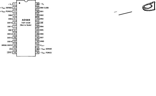
PIN DESIGNATIONS |
|
|
ORDERING GUIDE
|
Integral Nonlinearity |
Differential Nonlinearity |
Temperature |
Package |
||
Model1 |
+258C |
TMIN–TMAX |
+258C |
TMIN–TMAX |
Range |
Option2 |
AD569JN |
±0.04% |
±0.04% |
±1 LSB |
±1 LSB |
0°C to +70°C |
N-28 |
AD569JP |
±0.04% |
±0.04% |
±1 LSB |
±1 LSB |
0°C to +70°C |
P-28A |
AD569KN |
±0.024% |
±0.024% |
±1/2 LSB |
±1 LSB |
0°C to +70°C |
N-28 |
AD569KP |
±0.024% |
±0.024% |
±1/2 LSB |
±1 LSB |
0°C to +70°C |
P-28A |
AD569AD |
±0.04% |
±0.04% |
±1 LSB |
±1 LSB |
–25°C to +85°C |
D-28 |
AD569BD |
±0.024% |
±0.024% |
±1/2 LSB |
±1 LSB |
–25°C to +85°C |
D-28 |
AD569SD |
±0.04% |
±0.04% |
±1 LSB |
±1 LSB |
–55°C to +125°C |
D-28 |
|
|
|
|
|
|
|
NOTES
1For details on grade and package offerings screened in accordance with MIL-STD-883, refer to the Analog Devices Military Products Databook or current AD569/883B data sheet.
2D = Ceramic DIP; N = Plastic DIP; P = Plastic Leaded Chip Carrier.
–4– |
REV. A |
 Loading...