


 Loading...
Data Sheet
FEATURES
10 MHz multiplying bandwidth INL of ±0.25 LSB @ 8 bits
20-lead and 24-lead TSSOP packages
2.5 V to 5.5 V supply operation ±10 V reference input
21.3 MSPS update rate
Extended temperature range: −40°C to +125°C 4-quadrant multiplication
Power-on reset
0.5 μA typical current consumption Guaranteed monotonic
Readback function AD7528 upgrade (AD5428) AD7547 upgrade (AD5447)
APPLICATIONS
Portable battery-powered applications Waveform generators
Analog processing Instrumentation applications
Programmable amplifiers and attenuators Digitally controlled calibration Programmable filters and oscillators Composite video
Ultrasound
Gain, offset, and voltage trimming
Dual 8-/10-/12-Bit, High Bandwidth, Multiplying DACs with Parallel Interface AD5428/AD5440/AD5447
GENERAL DESCRIPTION
The AD5428/AD5440/AD54471 are CMOS, 8-, 10-, and 12-bit, dual-channel, current output digital-to-analog converters (DACs), respectively. These devices operate from a 2.5 V to 5.5 V power supply, making them suited to battery-powered and other applications.
As a result of being manufactured on a CMOS submicron process, they offer excellent 4-quadrant multiplication characteristics, with large signal multiplying bandwidths of up to 10 MHz.
The DACs use data readback, allowing the user to read the contents of the DAC register via the DB pins. On power-up, the internal register and latches are filled with 0s, and the DAC outputs are at zero scale.
The applied external reference input voltage (VREF) determines the full-scale output current. An integrated feedback resistor (RFB) provides temperature tracking and full-scale voltage output when combined with an external I-to-V precision amplifier.
The AD5428 is available in a small 20-lead TSSOP package, and the AD5440/AD5447 DACs are available in small 24-lead TSSOP packages.
1 U.S. Patent Number 5,689,257.
FUNCTIONAL BLOCK DIAGRAM
|
|
|
|
VREFA |
|
|
|
|
AD5428/AD5440/AD5447 |
|
|
|
|
|
VDD |
|
|
|
R |
RFBA |
|
|
|
|
|
||
DATA |
DB0 |
INPUT |
LATCH |
8-/10-/12-BIT |
|
IOUTA |
INPUTS |
|
|
|
|||
|
DB7 |
BUFFER |
|
R-2R DAC A |
|
|
|
|
|
|
|
||
|
|
|
|
|
|
|
|
DB9 |
|
|
|
|
|
|
DB11 |
|
|
|
|
AGND |
|
|
|
|
|
|
|
DAC A/B |
|
|
|
R |
|
|
|
|
CONTROL |
|
|
RFBB |
|
|
CS |
|
|
|
||
|
LOGIC |
|
|
|
|
|
|
R/W |
|
LATCH |
8-/10-/12-BIT |
|
IOUTB |
|
|
|
|
R-2R DAC B |
|
|
|
DGND |
|
|
|
|
|
|
|
POWER-ON |
|
|
|
|
|
|
RESET |
|
|
|
|
|
|
|
|
VREFB |
|
04462-001 |
|
|
|
|
|
|
|
|
|
Figure 1. AD5428/AD5440/AD5447 |
|
|
||
Rev. C
InformationfurnishedbyAnalogDevicesisbelievedtobeaccurateandreliable.However,no responsibilityisassumedbyAnalogDevicesforitsuse,norforanyinfringementsofpatentsorother rightsofthirdpartiesthatmayresultfromitsuse.Specificationssubjecttochangewithoutnotice.No licenseisgrantedbyimplicationorotherwiseunderanypatentorpatentrightsofAnalogDevices. Trademarksandregisteredtrademarksarethepropertyoftheirrespectiveowners.
One Technology Way, P.O. Box 9106, Norwood, MA 02062-9106, U.S.A. Tel: 781.329.4700 www.analog.com Fax: 781.461.3113 ©2004–2011 Analog Devices, Inc. All rights reserved.

AD5428/AD5440/AD5447 |
Data Sheet |
|
|
TABLE OF CONTENTS |
|
Specifications..................................................................................... |
3 |
Timing Characteristics ................................................................ |
5 |
Absolute Maximum Ratings............................................................ |
6 |
ESD Caution.................................................................................. |
6 |
Pin Configurations and Function Descriptions ........................... |
7 |
Typical Performance Characteristics ........................................... |
10 |
Terminology .................................................................................... |
15 |
General Description ....................................................................... |
16 |
DAC Section................................................................................ |
16 |
Circuit Operation ....................................................................... |
16 |
Single-Supply Applications ....................................................... |
19 |
Adding Gain................................................................................ |
19 |
REVISION HISTORY |
|
8/11—Rev. B to Rev. C |
|
Changes to CS Pin Description, Table 6........................................ |
9 |
3/11—Rev. A to Rev. B |
|
Changes to Evaluation Board For the AD5447 Section ............ |
23 |
Changes to Figure 47 Caption....................................................... |
24 |
Changes to Figure 49...................................................................... |
25 |
Change to U1 Description in Table 12......................................... |
27 |
Change to Ordering Guide............................................................ |
29 |
7/05—Rev. 0 to Rev. A |
|
Changed Pin DAC A/B to DAC A/B................................ |
Universal |
Changes to Features List .................................................................. |
1 |
Changes to Specifications ................................................................ |
3 |
Changes to Timing Characteristics ................................................ |
5 |
Change to Figure 2 ........................................................................... |
5 |
Change to Absolute Maximum Ratings Section........................... |
6 |
Change to Figure 13, Figure 14, and Figure 18........................... |
11 |
Change to Figure 32 Through Figure 34 ..................................... |
14 |
Divider or Programmable Gain Element................................ |
20 |
Reference Selection .................................................................... |
20 |
Amplifier Selection .................................................................... |
20 |
Parallel Interface......................................................................... |
22 |
Microprocessor Interfacing....................................................... |
22 |
PCB Layout and Power Supply Decoupling ........................... |
23 |
Evaluation Board for the AD5447............................................ |
23 |
Power Supplies for the Evaluation Board................................ |
23 |
Bill of Materials............................................................................... |
27 |
Overview of AD54xx Devices....................................................... |
28 |
Outline Dimensions ....................................................................... |
29 |
Ordering Guide .......................................................................... |
29 |
Changes to General Description Section .................................... |
16 |
Changes to Figure 37...................................................................... |
16 |
Changes to Single-Supply Applications Section......................... |
19 |
Changes to Figure 40 Through Figure 42.................................... |
19 |
Changes to Divider or Programmable Gain Element Section.... |
20 |
Changes to Figure 43...................................................................... |
20 |
Changes to Table 9 Through Table 11 ......................................... |
21 |
Changes to Microprocessor Interfacing Section ........................ |
22 |
Added Figure 44 Through Figure 46 ........................................... |
22 |
Added 8xC51-to-AD5428/AD5440/AD5447 |
|
Interface Section ........................................................................ |
22 |
Added ADSP-BF5xx-to-AD5428/AD5440/AD5447 |
|
Interface Section ........................................................................ |
22 |
Changes to Power Supplies for the Evaluation Board Section.... |
23 |
Changes to Table 13 ....................................................................... |
28 |
Updated Outline Dimensions....................................................... |
29 |
Changes to Ordering Guide .......................................................... |
29 |
7/04—Revision 0: Initial Version |
|
Rev. C | Page 2 of 32

Data Sheet |
AD5428/AD5440/AD5447 |
|
|
SPECIFICATIONS1
VDD = 2.5 V to 5.5 V, VREF = 10 V, IOUT2 = 0 V. Temperature range for Y version: −40°C to +125°C. All specifications TMIN to TMAX, unless otherwise noted. DC performance is measured with OP177, and ac performance is measured with AD8038, unless otherwise noted.
Table 1.
Parameter |
Min |
Typ |
Max |
Unit |
|
|
|
|
|
STATIC PERFORMANCE |
|
|
|
|
AD5428 |
|
|
|
|
Resolution |
|
|
8 |
Bits |
Relative Accuracy |
|
|
±0.25 |
LSB |
Differential Nonlinearity |
|
|
±1 |
LSB |
AD5440 |
|
|
|
|
Resolution |
|
|
10 |
Bits |
Relative Accuracy |
|
|
±0.5 |
LSB |
Differential Nonlinearity |
|
|
±1 |
LSB |
AD5447 |
|
|
|
|
Resolution |
|
|
12 |
Bits |
Relative Accuracy |
|
|
±1 |
LSB |
Differential Nonlinearity |
|
|
–1/+2 |
LSB |
Gain Error |
|
|
±25 |
mV |
Gain Error Temperature Coefficient |
|
±5 |
|
ppm FSR/°C |
Output Leakage Current |
|
|
±5 |
nA |
|
|
|
±15 |
nA |
REFERENCE INPUT |
|
|
|
|
Reference Input Range |
|
±10 |
|
V |
VREFA, VREFB Input Resistance |
8 |
10 |
13 |
kΩ |
VREFA-to-VREFB Input |
|
1.6 |
2.5 |
% |
Resistance Mismatch |
|
|
|
|
Input Capacitance |
|
|
|
|
Code 0 |
|
3.5 |
|
pF |
Code 4095 |
|
3.5 |
|
pF |
DIGITAL INPUTS/OUTPUT |
|
|
|
|
Input High Voltage, VIH |
1.7 |
|
|
V |
|
1.7 |
|
|
V |
Input Low Voltage, VIL |
|
|
0.8 |
V |
|
|
|
0.7 |
V |
Output High Voltage, VOH |
VDD − 1 |
|
|
V |
|
VDD − 0.5 |
|
|
V |
Output Low Voltage, VOL |
|
|
0.4 |
V |
|
|
|
0.4 |
V |
Input Leakage Current, IIL |
|
|
1 |
μA |
Input Capacitance |
|
4 |
10 |
pF |
|
|
|
|
|
DYNAMIC PERFORMANCE |
|
|
|
|
Reference-Multiplying BW |
|
10 |
|
MHz |
Output Voltage Settling Time |
|
|
|
|
Measured to ±1 mV of FS |
|
80 |
120 |
ns |
Measured to ±4 mV of FS |
|
35 |
70 |
ns |
Measured to ±16 mV of FS |
|
30 |
60 |
ns |
Digital Delay |
|
20 |
40 |
ns |
10% to 90% Settling Time |
|
15 |
30 |
ns |
Digital-to-Analog Glitch Impulse |
|
3 |
|
nV-sec |
|
|
|
|
|
Conditions
Guaranteed monotonic
Guaranteed monotonic
Guaranteed monotonic
Data = 0x0000, TA = 25°C
Data = 0x0000
Input resistance TC = –50 ppm/°C Typ = 25°C, max = 125°C
VDD = 3.6 V to 5.5 V VDD = 2.5 V to 3.6 V VDD = 2.7 V to 5.5 V VDD = 2.5 V to 2.7 V
VDD = 4.5 V to 5.5 V, ISOURCE = 200 μA VDD = 2.5 V to 3.6 V, ISOURCE = 200 μA VDD = 4.5 V to 5.5 V, ISINK = 200 μA VDD = 2.5 V to 3.6 V, ISINK = 200 μA
VREF = ±3.5 V p-p, DAC loaded all 1s RLOAD = 100 Ω, CLOAD = 15 pF, VREF = 10 V
DAC latch alternately loaded with 0s and 1s
Interface delay time
Rise and fall times, VREF = 10 V, RLOAD = 100 Ω 1 LSB change around major carry, VREF = 0 V
Rev. C | Page 3 of 32
AD5428/AD5440/AD5447 |
|
|
|
|
|
Data Sheet |
|
|
|
|
|
|
|
|
|
|
|
|
|
|
|
|
|
Parameter |
Min |
Typ |
Max |
Unit |
Conditions |
||
Multiplying Feedthrough Error |
|
|
|
|
DAC latches loaded with all 0s, VREF = ±3.5 V |
||
|
|
|
70 |
dB |
1 MHz |
||
|
|
|
48 |
dB |
10 MHz |
||
Output Capacitance |
|
12 |
17 |
pF |
DAC latches loaded with all 0s |
||
|
|
25 |
30 |
pF |
DAC latches loaded with all 1s |
||
Digital Feedthrough |
|
1 |
|
nV-sec |
|
||
|
|
Feedthrough to DAC output with |
CS |
high and |
|||
|
|
|
|
|
alternate loading of all 0s and all 1s |
||
Output Noise Spectral Density |
|
25 |
|
nV/√Hz |
@ 1 kHz |
||
Analog THD |
|
81 |
|
dB |
VREF = 3.5 V p-p, all 1s loaded, f = 100 kHz |
||
Digital THD |
|
|
|
|
Clock = 10 MHz, VREF = 3.5 V |
||
100 kHz fOUT |
|
61 |
|
dB |
|
|
|
50 kHz fOUT |
|
66 |
|
dB |
|
|
|
SFDR Performance (Wide Band) |
|
|
|
|
AD5447, 65k codes, VREF = 3.5 V |
||
Clock = 10 MHz |
|
|
|
|
|
|
|
500 kHz fOUT |
|
55 |
|
dB |
|
|
|
100 kHz fOUT |
|
63 |
|
dB |
|
|
|
50 kHz fOUT |
|
65 |
|
dB |
|
|
|
Clock = 25 MHz |
|
|
|
|
|
|
|
500 kHz fOUT |
|
50 |
|
dB |
|
|
|
100 kHz fOUT |
|
60 |
|
dB |
|
|
|
50 kHz fOUT |
|
62 |
|
dB |
|
|
|
SFDR Performance (Narrow Band) |
|
|
|
|
AD5447, 65k codes, VREF = 3.5 V |
||
Clock = 10 MHz |
|
|
|
|
|
|
|
500 kHz fOUT |
|
73 |
|
dB |
|
|
|
100 kHz fOUT |
|
80 |
|
dB |
|
|
|
50k Hz fOUT |
|
87 |
|
dB |
|
|
|
Clock = 25 MHz |
|
|
|
|
|
|
|
500 kHz fOUT |
|
70 |
|
dB |
|
|
|
100 kHz fOUT |
|
75 |
|
dB |
|
|
|
50 kHz fOUT |
|
80 |
|
dB |
|
|
|
Intermodulation Distortion |
|
|
|
|
AD5447, 65k codes, VREF = 3.5 V |
||
f1 = 40 kHz, f2 = 50 kHz |
|
72 |
|
dB |
Clock = 10 MHz |
||
f1 = 40 kHz, f2 = 50 kHz |
|
65 |
|
dB |
Clock = 25 MHz |
||
POWER REQUIREMENTS |
|
|
|
|
|
|
|
Power Supply Range |
2.5 |
|
5.5 |
V |
|
|
|
IDD |
|
|
0.7 |
μA |
TA = 25°C, logic inputs = 0 V or VDD |
||
|
|
0.5 |
10 |
μA |
TA = −40°C to +125°C, logic inputs = 0 V or VDD |
||
Power Supply Sensitivity |
|
|
0.001 |
%/% |
∆VDD = ±5% |
||
1 Guaranteed by design, not subject to production test.
Rev. C | Page 4 of 32
Data Sheet |
AD5428/AD5440/AD5447 |
|
|
TIMING CHARACTERISTICS
All input signals are specified with tr = tf = 1 ns (10% to 90% of VDD) and timed from a voltage level of (VIL + VIH)/2. VDD = 2.5 V to 5.5 V, VREF = 10 V, IOUT2 = 0 V, temperature range for Y version: −40°C to +125°C. All specifications TMIN to TMAX, unless otherwise noted.
Table 2.
Parameter1 |
Limit at TMIN, TMAX |
Unit |
|
Conditions/Comments |
|||||||||||
Write Mode |
|
|
|
|
|
|
|
|
|
|
|
|
|
|
|
|
|
|
|
|
|
|
|
|
|
|
|
|
|
|
|
t1 |
0 |
ns min |
|
R/W |
to CS setup time |
||||||||||
|
|
|
|
|
|
|
|
|
|
|
|
|
|
|
|
t2 |
0 |
ns min |
|
R/W |
to CS hold time |
||||||||||
|
|
|
|
|
|
|
|
|
|
|
|||||
t3 |
10 |
ns min |
|
CS |
low time |
||||||||||
t4 |
10 |
ns min |
|
Address setup time |
|||||||||||
t5 |
0 |
ns min |
|
Address hold time |
|||||||||||
t6 |
6 |
ns min |
|
Data setup time |
|||||||||||
t7 |
0 |
ns min |
|
Data hold time |
|||||||||||
|
|
|
|
|
|
|
|
|
|
low |
|||||
t8 |
5 |
ns min |
|
R/W |
high to |
CS |
|||||||||
|
|
|
|
|
|
|
|
||||||||
t9 |
7 |
ns min |
|
CS |
min high time |
||||||||||
Data Readback Mode |
|
|
|
|
|
|
|
|
|
|
|
|
|
|
|
t10 |
0 |
ns typ |
|
Address setup time |
|||||||||||
t11 |
0 |
ns typ |
|
Address hold time |
|||||||||||
t12 |
5 |
ns typ |
|
Data access time |
|||||||||||
|
25 |
ns max |
|
|
|
|
|
|
|
|
|
|
|
|
|
t13 |
5 |
ns typ |
|
Bus relinquish time |
|||||||||||
|
10 |
ns max |
|
|
|
|
|
|
|
|
|
|
|
|
|
Update Rate |
21.3 |
MSPS |
|
|
low time, and output |
||||||||||
Consists of |
CS |
min high time, |
CS |
||||||||||||
|
|
|
|
voltage settling time |
|||||||||||
|
|
|
|
|
|
|
|
|
|
|
|
|
|
|
|
1 Guaranteed by design and characterization, not subject to production test.
|
|
|
|
|
|
|
|
t1 |
|
|
|
|
|
|
|
|
|
|
|
|
|
|
|
|
|
|
|
t2 |
|
|
|
|
|
|
|
t8 |
|
|
|
|
|
|
|
|
|
|
|
|
|
t2 |
||||||
|
|
R/W |
|
|
|
|
|
|
|
|
|
|
|
|
|
|||||||||||||||||||||||||||||||||||||||||
|
|
|
|
|
|
|
|
|
|
|
|
|
|
|
|
|
|
|
|
|
|
|
|
|
|
|
|
|
|
|
|
|
|
|
|
|
|
|
|
|
|
|
|
|
|
|
|
|
|
|
|
|
||||
|
|
|
|
|
|
|
|
|
|
|
|
|
|
|
|
t3 |
|
|
|
|
|
|
|
|
|
|
|
|
|
|
|
|
|
|
t9 |
|
|
|
|
|
|
|
|
|
|
|
|
|
|
|
||||||
|
|
|
|
|
|
|
|
|
|
|
|
|
|
|
|
|
|
|
|
|
|
|
|
|
|
|
|
|
|
|
|
|
|
|
|
|
|
|
|
|
|
|
|
|
|
|
|
|
|
|||||||
|
|
|
|
|
|
|
|
|
|
|
|
|
|
|
|
|
|
|
|
|
|
|
|
|
|
|
|
|
|
|
|
|
|
|
|
|
|
|
|
|
|
|
|
|
|
|
|
|
||||||||
|
|
|
|
|
|
|
|
|
|
|
|
|
|
|
|
|
|
|
|
|
|
|
|
|
|
|
|
|
|
|
|
|
|
|
|
|
|
|
|
|
|
|
|
|
|
|
|
|
|
|||||||
|
|
CS |
|
|
|
|
|
|
|
|
|
|
|
|
|
|
|
|
|
|
|
|
|
|
|
|
|
|
|
|
|
|
|
|
|
|
|
|
|
|||||||||||||||||
|
|
|
|
|
|
|
|
|
|
|
|
|
|
|
|
|
|
|
|
|
|
|
|
|
|
|
|
|
|
|
|
|
|
|
|
|
|
|
|
|
|
|
|
|
|
|
|
|
|
|
|
|
||||
|
|
|
|
|
|
|
|
|
|
|
|
|
|
|
|
|
t4 |
|
|
|
|
|
|
|
|
t5 |
|
|
|
|
|
|
|
|
|
t10 |
|
|
|
|
|
|
|
t11 |
|
|
|
|
|
|
|
|
|
|||
|
|
|
|
|
|
|
|
|
|
|
|
|
|
|
|
|
|
|
|
|
|
|
|
|
|
|
|
|
|
|
|
|
|
|
|
|
|
|
|
|
|
|
|
|
|
|
|
|
|
|
|
|||||
DACA/DACB |
|
|
|
|
|
|
|
|
|
|
|
|
|
|
|
|
|
|
|
|
|
|
|
|
|
|
|
|
|
|
|
|
|
|
|
|
|
|
|
|
|
|
|
|
|
|
|
|
|
|
|
|||||
|
|
|
|
|
|
|
|
|
|
|
|
|
|
|
|
t8 |
|
|
|
|
|
|
|
|
|
|
|
t7 |
|
t12 |
|
|
|
|
|
|
|
|
|
t13 |
||||||||||||||||
|
|
|
|
|
|
|
|
|
|
|
|
|
|
|
|
|
|
|
|
|
|
|
|
|
|
|
|
|
|
|
|
|
|
|
|
|
|
|||||||||||||||||||
|
|
DATA |
|
|
|
|
|
|
|
DATA VALID |
|
|
|
|
|
|
|
|
|
|
|
|
|
|
|
|
|
|
|
|
|
DATA VALID |
|
|
||||||||||||||||||||||
|
|
|
|
|
|
|
|
|
|
|
|
|
|
|
|
|
|
|
|
|
|
|
|
|
|
|
|
|||||||||||||||||||||||||||||
|
|
|
|
|
|
|
|
|
|
|
|
|
|
|
|
|
|
|
|
|
|
|
|
|
|
|
|
|
|
|
|
|
|
|
|
|
|
|
|
|
|
|
|
|
|
|
|
|
|
|
|
|
|
|
|
|
04462-002
Figure 2. Timing Diagram
|
200μA |
IOL |
TO OUTPUT |
|
VOH (MIN) + VOL (MAX) |
PIN |
CL |
2 |
|
|
|
|
50pF |
|
|
200μA |
IOH |
04462-003
Figure 3. Load Circuit for Data Output Timing Specifications
Rev. C | Page 5 of 32
AD5428/AD5440/AD5447 |
Data Sheet |
|
|
ABSOLUTE MAXIMUM RATINGS
Transient currents of up to 100 mA do not cause SCR latch-up. TA = 25°C, unless otherwise noted.
Table 3.
Parameter |
Rating |
|
|
VDD to GND |
–0.3 V to +7 V |
VREFA, VREFB, RFBA, RFBB to DGND |
–12 V to +12 V |
IOUT1, IOUT2 to DGND |
–0.3 V to +7 V |
Logic Inputs and Output1 |
–0.3 V to VDD + 0.3 V |
Operating Temperature Range |
|
Automotive (Y Version) |
–40°C to +125°C |
Storage Temperature Range |
–65°C to +150°C |
Junction Temperature |
150°C |
20-lead TSSOP θJA Thermal Impedance |
143°C/W |
24-lead TSSOP θJA Thermal Impedance |
128°C/W |
Lead Temperature, Soldering (10 sec) |
300°C |
IR Reflow, Peak Temperature (<20 sec) |
235°C |
1 Overvoltages at DBx, CS, and R/W are clamped by internal diodes.
Stresses above those listed in Absolute Maximum Ratings may cause permanent damage to the device. This is a stress rating only; functional operation of the device at these or any other conditions above those listed in the operational sections of this specification is not implied. Exposure to absolute maximum rating conditions for extended periods may affect device reliability. Only one absolute maximum rating may be applied at any one time.
ESD CAUTION
Rev. C | Page 6 of 32
Data Sheet |
AD5428/AD5440/AD5447 |
|
|
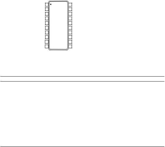
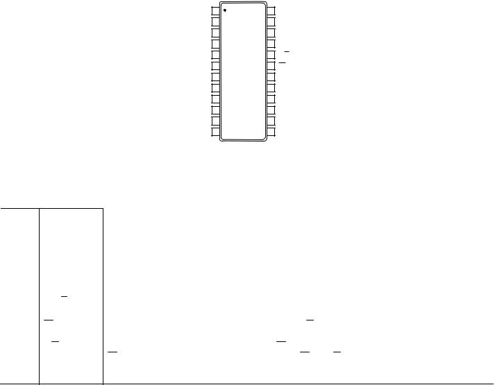
PIN CONFIGURATIONS AND FUNCTION DESCRIPTIONS
AGND |
1 |
|
20 |
IOUTB |
|
|||||||
I |
|
A |
2 |
|
19 |
R |
FB |
B |
|
|||
OUT |
|
|
|
|
|
|
|
|||||
R |
|
A |
3 |
|
18 |
V |
REF |
B |
|
|||
|
FB |
|
AD5428 |
|
|
|
|
|||||
VREFA |
4 |
|
VDD |
|
|
|||||||
TOP VIEW 17 |
|
|
||||||||||
|
|
|
|
(Not to Scale) |
|
|
|
|
|
|
|
|
DGND |
5 |
16 |
R/W |
|
|
|||||||
|
|
|
||||||||||
DAC |
|
|
6 |
|
15 |
|
|
|
|
|
||
A/B |
|
CS |
|
|
|
|
||||||
DB7 |
7 |
|
14 |
DB0 (LSB) |
||||||||
DB6 |
8 |
|
13 |
DB1 |
|
|
||||||
DB5 |
9 |
|
12 |
DB2 |
|
04462-004 |
||||||
DB4 10 |
|
11 |
DB3 |
|
||||||||
|
|
|
||||||||||
Figure 4. Pin Configuration 20-Lead TSSOP (RU-20)
Table 4. AD5428 Pin Function Descriptions
Pin No. |
|
Mnemonic |
Description |
|||||||||||
|
|
|
|
|
|
|
|
|
|
|
|
|
|
|
1 |
|
AGND |
DAC Ground Pin. This pin should typically be tied to the analog ground of the system, but can be biased to |
|||||||||||
|
|
|
|
|
|
|
|
achieve single-supply operation. |
||||||
2, 20 |
|
IOUTA, IOUTB |
DAC Current Outputs. |
|||||||||||
3, 19 |
|
RFBA, RFBB |
DAC Feedback Resistor Pins. These pins establish voltage output for the DAC by connecting to an external |
|||||||||||
|
|
|
|
|
|
|
|
amplifier output. |
||||||
4, 18 |
|
VREFA, VREFB |
DAC Reference Voltage Input Terminals. |
|||||||||||
5 |
|
DGND |
Digital Ground Pin. |
|||||||||||
6 |
|
|
|
|
|
|
|
Selects DAC A or DAC B. Low selects DAC A; high selects DAC B. |
||||||
|
DAC |
A/B |
||||||||||||
7 to14 |
DB7 to DB0 |
Parallel Data Bits 7 Through 0. |
||||||||||||
15 |
|
|
|
|
|
|
|
|
|
|
|
to load parallel data to the input latch or to read |
||
|
CS |
|
|
Chip Select Input. Active low. Used in conjunction with R/W |
||||||||||
|
|
|
|
|
|
|
|
data from the DAC register. |
||||||
16 |
|
|
|
|
Read/Write. When low, used in conjunction with |
|
to load parallel data. When high, used in conjunction |
|||||||
|
R/W |
|
CS |
|||||||||||
|
|
|
|
|
|
|
|
with |
CS |
to read back contents of the DAC register. |
||||
17 |
|
VDD |
Positive Power Supply Input. This part can be operated from a supply of 2.5 V to 5.5 V. |
|||||||||||
Rev. C | Page 7 of 32
AD5428/AD5440/AD5447 |
Data Sheet |
|
|
AGND |
1 |
|
24 |
IOUTB |
IOUTA |
2 |
|
23 |
RFBB |
RFBA |
3 |
|
22 |
VREFB |
VREFA |
4 |
AD5440 |
21 |
VDD |
|
|
|
|
DGND |
5 |
TOP VIEW 20 |
||
DAC |
|
|
6 |
(Not to Scale) |
A/B |
19 |
|||
DB9 |
7 |
18 |
||
DB8 |
8 |
17 |
||
DB7 |
9 |
16 |
||
DB6 10 |
15 |
|||
DB5 11 |
14 |
|||
DB4 12 |
13 |
|||
|
|
|
|
NC = NO CONNECT |
R/W
CS
NC
NC
DB0 (LSB)
DB1 |
|
|
DB2 |
04462-005 |
|
DB3 |
||
|
Figure 5. Pin Configuration 24-Lead TSSOP (RU-24)
Table 5. AD5440 Pin Function Descriptions
Pin No. |
Mnemonic |
1 |
AGND |
|
|
2, 24 |
IOUTA, IOUTB |
3, 23 |
RFBA, RFBB |
4, 22 |
VREFA, VREFB |
5DGND
6DAC A/B
7 to16 DB9 to DB0
19CS
20R/W
21VDD
Function
DAC Ground Pin. This pin should typically be tied to the analog ground of the system, but can be biased to achieve single-supply operation.
DAC Current Outputs.
DAC Feedback Resistor Pins. Establish voltage output for the DAC by connecting to an external amplifier output.
DAC Reference Voltage Input Terminals. Digital Ground Pin.
Selects DAC A or DAC B. Low selects DAC A; high selects DAC B. Parallel Data Bits 9 Through 0.
Chip Select Input. Active low. Used in conjunction with R/W to load parallel data to the input latch or to read data from the DAC register.
Read/Write. When low, used in conjunction with CS to load parallel data. When high, used in conjunction with CS to read back contents of the DAC register.
Positive Power Supply Input. This part can be operated from a supply of 2.5 V to 5.5 V.
Rev. C | Page 8 of 32
Data Sheet |
AD5428/AD5440/AD5447 |
|
|
AGND |
1 |
|
24 |
IOUTB |
IOUTA |
2 |
|
23 |
RFBB |
RFBA |
3 |
|
22 |
VREFB |
VREFA |
4 |
AD5447 |
21 |
VDD |
|
|
|
|
DGND |
5 |
TOP VIEW 20 |
||
DAC |
|
|
6 |
(Not to Scale) |
A/B |
19 |
|||
DB11 |
7 |
18 |
||
DB10 |
8 |
17 |
||
DB9 |
9 |
16 |
||
DB8 10 |
15 |
|||
DB7 11 |
14 |
|||
DB6 12 |
13 |
|||
R/W
CS
DB0 (LSB)
DB1 |
|
|
DB2 |
|
|
DB3 |
|
|
DB4 |
04462-006 |
|
DB5 |
||
|
Figure 6. Pin Configuration 24-Lead TSSOP (RU-24)
Table 6. AD5447 Pin Function Descriptions
Pin No. |
Mnemonic |
1 |
AGND |
2, 24 |
IOUTA, IOUTB |
3, 23 |
RFBA, RFBB |
4, 22 |
VREFA, VREFB |
5DGND
6DAC A/B
7 to 18 DB11 to DB0
19CS
20R/W
21VDD
Description
DAC Ground Pin. This pin should typically be tied to the analog ground of the system, but can be biased to achieve single-supply operation.
DAC Current Outputs.
DAC Feedback Resistor Pins. Establish voltage output for the DAC by connecting to an external amplifier output.
DAC Reference Voltage Input Terminals. Digital Ground Pin.
Selects DAC A or DAC B. Low selects DAC A; high selects DAC B. Parallel Data Bits 11 Through 0.
Chip Select Input. Active low. Used in conjunction with R/W to load parallel data to the input latch or to read data from the DAC register.
Read/Write. When low, used in conjunction with CS to load parallel data. When high, used in conjunction with
CS to read back the contents of the DAC register. When CS and R/W are held low, the latches are transparent. Any changes on the data lines are reflected in the relevant DAC output.
Positive Power Supply Input. This part can be operated from a supply of 2.5 V to 5.5 V.
Rev. C | Page 9 of 32

AD5428/AD5440/AD5447 |
Data Sheet |
|
|
TYPICAL PERFORMANCE CHARACTERISTICS
|
0.20 |
TA = 25°C |
|
0.20 |
TA = 25°C |
|
|
|
|
||
|
0.15 |
VREF = 10V |
|
0.15 |
VREF = 10V |
|
|
VDD = 5V |
|
|
VDD = 5V |
|
0.10 |
|
|
0.10 |
|
(LSB) |
0.05 |
|
(LSB) |
0.05 |
|
0 |
|
0 |
|
||
INL |
|
DNL |
|
||
–0.05 |
|
–0.05 |
|
||
|
|
|
|
||
|
–0.10 |
|
|
–0.10 |
|
|
–0.15 |
|
|
–0.15 |
|
|
–0.20 |
|
|
–0.20 |
|
0 |
50 |
100 |
150 |
200 |
250 |
0 |
50 |
100 |
150 |
200 |
250 |
|
|
|
CODE |
|
04462007- |
|
|
|
CODE |
|
|
|
Figure 7. INL vs. Code (8-Bit DAC) |
|
|
Figure 10. DNL vs. Code (8-Bit DAC) |
|
||||||
04462-010
|
0.5 |
|
|
|
|
|
|
0.4 |
TA = 25°C |
|
|
|
|
|
VREF = 10V |
|
|
|
|
|
|
|
|
|
|
|
|
|
0.3 |
VDD = 5V |
|
|
|
|
|
|
|
|
|
|
|
|
0.2 |
|
|
|
|
|
(LSB) |
0.1 |
|
|
|
|
|
0 |
|
|
|
|
|
|
INL |
–0.1 |
|
|
|
|
|
|
|
|
|
|
|
|
|
–0.2 |
|
|
|
|
|
|
–0.3 |
|
|
|
|
|
|
–0.4 |
|
|
|
|
|
|
–0.5 |
|
|
|
|
|
|
0 |
200 |
400 |
600 |
800 |
1000 |
|
|
|
|
CODE |
|
04462008- |
Figure 8. INL vs. Code (10-Bit DAC)
|
1.0 |
|
|
|
|
|
|
|
|
|
0.8 |
TA = 25°C |
|
|
|
|
|
|
|
|
|
VREF = 10V |
|
|
|
|
|
|
|
|
0.6 |
VDD = 5V |
|
|
|
|
|
|
|
|
|
|
|
|
|
|
|
|
|
|
0.4 |
|
|
|
|
|
|
|
|
(LSB) |
0.2 |
|
|
|
|
|
|
|
|
0 |
|
|
|
|
|
|
|
|
|
INL |
–0.2 |
|
|
|
|
|
|
|
|
|
|
|
|
|
|
|
|
|
|
|
–0.4 |
|
|
|
|
|
|
|
|
|
–0.6 |
|
|
|
|
|
|
|
|
|
–0.8 |
|
|
|
|
|
|
|
|
|
–1.0 |
500 |
1000 |
1500 |
2000 |
2500 |
3000 |
3500 |
4000 |
|
0 |
||||||||
|
|
|
|
|
CODE |
|
|
|
04462009- |
Figure 9. INL vs. Code (12-Bit DAC)
|
0.5 |
|
|
|
|
|
|
0.4 |
TA = 25°C |
|
|
|
|
|
VREF = 10V |
|
|
|
|
|
|
|
|
|
|
|
|
|
0.3 |
VDD = 5V |
|
|
|
|
|
|
|
|
|
|
|
|
0.2 |
|
|
|
|
|
(LSB) |
0.1 |
|
|
|
|
|
0 |
|
|
|
|
|
|
DNL |
|
|
|
|
|
|
–0.1 |
|
|
|
|
|
|
|
|
|
|
|
|
|
|
–0.2 |
|
|
|
|
|
|
–0.3 |
|
|
|
|
|
|
–0.4 |
|
|
|
|
|
|
–0.5 |
|
|
|
|
|
|
0 |
200 |
400 |
600 |
800 |
1000 |
|
|
|
|
CODE |
|
04462011- |
Figure 11. DNL vs. Code (10-Bit DAC)
|
1.0 |
|
|
|
|
|
|
|
|
|
0.8 |
TA = 25°C |
|
|
|
|
|
|
|
|
|
VREF = 10V |
|
|
|
|
|
|
|
|
0.6 |
VDD = 5V |
|
|
|
|
|
|
|
|
|
|
|
|
|
|
|
|
|
|
0.4 |
|
|
|
|
|
|
|
|
(LSB) |
0.2 |
|
|
|
|
|
|
|
|
0 |
|
|
|
|
|
|
|
|
|
DNL |
|
|
|
|
|
|
|
|
|
–0.2 |
|
|
|
|
|
|
|
|
|
|
|
|
|
|
|
|
|
|
|
|
–0.4 |
|
|
|
|
|
|
|
|
|
–0.6 |
|
|
|
|
|
|
|
|
|
–0.8 |
|
|
|
|
|
|
|
|
|
–1.0 |
500 |
1000 |
1500 |
2000 |
2500 |
3000 |
3500 |
4000 |
|
0 |
||||||||
|
|
|
|
|
CODE |
|
|
|
04462012- |
Figure 12. DNL vs. Code (12-Bit DAC)
Rev. C | Page 10 of 32
Loading...