


 Loading...
FEATURES
Low power, single nanoDACs AD5660: 16 bits
AD5640: 14 bits AD5620: 12 bits
12-bit accuracy guaranteed
On-chip, 1.25 V/2.5 V, 5 ppm/°C reference Tiny 8-lead SOT-23/MSOP packages Power-down to 480 nA @ 5 V, 200 nA @ 3 V 3 V/5 V single power supply
Guaranteed 16-bit monotonic by design Power-on reset to zero/midscale
3 power-down functions
Serial interface with Schmitt-triggered inputs Rail-to-rail operation
SYNC interrupt facility
Single, 12-/14-/16-Bit nanoDAC with 5 ppm/°C On-Chip Reference in SOT-23 AD5620/AD5640/AD5660
FUNCTIONAL BLOCK DIAGRAM
|
VREFOUT |
GND |
VDD |
|
|
POWER-ON |
1.25/2.5V |
AD5620/AD5640/AD5660 |
|
||
|
REF |
|
|
|
|
RESET |
|
|
|
VFB |
|
|
|
|
|
||
DAC |
REF(+) |
|
|
OUTPUT |
VOUT |
16-BIT |
|
BUFFER |
|||
REGISTER |
|
|
|||
DAC |
|
|
|
||
|
|
|
|
||
INPUT |
|
POWER-DOWN |
|
|
|
CONTROL |
|
RESISTOR |
|
||
CONTROL LOGIC |
|
||||
LOGIC |
NETWORK |
|
|||
|
|
|
|
||
|
|
|
|
|
04539-001 |
SYNC SCLK DIN
Figure 1.
APPLICATIONS
Process control
Data acquisition systems
Portable battery-powered instruments
Digital gain and offset adjustment
Programmable voltage and current sources
Programmable attenuators
PRODUCT HIGHLIGHTS
1.12-/14-/16-bit nanoDAC—12-bit accuracy guaranteed.
2.On-chip, 1.25 V/2.5 V, 5 ppm/°C reference.
3.Available in 8-lead SOT-23 and 8-lead MSOP packages.
4.Power-on reset to 0 V or midscale.
5.10 μs settling time.
Table 1. Related Device
Part No. |
Description |
|
|
AD5662 |
2.7 V to 5.5 V, 16-bit DAC in SOT-23, external |
|
reference |
GENERAL DESCRIPTION
The AD5620/AD5640/AD5660, members of the nanoDAC™ family of devices, are low power, single, 12-/14-/16-bit, buffered voltage-out DACs and are guaranteed monotonic by design.
The AD5620/AD5640/AD5660-1 parts include an internal, 1.25 V, 5 ppm/°C reference, giving a full-scale output voltage range of 2.5 V. The AD5620/AD5640/AD5660-2-3 parts include an internal, 2.5 V, 5 ppm/°C reference, giving a full-scale output voltage range of 5 V. The reference associated with each part is available at the VREFOUT pin.
The parts incorporate a power-on reset circuit to ensure that the DAC output powers up to 0 V (AD5620/AD5640/AD5660-1-2) or midscale (AD5620-3 and AD5660-3) and remains there until a valid write takes place. The parts contain a power-down feature that reduces the current consumption of the device to 480 nA at 5 V and provides software-selectable output loads while in power-down mode. The power consumption is
2.5 mW at 5 V, reducing to 1 μW in power-down mode.
The AD5620/AD5640/AD5660 on-chip precision output amplifier allows rail-to-rail output swing to be achieved. For remote sensing applications, the output amplifier’s inverting input is available to the user. The AD5620/AD5640/AD5660 use a versatile 3-wire serial interface that operates at clock rates up to 30 MHz and is compatible with standard SPI®, QSPI™, MICROWIRE™, and DSP interface standards.
Rev. F
Information furnished by Analog Devices is believed to be accurate and reliable. However, no responsibilityisassumedbyAnalogDevicesforitsuse,norforanyinfringementsofpatentsorother rightsofthirdpartiesthatmayresultfromitsuse.Specificationssubjecttochangewithoutnotice.No license is granted by implication or otherwise under any patent or patent rights of Analog Devices. Trademarksandregisteredtrademarksarethepropertyoftheirrespectiveowners.
One Technology Way, P.O. Box 9106, Norwood, MA 02062-9106, U.S.A. Tel: 781.329.4700 www.analog.com Fax: 781.461.3113 ©2005–2010 Analog Devices, Inc. All rights reserved.

AD5620/AD5640/AD5660
TABLE OF CONTENTS |
|
Features .............................................................................................. |
1 |
Applications....................................................................................... |
1 |
Product Highlights ........................................................................... |
1 |
Functional Block Diagram .............................................................. |
1 |
General Description ......................................................................... |
1 |
Revision History ............................................................................... |
2 |
Specifications..................................................................................... |
3 |
AD5620/AD5640/AD5660-2-3 .................................................. |
3 |
AD5620/AD5640/AD5660-1...................................................... |
5 |
Timing Characteristics ................................................................ |
7 |
Absolute Maximum Ratings............................................................ |
8 |
ESD Caution.................................................................................. |
8 |
Pin Configurations and Function Descriptions ........................... |
9 |
Typical Performance Characteristics ........................................... |
10 |
Terminology .................................................................................... |
16 |
Theory of Operation ...................................................................... |
17 |
D/A Section................................................................................. |
17 |
Resistor String............................................................................. |
17 |
REVISION HISTORY |
|
12/10—Rev. E to Rev. F |
|
Changes to Ordering Guide .......................................................... |
25 |
7/10—Rev. D to Rev. E |
|
Moved Using the AD5660 as an Isolated, Programmable, 4 mA |
|
to 20 mA Process Controller Section........................................... |
22 |
Moved Power Supply Bypassing and Grounding Section......... |
23 |
Changes to Ordering Guide .......................................................... |
25 |
3/10—Rev. C to Rev. D |
|
Changes to Ordering Guide .......................................................... |
24 |
10/09—Rev. B to Rev. C |
|
Changes to Ordering Guide .......................................................... |
23 |
Internal Reference ...................................................................... |
17 |
Output Amplifier........................................................................ |
17 |
Serial Interface ............................................................................ |
17 |
Input Shift Register .................................................................... |
18 |
SYNC Interrupt .......................................................................... |
18 |
Power-On Reset.......................................................................... |
19 |
Power-Down Modes .................................................................. |
19 |
Microprocessor Interfacing....................................................... |
19 |
Applications Information .............................................................. |
21 |
Using a REF19x as a Power Supply for the |
|
AD5620/AD5640/AD5660 ....................................................... |
21 |
Bipolar Operation Using the AD5660 ..................................... |
21 |
Using the AD5660 as an Isolated, Programmable, 4 mA to |
|
20 mA Process Controller ......................................................... |
22 |
Using the AD5620/AD5640/AD5660 with a Galvanically |
|
Isolated Interface ........................................................................ |
22 |
Power Supply Bypassing and Grounding................................ |
23 |
Outline Dimensions ....................................................................... |
24 |
Ordering Guide .......................................................................... |
25 |
5/06—Rev. A to Rev. B |
|
Updated Formatted ............................................................ |
Universal |
Updated Temperature Range ............................................ |
Universal |
Changes to Table 2............................................................................. |
3 |
Changes to Table 5............................................................................. |
8 |
Replaced Figure 17, Figure 18, and Figure 19............................. |
12 |
Changes to Ordering Guides .................................................. |
23, 24 |
9/05—Rev. 0 to Rev. A |
|
Changes to Specifications................................................................. |
5 |
Changes to Outline Dimensions .................................................. |
23 |
7/05—Revision 0: Initial Version |
|
Rev. F | Page 2 of 28

AD5620/AD5640/AD5660
SPECIFICATIONS
AD5620/AD5640/AD5660-2-3
VDD = 4.5 V to 5.5 V, RL = 2 kΩ to GND, CL = 200 pF to GND, CREFOUT = 100 nF; all specifications TMIN to TMAX, unless otherwise noted.
Table 2.
Parameter |
A Grade1 |
B Grade1 |
C Grade1 |
Unit |
Conditions/Comments |
STATIC PERFORMANCE2 |
|
|
|
|
|
AD5660 |
|
|
|
|
|
Resolution |
16 |
16 |
16 |
Bits min |
|
Relative Accuracy |
±32 |
±16 |
±16 |
LSB max |
|
Differential Nonlinearity |
±1 |
±1 |
±1 |
LSB max |
Guaranteed monotonic by design |
AD5640 |
|
|
|
|
|
Resolution |
14 |
14 |
14 |
Bits min |
|
Relative Accuracy |
±8 |
±4 |
±4 |
LSB max |
|
Differential Nonlinearity |
±0.5 |
±0.5 |
±0.5 |
LSB max |
Guaranteed monotonic by design |
AD5620 |
|
|
|
|
|
Resolution |
12 |
12 |
12 |
Bits min |
|
Relative Accuracy |
±6 |
±1 |
±1 |
LSB max |
|
Differential Nonlinearity |
±0.25 |
±0.25 |
±0.25 |
LSB max |
Guaranteed monotonic by design |
Zero-Code Error |
2 |
2 |
2 |
mV typ |
All 0s loaded to DAC register |
|
10 |
10 |
10 |
mV max |
|
Offset Error |
±10 |
±10 |
±10 |
mV max |
|
Full-Scale Error |
−0.15 |
−0.15 |
−0.15 |
% FSR typ |
All 1s loaded to DAC register |
|
±1 |
±1 |
±1 |
% FSR max |
|
Gain Error |
±1.5 |
±1.5 |
±1.5 |
% FSR max |
|
Zero-Code Error Drift |
±2 |
±2 |
±2 |
μV/°C typ |
|
Gain Temperature Coefficient |
±2.5 |
±2.5 |
±2.5 |
ppm typ |
Of FSR/°C |
DC Power Supply Rejection Ratio |
−75 |
−75 |
−75 |
dB typ |
DAC code = midscale; VDD = 5 V ± 10% |
|
|
|
|
|
|
OUTPUT CHARACTERISTICS3 |
|
|
|
|
|
Output Voltage Range |
0 |
0 |
0 |
V min |
|
|
VDD |
VDD |
VDD |
V max |
|
Output Voltage Settling Time |
8 |
8 |
8 |
μs typ |
¼ to ¾ scale change settling to ±2 LSB |
|
10 |
10 |
10 |
μs max |
RL = 2 kΩ; 0 pF < CL < 200 pF |
Slew Rate |
1.5 |
1.5 |
1.5 |
V/μs typ |
¼ to ¾ scale |
Capacitive Load Stability |
2 |
2 |
2 |
nF typ |
RL = ∞ |
|
10 |
10 |
10 |
nF typ |
RL = 2 kΩ |
Output Noise Spectral Density |
80 |
80 |
80 |
nV/√Hz typ |
DAC code = midscale, 10 kHz |
Output Noise (0.1 Hz to 10 Hz) |
45 |
45 |
45 |
μV p-p typ |
DAC code = midscale |
Digital-to-Analog Glitch Impulse |
5 |
5 |
5 |
nV-s typ |
1 LSB change around major carry |
Digital Feedthrough |
0.1 |
0.1 |
0.1 |
nV-s typ |
|
DC Output Impedance |
0.5 |
0.5 |
0.5 |
Ω typ |
|
Short-Circuit Current |
30 |
30 |
30 |
mA typ |
VDD = 5 V |
Power-Up Time |
5 |
5 |
5 |
μs typ |
Coming out of power-down mode; VDD = 5 V |
REFERENCE OUTPUT |
|
|
|
|
|
Output Voltage |
2.495 |
2.495 |
2.495 |
V min |
At ambient |
|
2.505 |
2.505 |
2.505 |
V max |
|
Reference TC3 |
±10 |
±10 |
±5 |
ppm/°C typ |
|
|
|
|
±10 |
ppm/°C max |
|
Output Impedance |
7.5 |
7.5 |
7.5 |
kΩ typ |
|
Rev. F | Page 3 of 28

AD5620/AD5640/AD5660
Parameter |
A Grade1 |
B Grade1 |
C Grade1 |
Unit |
Conditions/Comments |
LOGIC INPUTS3 |
|
|
|
|
|
Input Current |
±2 |
±2 |
±2 |
μA max |
All digital inputs |
VINL, Input Low Voltage |
0.8 |
0.8 |
0.8 |
V max |
VDD = 5 V |
VINH, Input High Voltage |
2 |
2 |
2 |
V min |
VDD = 5 V |
Pin Capacitance |
3 |
3 |
3 |
pF typ |
|
POWER REQUIREMENTS |
|
|
|
|
|
VDD |
4.5 |
4.5 |
4.5 |
V min |
All digital inputs at 0 V or VDD |
|
5.5 |
5.5 |
5.5 |
V max |
DAC active and excluding load current |
IDD (Normal Mode) |
|
|
|
|
|
VDD = 4.5 V to 5.5 V |
0.55 |
0.55 |
0.55 |
mA typ |
VIH = VDD and VIL = GND |
VDD = 4.5 V to 5.5 V |
1 |
1 |
1 |
mA max |
VIH = VDD and VIL = GND |
IDD (All Power-Down Modes) |
|
|
|
|
|
VDD = 4.5 V to 5.5 V |
0.48 |
0.48 |
0.48 |
μA typ |
VIH = VDD and VIL = GND |
VDD = 4.5 V to 5.5 V |
1 |
1 |
1 |
μA max |
VIH = VDD and VIL = GND |
|
|
|
|
|
|
1 Temperature range is −40°C to +105°C, typical at +25°C.
2Linearity calculated using a reduced code range: AD5660 (Code 511 to Code 65024); AD5640 (Code 128 to Code 16256); AD5620 (Code 32 to Code 4064). Output unloaded. Linearity tested with VDD = 5.5 V. If part is operated with a VDD < 5 V, the output is clamped to VDD.
3 Guaranteed by design and characterization; not production tested.
Rev. F | Page 4 of 28

AD5620/AD5640/AD5660
AD5620/AD5640/AD5660-1
VDD1 = 2.7 V to 3.3 V, RL = 2 kΩ to GND, CL = 200 pF to GND, CREFOUT = 100 nF; all specifications TMIN to TMAX, unless otherwise noted.
Table 3.
Parameter |
A Grade2 |
B Grade2 |
C Grade2 |
Unit |
Conditions/Comments |
STATIC PERFORMANCE3 |
|
|
|
|
|
AD5660 |
|
|
|
|
|
Resolution |
16 |
16 |
16 |
Bits min |
|
Relative Accuracy |
±32 |
±16 |
±16 |
LSB max |
|
Differential Nonlinearity |
±1 |
±1 |
±1 |
LSB max |
Guaranteed monotonic by design |
AD5640 |
|
|
|
|
|
Resolution |
14 |
14 |
14 |
Bits min |
|
Relative Accuracy |
±8 |
±4 |
±4 |
LSB max |
|
Differential Nonlinearity |
±0.5 |
±0.5 |
±0.5 |
LSB max |
Guaranteed monotonic by design |
AD5620 |
|
|
|
|
|
Resolution |
12 |
12 |
12 |
Bits min |
|
Relative Accuracy |
±6 |
±1 |
±1 |
LSB max |
|
Differential Nonlinearity |
±0.25 |
±0.25 |
±0.25 |
LSB max |
Guaranteed monotonic by design |
Zero-Code Error |
2 |
2 |
2 |
mV typ |
All 0s loaded to DAC register |
|
8 |
8 |
8 |
mV max |
|
Offset Error |
±9 |
±9 |
±9 |
mV max |
|
Full-Scale Error |
±0.15 |
±0.15 |
±0.15 |
% FSR typ |
All 1s loaded to DAC register |
|
±0.85 |
±0.85 |
±0.85 |
% FSR max |
|
Gain Error |
±0.85 |
±0.85 |
±0.85 |
% FSR max |
|
Zero-Code Error Drift |
±2 |
±2 |
±2 |
μV/°C typ |
|
Gain Temperature Coefficient |
±2.5 |
±2.5 |
±2.5 |
ppm typ |
Of FSR/°C |
DC Power Supply Rejection Ratio |
−60 |
−60 |
−60 |
dB typ |
DAC code = midscale; VDD = 3 V ± 10% |
|
|
|
|
|
|
OUTPUT CHARACTERISTICS4 |
|
|
|
|
|
Output Voltage Range |
0 |
0 |
|
V min |
|
|
VDD |
VDD |
VDD |
V max |
|
Output Voltage Settling Time |
8 |
8 |
8 |
μs typ |
¼ to ¾ scale change settling to ±2 LSB |
|
10 |
10 |
10 |
μs max |
RL = 2 kΩ; 0 pF < CL < 200 pF |
Slew Rate |
1.5 |
1.5 |
1.5 |
V/μs typ |
¼ to ¾ scale |
Capacitive Load Stability |
2 |
2 |
2 |
nF typ |
RL = ∞ |
|
10 |
10 |
10 |
nF typ |
RL = 2 kΩ |
Output Noise Spectral Density |
80 |
80 |
80 |
nV/√Hz typ |
DAC code = midscale, 10 kHz |
Output Noise (0.1 Hz to 10 Hz) |
20 |
20 |
20 |
μV p-p typ |
DAC code = midscale |
Digital-to-Analog Glitch Impulse |
5 |
5 |
5 |
nV-s typ |
1 LSB change around major carry |
Digital Feedthrough |
0.1 |
0.1 |
0.1 |
nV-s typ |
|
DC Output Impedance |
0.5 |
0.5 |
0.5 |
Ω typ |
|
Short-Circuit Current |
30 |
30 |
30 |
mA typ |
VDD = 3 V |
Power-Up Time |
6 |
6 |
6 |
μs typ |
Coming out of power-down mode; VDD = 3 V |
|
|
|
|
|
|
REFERENCE OUTPUT |
|
|
|
|
|
Output Voltage |
1.247 |
1.247 |
1.247 |
V min |
At ambient |
|
1.253 |
1.253 |
1.253 |
V max |
|
Reference TC4 |
±10 |
±10 |
±5 |
ppm/°C typ |
|
|
|
|
±15 |
ppm/°C max |
|
Output Impedance |
7.5 |
7.5 |
7.5 |
kΩ typ |
|
Rev. F | Page 5 of 28

AD5620/AD5640/AD5660
Parameter |
A Grade2 |
B Grade2 |
C Grade2 |
Unit |
Conditions/Comments |
LOGIC INPUTS4 |
|
|
|
|
|
Input Current |
±1 |
±1 |
±1 |
μA max |
All digital inputs |
VINL, Input Low Voltage |
0.8 |
0.8 |
0.8 |
V max |
VDD = 3 V |
VINH, Input High Voltage |
2 |
2 |
2 |
V min |
VDD = 3 V |
Pin Capacitance |
3 |
3 |
3 |
pF max |
|
POWER REQUIREMENTS |
|
|
|
|
|
VDD |
2.7 |
2.7 |
2.7 |
V min |
All digital inputs at 0 V or VDD |
|
3.3 |
3.3 |
3.3 |
V max |
DAC active and excluding load current |
IDD (Normal Mode) |
|
|
|
|
|
VDD = 2.7 V to 3.3 V |
0.55 |
0.55 |
0.55 |
mA typ |
VIH = VDD and VIL = GND |
VDD = 2.7 V to 3.3 V |
0.65 |
0.65 |
0.65 |
mA max |
VIH = VDD and VIL = GND |
IDD (All Power-Down Modes) |
|
|
|
|
|
VDD = 2.7 V to 3.3 V |
0.2 |
0.2 |
0.2 |
μA typ |
VIH = VDD and VIL = GND |
VDD = 2.7 V to 3.3 V |
0.25 |
0.25 |
0.25 |
μA max |
VIH = VDD and VIL = GND |
|
|
|
|
|
|
1 Part is functional with VDD up to 5.5 V.
2 Temperature range is −40°C to +105°C, typical at +25°C.
3 Linearity calculated using a reduced code range: AD5660 (Code 511 to Code 65024); AD5640 (Code 128 to Code 16256); AD5620 (Code 32 to Code 4064). Output unloaded.
4 Guaranteed by design and characterization; not production tested.
Rev. F | Page 6 of 28

AD5620/AD5640/AD5660
TIMING CHARACTERISTICS
All input signals are specified with tr = tf = 1 ns/V (10% to 90% of VDD) and timed from a voltage level of (VIL + VIH)/2. See Figure 2. VDD = 2.7 V to 5.5 V; all specifications TMIN to TMAX, unless otherwise noted.
Table 4.
|
Limit at TMIN, TMAX |
|
|
|
|
|
|
|
|
|
Parameter |
VDD = 2.7 V to 3.6 V |
VDD = 3.6 V to 5.5 V |
Unit |
|
Conditions/Comments |
|||||
t11 |
50 |
33 |
ns min |
|
SCLK cycle time |
|||||
t2 |
13 |
13 |
ns min |
|
SCLK high time |
|||||
t3 |
13 |
13 |
ns min |
|
SCLK low time |
|||||
t4 |
13 |
13 |
ns min |
|
|
|
|
|
|
|
|
SYNC |
to SCLK falling edge setup time |
||||||||
t5 |
5 |
5 |
ns min |
|
Data setup time |
|||||
t6 |
4.5 |
4.5 |
ns min |
|
Data hold time |
|||||
t7 |
0 |
0 |
ns min |
|
|
|
|
|||
|
SCLK falling edge to |
SYNC |
rising edge |
|||||||
t8 |
50 |
33 |
ns min |
|
|
|||||
|
Minimum |
SYNC |
high time |
|||||||
t9 |
13 |
13 |
ns min |
|
|
|||||
|
SYNC |
rising edge to SCLK fall ignore |
||||||||
t10 |
0 |
0 |
ns min |
|
|
|||||
|
SCLK falling edge to |
SYNC |
fall ignore |
|||||||
|
|
|
|
|
|
|
|
|
|
|
1 Maximum SCLK frequency is 30 MHz at VDD = 3.6 V to 5.5 V and 20 MHz at VDD = 2.7 V to 3.6 V.
|
|
t10 |
|
t1 |
|
t9 |
|
|
|
|
|
|
|
SCLK |
|
|
|
|
|
|
|
t8 |
t4 |
t3 |
|
t2 |
t7 |
|
|
|
|
|||
SYNC |
|
|
|
|
|
|
|
|
|
t6 |
|
|
|
|
|
|
t5 |
|
|
|
DIN |
|
MSB |
|
|
|
LSB |
LSB = DB0
MSB = DB23 FOR AD5660
MSB = DB15 FOR AD5620/AD5640
Figure 2. Serial Write Operation
04539-002
Rev. F | Page 7 of 28

AD5620/AD5640/AD5660
ABSOLUTE MAXIMUM RATINGS
TA = 25°C, unless otherwise noted.
Table 5.
Parameter |
Rating |
VDD to GND |
−0.3 V to +7 V |
VOUT to GND |
−0.3 V to VDD + 0.3 V |
VFB to GND |
−0.3 V to VDD + 0.3 V |
VREFOUT to GND |
−0.3 V to VDD + 0.3 V |
Digital Input Voltage to GND |
−0.3 V to VDD + 0.3 V |
Operating Temperature Range |
|
Industrial |
−40°C to +105°C |
Storage Temperature Range |
−65°C to +150°C |
Junction Temperature (TJ max) |
150°C |
Power Dissipation |
(TJ max − TA)/θJA |
SOT-23 Package (4-Layer Board) |
|
θJA Thermal Impedance |
119°C/W |
MSOP Package (4-Layer Board) |
|
θJA Thermal Impedance |
141°C/W |
θJC Thermal Impedance |
44°C/W |
Reflow Soldering Peak Temperature |
|
SnPb |
240°C |
Pb-Free |
260°C |
Stresses above those listed under Absolute Maximum Ratings may cause permanent damage to the device. This is a stress rating only; functional operation of the device at these or any other conditions above those indicated in the operational section of this specification is not implied. Exposure to absolute maximum rating conditions for extended periods may affect device reliability.
ESD CAUTION
Rev. F | Page 8 of 28
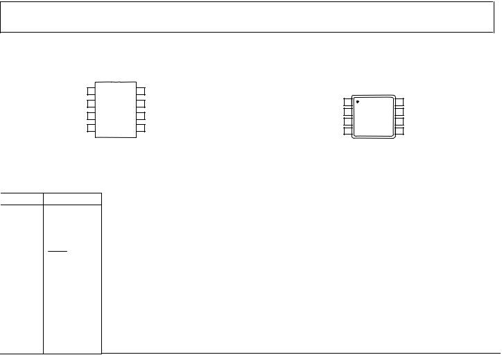
PIN CONFIGURATIONS AND FUNCTION DESCRIPTIONS
VDD |
1 |
AD5620/ |
8 |
GND |
|
||
V |
2 |
AD5640/ |
7 |
DIN |
|
||
REFOUT |
|
AD5660 |
|
|
|
|
|
VFB |
3 |
6 |
SCLK |
|
|||
TOP VIEW |
003-04539 |
||||||
VOUT |
4 |
(Not to Scale) |
5 |
|
|
|
|
|
SYNC |
|
|
||||
Figure 3. SOT-23 Pin Configuration
AD5620/AD5640/AD5660
VDD |
1 |
AD5620/ |
8 |
GND |
|
||
VREFOUT |
2 |
AD5640/ |
7 |
DIN |
|
||
VFB |
3 |
AD5660 |
6 |
SCLK |
-04539004 |
||
|
|
TOP VIEW |
|
|
|
|
|
VOUT |
4 |
(Not to Scale) |
5 |
SYNC |
|
||
Figure 4. MSOP Pin Configuration
Table 6. Pin Function Descriptions
Pin No. Mnemonic
1VDD
2VREFOUT
3VFB
4VOUT
5SYNC
6SCLK
7DIN
8GND
Description
Power Supply Input. These parts can operate from 2.7 V to 5.5 V. VDD should be decoupled to GND. Reference Voltage Output.
Feedback Connection for the Output Amplifier. VFB should be connected to VOUT for normal operation. Analog Output Voltage from DAC. The output amplifier has rail-to-rail operation.
Level-Triggered Control Input (Active Low). This is the frame synchronization signal for the input data. When SYNC goes low, it enables the input shift register and data is transferred in on the falling edges of the following clocks. The DAC is updated following the 24th clock cycle for the AD5660 and the 16th clock cycle for AD5620/AD5640 unless SYNC is taken high before this edge. In this case, the rising edge of SYNC acts as an interrupt, and the write sequence is ignored by the DAC.
Serial Clock Input. Data is clocked into the input shift register on the falling edge of the serial clock input. Data can be transferred at rates up to 30 MHz.
Serial Data Input. The AD5660 has a 24-bit shift register, and the AD5620/AD5640 have a 16-bit shift register. Data is clocked into the register on the falling edge of the serial clock input.
Ground Reference Point for all Circuitry on the Part.
Rev. F | Page 9 of 28
Loading...