


|
|
|
Single Channel, 12-Bit, Serial Input, |
|||
|
|
|
Current Source & Voltage Output DAC |
|||
Preliminary Technical Data |
|
|
AD5412 |
|
||
|
|
|
|
|
|
|
FEATURES |
|
GENERAL DESCRIPTION |
|
|
||
12-Bit Resolution and Monotonicity |
|
The AD5412 is a low-cost, precision, fully integrated 12-bit |
||||
Current Output Ranges: 4–20mA, 0–20mA or 0–24mA |
|
converter offering a programmable current source and |
||||
0.1% Total Unadjusted Error (TUE) |
|
programmable voltage output designed to meet the |
||||
5ppm/°C Output Drift |
|
requirements of industrial process control applications. |
||||
|
The output current range is programmable to 4mA to 20 mA, |
|||||
Voltage Output Ranges: 0-5V, 0-10V, ±5V, ±10V, |
|
|||||
|
0mA to 20mA or an overrange function of 0mA to 24mA. |
|||||
10% over-range |
|
|||||
|
Voltage output is provided from a separate pin that can be |
|||||
0.05% Total Unadjusted Error (TUE) |
|
|||||
|
configured to provide 0V to 5V, 0V to 10V, ±5V or ±10V |
|||||
3ppm/°C Output Drift |
|
|||||
|
output ranges, an over-range of 10% is available on all ranges. |
|||||
Flexible Serial Digital Interface |
|
Analog outputs are short and open circuit protected and can |
||||
On-Chip Output Fault Detection |
|
drive capacitive loads of 1uF and inductive loads of 1H. |
||||
On-Chip Reference (10 ppm/°C Max) |
|
The device is specified to operate with a power supply range |
||||
Asynchronous CLEAR Function |
|
from 10.8 V to 40 V. Output loop compliance is 0 V to AVDD – |
||||
Power Supply Range |
|
2.5 V. |
|
|
||
AVDD : 10.8V to 40 V |
|
The flexible serial interface is SPI and MICROWIRE |
||||
AVSS : -26.4V to -3V/0V |
|
compatible and can be operated in 3-wire mode to minimize the |
||||
|
digital isolation required in isolated applications. |
|||||
Output Loop Compliance to AVDD – 2.5 V |
|
|||||
|
The device also includes a power-on-reset function ensuring |
|||||
Temperature Range: -40°C to +85°C |
|
|||||
|
that the device powers up in a known state and an |
|||||
TSSOP and LFCSP Packages |
|
|||||
|
asynchronous CLEAR pin which sets the outputs to zero-scale / |
|||||
PLC |
|
|
|
midale voltage output or the low end of the selected current |
||
MacshbM |
||||||
APPLICATIONS |
|
r nge. |
|
|
||
Process Control |
|
The total output error is typically ±0.1% in current mode and |
||||
Actuator Control |
|
±0.05% in voltage mode. |
|
|
||
|
|
|
|
|
|
|
|
|
|
|
Table 1. Related Devices |
|
|
|
|
|
|
Part Number |
Description |
|
|
|
|
|
|
|
|
|
|
|
|
AD5422 |
Single Channel, 16-Bit, Serial |
|
|
|
|
|
|
Input Current Source and |
|
|
|
|
|
|
Voltage Output DAC |
|
|
|
|
|
AD5420 |
Single Channel, 16-Bit, Serial |
|
|
|
|
|
|
Input Current Source DAC |
|
|
|
|
|
AD5410 |
Single Channel, 12-Bit, Serial |
|
|
|
|
|
|
Input Current Source DAC |
|
Rev. PrC
Information furnished by Analog Devices is believed to be accurate and reliable. However, no responsibilityisassumedbyAnalogDevicesforitsuse,norforanyinfringementsofpatentsorother rightsofthirdpartiesthatmayresultfromitsuse.Specificationssubjecttochangewithoutnotice.No license is granted by implication or otherwise under any patent or patent rights of Analog Devices. Trademarksandregisteredtrademarksarethepropertyoftheirrespectiveowners.
One Technology Way, P.O. Box 9106, Norwood, MA 02062-9106, U.S.A.
Tel: 781.329.4700 |
www.analog.com |
Fax: 781.461.3113 |
©2007 Analog Devices, Inc. All rights reserved. |

AD5412 |
|
|
Preliminary Technical Data |
|
|
|
|
|
|
|
|
TABLE OF CONTENTS |
|
|
|
|
|
Features .............................................................................................. |
1 |
RESET register............................................................................ |
29 |
|
|
Applications....................................................................................... |
1 |
Status register.............................................................................. |
30 |
|
|
General Description ......................................................................... |
1 |
Features ............................................................................................ |
31 |
|
|
Revision History ............................................................................... |
2 |
fault alert...................................................................................... |
31 |
|
|
Functional Block Diagram .............................................................. |
3 |
voltage output short circuit protection.................................... |
31 |
|
|
Specifications..................................................................................... |
4 |
Asynchronous Clear (CLEAR) ................................................. |
31 |
|
|
AC Performance Characteristics ................................................ |
7 |
Internal Reference ...................................................................... |
31 |
|
|
Timing Characteristics ................................................................ |
8 |
External current setting resistor............................................... |
31 |
|
|
Absolute Maximum Ratings.......................................................... |
10 |
Voltage ouTput over-range........................................................ |
31 |
|
|
ESD Caution................................................................................ |
10 |
Digital Power Supply.................................................................. |
31 |
|
|
Pin Configuration and Function Descriptions........................... |
11 |
External boost function............................................................. |
31 |
|
|
Typical Performance Characteristics Voltage output............... |
13 |
digital Slew rate control............................................................. |
32 |
|
|
Typical Performance Characteristics current output ............... |
17 |
IOUT Filtering Capacitors............................................................ |
32 |
|
|
Typical Performance Characteristics general ............................ |
20 |
Applications Information .............................................................. |
33 |
|
|
Terminology .................................................................................... |
22 |
driving inductive loads .............................................................. |
33 |
|
|
Theory of Operation ...................................................................... |
24 |
Transient voltage protection ..................................................... |
33 |
|
|
Architecture................................................................................. |
24 |
Layout Guidelines....................................................................... |
33 |
|
|
Serial Interface ............................................................................ |
24 |
G lvani ally Isolated Interface ................................................. |
33 |
|
|
Default configuration................................................................. |
28 |
Micropro essor Interfacing....................................................... |
33 |
|
|
....................................................................... |
|
Thermal and supply con iderations......................................... |
34 |
|
|
Transfer Function MacshbM28 |
|||||
Data Register ............................................................................... |
29 |
Outline Dimensions ....................................................................... |
35 |
|
|
Control Register.......................................................................... |
29 |
Ordering Guide .......................................................................... |
35 |
|
|
REVISION HISTORY
PrC – Preliminary Version. October 9, 2007
Rev. PrC | Page 2 of 37
Preliminary Technical Data |
AD5412 |
|
|
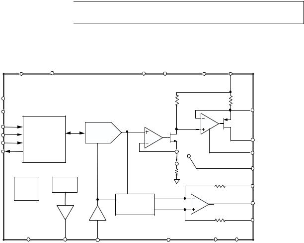
FUNCTIONAL BLOCK DIAGRAM
|
DVCC |
DVCC |
|
CAP1 |
CAP2 |
AVSS |
AVDD |
|
|
SELECT |
|
||||||
CLEAR |
AD5412 |
|
|
R2 |
|
|
|
|
|
|
|
|
|
|
R3 |
||
SELECT |
|
|
|
|
|
|
||
CLEAR |
|
|
|
|
|
|
|
BOOST |
LATCH |
INPUT SHIFT |
12 |
12-BIT |
|
|
|
|
|
SCLK |
REGISTER |
|
|
|
|
|||
/ |
DAC |
|
|
|
IOUT |
|||
SDIN |
AND |
|
|
|
|
|
||
CONTROL |
|
|
|
|
|
|
||
SDO |
|
|
|
|
|
|
||
LOGIC |
|
|
|
|
|
FAULT |
||
|
|
|
|
|
R1 |
|
|
RSET |
|
|
|
|
|
|
|
|
|
|
POWER |
VREF |
|
|
|
|
|
+VSENSE |
|
ON |
|
|
|
|
|
||
|
|
|
|
|
|
|
|
|
|
RESET |
|
|
RANGE |
|
|
|
|
|
|
|
|
|
|
|
VOUT |
|
|
|
|
|
SCALING |
|
|
|
|
|
|
|
|
|
|
|
|
|
|
|
|
|
|
|
|
|
-VSENSE |
|
DGND* |
REFOUT |
REFIN |
AGND |
CCOMP2 |
CCOMP1 |
||
MacshbM |
||||||||
*LFCSP Package
Figure 1.
Rev. PrC | Page 3 of 37

AD5412 |
Preliminary Technical Data |
|
|
SPECIFICATIONS
AVDD = 10.8V to 40V, AVSS = -26.4V to -3V/0V, AVDD + |AVSS| < 52.8V, AGND = DGND = 0 V, REFIN= +5 V external; DVCC = 2.7 V to 5.5 V, VOUT : RL = 2 kΩ, CL = 200 pF, IOUT : RL = 300Ω, HL = 50mH;
all specifications TMIN to TMAX, ±10 V / 0 to 24 mA range unless otherwise noted.
Table 2.
Parameter |
|
Value1 |
|
Unit |
Test Conditions/Comments |
VOLTAGE OUTPUT |
|
|
|
|
|
Output Voltage Ranges |
0 to 5 |
|
V |
|
|
|
|
0 to 10 |
|
V |
|
|
|
-5 to +5 |
|
V |
|
|
|
-10 to +10 |
|
V |
|
ACCURACY |
|
|
|
|
Output unloaded |
Bipolar Output |
|
|
|
|
|
Resolution |
12 |
|
Bits |
|
|
Total Unadjusted Error (TUE) |
0.1 |
|
% FSR max |
Over temperature, supplies, and time, typically 0.05% |
|
|
|
|
|
|
FSR |
TUE TC2 |
|
±3 |
|
ppm typ |
|
Relative Accuracy (INL) |
±0.012 |
|
% FSR max |
|
|
Differential Nonlinearity (DNL) |
±1 |
|
LSB max |
Guaranteed monotonic |
|
Bipolar Zero Error |
±5 |
|
mV max |
@ 25°C, error at other temperatures obtained using |
|
|
|
|
|
|
bipolar zero TC |
Bipolar Zero TC2 |
±3 |
|
ppm FSR/°C max |
|
|
Zero-Scale Error |
±1 |
|
mV max |
@ 25°C, error at other temperatures obtained using zero |
|
|
|
|
|
MacshbM |
|
|
|
|
TC |
||
Zero-Scale TC2 |
±3 |
|
ppm FSR/°C m x |
ale TC |
|
Gain Error |
|
±0.05 |
|
% FSR max |
@ 25°C, error at other temperatures obtained using gain |
Gain TC2 |
|
±8 |
|
ppm FSR/°C max |
|
Full-Scale Error |
0.05 |
|
% FSR max |
@ 25°C, error at other temperatures obtained using gain |
|
|
|
|
|
|
TC |
Full-Scale TC2 |
±3 |
|
ppm FSR/°C max |
|
|
Unipolar Output |
|
|
|
AVSS = 0 V |
|
Resolution |
12 |
|
Bits |
|
|
Total Unadjusted Error (TUE) |
0.1 |
|
% FSR max |
Over temperature, supplies, and time, typically 0.05% |
|
|
|
|
|
|
FSR |
Relative Accuracy (INL) |
±0.012 |
|
% FSR max |
|
|
Differential Nonlinearity (DNL) |
±1 |
|
LSB max |
Guaranteed monotonic |
|
Zero Scale Error |
+10 |
|
mV max |
@ 25°C, error at other temperatures obtained using gain |
|
|
|
|
|
|
TC |
Zero Scale TC2 |
±3 |
|
ppm FSR/°C max |
|
|
Offset Error |
±10 |
|
mV max |
|
|
Gain Error |
|
±0.05 |
|
% FSR max |
@ 25°C, error at other temperatures obtained using gain |
|
|
|
|
|
TC |
Gain TC2 |
|
±3 |
|
ppm FSR/°C max |
|
Full-Scale Error |
0.05 |
|
% FSR max |
@ 25°C, error at other temperatures obtained using gain |
|
|
|
|
|
|
TC |
Full-Scale TC2 |
±3 |
|
ppm FSR/°C max |
|
|
OUTPUT CHARACTERISTICS2 |
|
|
|
|
|
Headroom |
|
0.8 |
|
V max |
|
|
|
0.5 |
|
V typ |
|
Output Voltage TC |
±3 |
|
ppm FSR/°C max |
|
|
Output Voltage Drift vs. Time |
±12 |
|
ppm FSR/500 hr typ |
Vout = ¾ of Full-Scale |
|
|
|
±15 |
|
ppm FSR/1000 hr typ |
|
Short-Circuit Current |
12 |
|
mA typ |
|
|
|
|
|
|
|
|
Rev. PrC | Page 4 of 37

Preliminary Technical Data |
|
|
|
AD5412 |
|
||
|
|
|
|
|
|
|
|
|
|
|
|
|
|
|
|
Parameter |
|
Value1 |
|
Unit |
Test Conditions/Comments |
||
Load |
|
2 |
|
|
kΩ min |
For specified performance |
|
Capacitive Load Stability |
|
|
|
|
|
|
|
RL = ∞ |
|
20 |
|
|
nF max |
|
|
RL = 2 kΩ |
|
TBD |
|
nF max |
|
|
|
RL = ∞ |
|
1 |
|
|
µF max |
External compensation capacitor of 4nF connected. |
|
DC Output Impedance |
0.3 |
|
|
Ω typ |
|
|
|
Power-On Time |
|
10 |
|
|
µs typ |
|
|
DC PSRR |
|
TBD |
|
µV/V |
|
|
|
|
|
|
|
|
|
|
|
CURRENT OUTPUT |
|
|
|
|
|
|
|
Output Current Ranges |
0 to 24 |
|
mA |
|
|
||
|
|
0 to 20 |
|
mA |
|
|
|
|
|
4 to 20 |
|
mA |
|
|
|
ACCURACY |
|
|
|
|
|
|
|
Resolution |
|
12 |
|
|
Bits |
|
|
Total Unadjusted Error (TUE) |
±0.3 |
|
|
% FSR max |
Over temperature, supplies, and time, typically 0.1% FSR |
||
TUE TC2 |
|
±5 |
|
|
ppm/°C typ |
|
|
Relative Accuracy (INL) |
±0.012 |
|
|
% FSR max |
|
|
|
Differential Nonlinearity (DNL) |
±1 |
|
|
LSB max |
Guaranteed monotonic |
||
Offset Error |
|
±0.05 |
|
|
% FSR max |
|
|
Offset Error Drift |
|
±5 |
|
|
µv/°C typ |
|
|
Gain Error |
|
±0.02 |
|
|
% FSR max |
@ 25°C, error at other temperatures obtained using gain |
|
Full-Scale TC |
±8 |
|
|
TC |
|||
|
MacshbMppm FSR/°C |
||||||
Gain TC2 |
|
±8 |
|
|
ppm FSR/°C m x |
|
|
Full-Scale Error |
|
0.05 |
|
|
% FSR m x |
@ 25°C, error at other temperatures o tained using gain |
|
|
|
|
|
|
|
TC |
|
2 |
|
|
|
|
|
|
|
OUTPUT CHARACTERISTICS2 |
|
|
|
|
|
|
|
Current Loop Compliance Voltage |
AVDD - 2.5 |
V max |
|
|
|||
Output Current Drift vs. Time |
TBD |
|
ppm FSR/500 hr typ |
|
|
||
|
|
TBD |
|
ppm FSR/1000 hr typ |
|
|
|
Resistive Load |
|
TBD |
|
Ω max |
|
|
|
Inductive Load |
|
1 |
|
|
H max |
|
|
DC PSRR |
|
10 |
|
|
µA/V max |
|
|
Output Impedance |
|
50 |
|
|
MΩ typ |
|
|
REFERENCE INPUT/OUTPUT |
|
|
|
|
|
|
|
Reference Input2 |
|
|
|
|
|
|
|
Reference Input Voltage |
5 |
|
|
V nom |
±1% for specified performance |
||
DC Input Impedance |
30 |
|
|
kΩ min |
Typically 40 kΩ |
||
Reference Range |
|
4 to 5 |
|
V min to V max |
|
|
|
Reference Output |
|
|
|
|
|
|
|
Output Voltage |
|
4.998 to 5.002 |
V min to V max |
@ 25°C |
|||
Reference TC |
|
±10 |
|
|
ppm/°C max |
|
|
Output Noise (0.1 Hz to 10 Hz)2 |
18 |
|
|
µV p-p typ |
|
|
|
Noise Spectral Density2 |
120 |
|
|
nV/√Hz typ |
@ 10 kHz |
||
Output Voltage Drift vs. Time2 |
±40 |
|
|
ppm/500 hr typ |
|
|
|
|
|
±50 |
|
|
ppm/1000 hr typ |
|
|
Capacitive Load |
|
TBD |
|
nF max |
|
|
|
Load Current |
|
5 |
|
|
mA typ |
|
|
Short Circuit Current |
7 |
|
|
mA typ |
|
|
|
Line Regulation2 |
|
10 |
|
|
ppm/V typ |
|
|
Load Regulation2 |
|
TBD |
|
ppm/mA |
|
|
|
Thermal Hysteresis2 |
TBD |
|
ppm |
|
|
||
Rev. PrC | Page 5 of 37

AD5412 |
|
|
|
|
Preliminary Technical Data |
|
||
|
|
|
|
|
|
|
|
|
|
|
|
|
|
|
|
|
|
Parameter |
|
Value1 |
Unit |
Test Conditions/Comments |
||||
DIGITAL INPUTS2 |
|
|
DVCC = 2.7 V to 5.5 V, JEDEC compliant |
|||||
VIH, Input High Voltage |
2 |
V min |
|
|
|
|||
VIL, Input Low Voltage |
0.8 |
V max |
|
|
|
|||
Input Current |
±1 |
µA max |
Per pin |
|||||
Pin Capacitance |
10 |
pF typ |
Per pin |
|||||
DIGITAL OUTPUTS 2 |
|
|
|
|
|
|||
|
SDO |
|
|
|
|
|
|
|
|
VOL, Output Low Voltage |
0.4 |
V max |
sinking 200 µA |
||||
|
VOH, Output High Voltage |
DVCC − 0.5 |
V min |
sourcing 200 µA |
||||
|
High Impedance Leakage |
±1 |
µA max |
|
|
|
||
|
Current |
|
|
|
|
|
|
|
|
High Impedance Output |
|
|
|
|
|
||
|
Capacitance |
5 |
pF typ |
|
|
|
||
|
|
|
|
|
|
|
|
|
|
FAULT |
|
|
|
|
|
|
|
|
VOL, Output Low Voltage |
0.4 |
V max |
10kΩpull-up resistor to DVCC |
||||
|
VOL, Output Low Voltage |
0.6 |
V typ |
@ 2.5 mA |
||||
|
VOH, Output High Voltage |
3.6 |
V min |
10kΩpull-up resistor to DVCC |
||||
POWER REQUIREMENTS |
|
|
|
|
|
|||
|
AVDD |
|
10.8 to 40 |
V min to V max |
|
|
|
|
AVSS |
|
-26.4 to 0 |
V min to V max |
|
|
|
||
DVCC |
|
|
|
|
|
|
||
|
Input Voltage |
2.7 to 5.5 |
V min to V max |
Internal supply disabled |
||||
|
Output Voltage |
4.5 |
V typ |
DVCC can be overdriven up to 5.5V |
||||
AISS |
|
TBD |
MacshbMmA Output unloaded |
|||||
|
Output Load Current |
5 |
mA typ |
|
|
|
||
|
Short Circuit Current |
20 |
mA typ |
|
|
|
||
AIDD |
|
TBD |
mA |
Output unloaded |
||||
DICC |
|
1 |
mA max |
VIH = DVCC, VIL = GND, TBD mA typ |
||||
Power Dissipation |
TBD |
mW typ |
AVDD = 40V, AVSS = 0 V, VOUT unloaded |
|||||
|
|
|
|
TBD |
mW typ |
AVDD = 40V, AVSS = -15 V, VOUT unloaded |
||
|
|
|
|
TBD |
mW typ |
AVDD = 15V, AVSS = -15 V, VOUT unloaded |
||
|
|
|
|
|
|
|
|
|
1 Temperature range: -40°C to +85°C; typical at +25°C.
2 Guaranteed by characterization. Not production tested.
Rev. PrC | Page 6 of 37

Preliminary Technical Data |
AD5412 |
|
|
AC PERFORMANCE CHARACTERISTICS
AVDD = 10.8V to 40V, AVSS = -26.4V to -3V/0V, AVDD + |AVSS| < 52.8V, AGND = DGND = 0 V, REFIN= +5 V external; DVCC = 2.7 V to 5.5 V, VOUT : RL = 2 kΩ, CL = 200 pF, IOUT : RL = 300Ω, HL = 50mH;
all specifications TMIN to TMAX, ±10 V / 0 to 24 mA range unless otherwise noted.
Table 3.
Parameter1 |
|
Unit |
Test Conditions/Comments |
|
DYNAMIC PERFORMANCE |
|
|
|
|
VOLTAGE OUTPUT |
|
|
|
|
Output Voltage Settling Time |
8 |
µs typ |
Full-scale step (10 V) to ±0.03% FSR |
|
|
10 |
µs max |
|
|
|
5 |
µs max |
512 LSB step settling |
|
Output Current Settling Time |
10 |
µs max |
To 0.1% FSR |
|
Slew Rate |
1 |
V/µs typ |
|
|
Power-On Glitch Energy |
10 |
nV-sec typ |
|
|
Digital-to-Analog Glitch Energy |
10 |
nV-sec typ |
|
|
Glitch Impulse Peak Amplitude |
20 |
mV typ |
|
|
Digital Feedthrough |
1 |
nV-sec typ |
|
|
Output Noise (0.1 Hz to 10 Hz Bandwidth) |
0.1 |
LSB p-p typ |
|
|
Output Noise (100 kHz Bandwidth) |
80 |
µV rms max |
|
|
1/f Corner Frequency |
1 |
kHz typ |
|
|
Output Noise Spectral Density |
100 |
nV/√Hz typ |
Measured at 10 kHz |
|
AC PSRR |
TBD |
dB |
200mV 50/60Hz Sinewave |
|
|
|
|
superimposed on power supply voltage. |
|
|
MacshbM |
|||
CURRENT OUTPUT |
|
|
|
|
Output Current Settling Time |
TBD |
µs typ |
To 0.1% FSR , L = 1H |
|
|
TBD |
µs typ |
To 0.1% FSR , L < 1mH |
|
1 Guaranteed by characterization, not production tested.
Rev. PrC | Page 7 of 37

AD5412 |
Preliminary Technical Data |
|
|
TIMING CHARACTERISTICS
AVDD = 10.8V to 40V, AVSS = -26.4V to -3V/0V, AVDD + |AVSS| < 52.8V, AGND = DGND = 0 V, REFIN= +5 V external; DVCC = 2.7 V to 5.5 V, VOUT : RL = 2 kΩ, CL = 200 pF, IOUT : RL = 300Ω, HL = 50mH;
all specifications TMIN to TMAX, ±10 V / 0 to 24 mA range unless otherwise noted.
Table 4.
Parameter1, 2, 3 |
|
Limit at TMIN, TMAX |
Unit |
Description |
|
Write Mode |
|
|
|
|
|
t1 |
|
33 |
ns min |
SCLK cycle time |
|
t2 |
|
13 |
ns min |
SCLK low time |
|
t3 |
|
13 |
ns min |
SCLK high time |
|
t4 |
|
13 |
ns min |
LATCH delay time |
|
t5 |
|
40 |
ns min |
LATCH high time |
|
t5 |
|
5 |
µs min |
LATCH high time (After a write to the CONTROL register) |
|
t6 |
|
5 |
ns min |
Data setup time |
|
t7 |
|
5 |
ns min |
Data hold time |
|
t8 |
|
40 |
ns min |
LATCH low time |
|
t9 |
|
20 |
ns min |
CLEAR pulsewidth |
|
t10 |
|
5 |
µs max |
CLEAR activation time |
|
|
|
|
|
|
|
Readback Mode |
|
|
|
|
|
t11 |
|
82 |
ns min |
SCLK cycle time |
|
t12 |
|
33 |
ns min |
SCLK low time |
|
t13 |
|
33 |
ns min |
SCLK high time |
|
t14 |
|
13 |
ns min |
LATCH delay time |
|
t15 |
|
ns min |
MacshbM |
||
|
40 |
LATCH high time |
|||
t16 |
|
5 |
ns min |
Data setup time |
|
t17 |
|
5 |
ns min |
Data hold time |
|
t18 |
|
40 |
ns min |
LATCH low time |
|
t19 |
|
40 |
ns max |
Serial output delay time (CL SDO4 = 15pF) |
|
t20 |
|
33 |
ns max |
LATCH rising edge to SDO tri-state |
|
Daisychain Mode |
|
|
|
|
|
t21 |
|
82 |
ns min |
SCLK cycle time |
|
t22 |
|
33 |
ns min |
SCLK low time |
|
t23 |
|
33 |
ns min |
SCLK high time |
|
t24 |
|
13 |
ns min |
LATCH delay time |
|
t25 |
|
40 |
ns min |
LATCH high time |
|
t26 |
|
5 |
ns min |
Data setup time |
|
t27 |
|
5 |
ns min |
Data hold time |
|
t28 |
|
40 |
ns min |
LATCH low time |
|
t29 |
|
40 |
ns max |
Serial output delay time (CL SDO4 = 15pF) |
|
1 Guaranteed by characterization. Not production tested.
2 All input signals are specified with tR = tF = 5 ns (10% to 90% of DVCC) and timed from a voltage level of 1.2 V. 3 See Figure 2, Figure 3, and Figure 4.
4 CL SDO = Capacitive load on SDO output.
Rev. PrC | Page 8 of 37

Preliminary Technical Data |
|
|
|
|
AD5412 |
|
|
|
|
t1 |
|
SCLK |
1 |
2 |
|
24 |
|
|
|
t2 |
t3 |
t4 |
t5 |
|
|
|
|
||
LATCH |
|
|
|
|
|
|
t6 |
t7 |
|
t8 |
|
|
|
|
|
|
|
SDIN |
DB23 |
|
|
DB0 |
|
t9
CLEAR
 t10
t10 
OUTPUT
Figure 2. Write Mode Timing Diagram
t11
SCLK |
1 |
2 |
24 |
1 |
2 |
8 |
9 |
22 |
23 |
24 |
LATCH t12 t13
 tMacshb14 t15 M
|
t16 |
t17 |
t18 |
|
|
|
|
|
|
|
|
|
|
|
|
|
|
|
|
|
|
SDIN |
DB23 |
|
DB0 |
DB23 |
|
|
|
|
|
DB0 |
|
|
INPUT WORD SPECIFIES |
|
|
|
NOP CONDITION |
t19 |
t20 |
||
|
|
|
|
|
|
|
||||
|
|
REGISTER TO BE READ |
|
|
|
|
|
|||
SDO |
|
|
|
X |
X |
X |
X |
DB15 |
|
DB0 |
|
|
UNDEFINED DATA |
|
FIRST 8 BITS ARE |
|
SELECTED REGISTER |
|
|||
|
|
|
|
|
DON’T CARE BITS |
|
DATA CLOCKED OUT |
|
||
|
|
|
Figure 3. Readback Mode Timing Diagram |
|
|
|
|
|||
|
|
|
|
|
|
|
|
t21 |
|
|
SCLK |
|
1 |
2 |
24 |
25 |
26 |
|
|
48 |
|
|
|
|
|
|
|
t22 |
t23 |
t24 |
t25 |
|
|
|
|
|
|
|
|
|
|
||
LATCH |
|
|
|
|
|
|
|
|
|
|
|
|
|
|
|
t26 |
|
t27 |
|
t28 |
|
|
|
|
|
|
|
|
|
|
|
|
SDIN |
|
DB23 |
|
DB0 |
DB23 |
|
|
|
DB0 |
|
|
|
|
INPUT WORD FOR DAC N |
t29 |
|
INPUT WORD FOR DAC N-1 |
|
|
||
SDO |
|
DB23 |
|
DB0 |
DB23 |
|
|
|
DB0 |
|
|
|
|
UNDEFINED |
|
|
INPUT WORD FOR DAC N |
|
|
||
Figure 4. Daisychain Mode Timing Diagram
Rev. PrC | Page 9 of 37
AD5412 |
Preliminary Technical Data |
|
|
ABSOLUTE MAXIMUM RATINGS
TA = 25°C unless otherwise noted.
Transient currents of up to 100 mA do not cause SCR latch-up.
Table 5. |
|
|
|
Stresses above those listed under Absolute Maximum Ratings |
||||||
Parameter |
Rating |
|
|
may cause permanent damage to the device. This is a stress |
||||||
AVDD to AGND, DGND |
−0.3V to 48V |
|
|
rating only; functional operation of the device at these or any |
||||||
AVSS to AGND, DGND |
+0.3 V to −48 V |
|
|
other conditions above those indicated in the operational |
||||||
AVDD to AVSS |
-0.3V to 60V |
|
|
section of this specification is not implied. Exposure to absolute |
||||||
DVCC to AGND, DGND |
−0.3 V to +7 V |
|
|
maximum rating conditions for extended periods may affect |
||||||
Digital Inputs to AGND, DGND |
−0.3 V to DVCC + 0.3 V or 7 V |
|
|
device reliability. |
||||||
|
(whichever is less) |
|
|
ESD CAUTION |
||||||
Digital Outputs to AGND, DGND |
−0.3 V to DVCC + 0.3 V or 7V |
|
|
|||||||
|
|
|
|
|
|
|
|
|
||
|
(whichever is less) |
|
|
|
|
|
|
|
|
|
|
|
|
|
|
|
|
|
|
|
|
REFIN/REFOUT to AGND, DGND |
−0.3 V to +7 V |
|
|
|
|
|
|
|
|
|
|
|
|
|
|
|
|
|
|
||
VOUT to AGND, DGND |
AVSS to AVDD |
|
|
|
|
|
|
|
|
|
IOUT to AGND, DGND |
−0.3V to AVDD |
|
|
|
|
|
|
|
|
|
|
|
|
|
|
|
|
|
|
||
AGND to DGND |
-0.3V to +0.3V |
|
|
|
|
|
|
|
|
|
|
|
|
|
|
|
|
|
|
||
Operating Temperature Range |
−40°C to +851°C |
|
|
|
|
|
|
|
|
|
|
|
|
|
|
|
|
|
|
||
Industrial |
|
|
|
|
|
|
|
|
|
|
Storage Temperature Range |
−65°C to +150°C |
|
|
|
|
|
|
|
|
|
Junction Temperature (TJ max) |
125°C |
|
|
|
|
|
|
|
|
|
24-Lead TSSOP Package |
|
|
|
1 Power dissipated on chip must be de-rated to keep junction temperature |
||||||
θJA Thermal Impedance |
42°C/W |
|
|
below 125°C. Assumption is max power dissipation condition is sourcing |
||||||
|
|
24mA into Ground from AVDD with 3mA on-c ip current. |
||||||||
40-Lead LFCSP Package |
|
|
|
|
|
|
|
|
|
|
θJA Thermal Impedance |
28°C/W |
|
|
|
|
|
|
|
|
|
Power Dissipation |
(TJ max – TA)/ θJA |
|
|
|
|
|
|
|
|
|
MacshbM |
||||||||||
Lead Temperature |
JEDEC Industry Standard |
|
|
|
|
|
|
|
|
|
Soldering |
J-STD-020 |
|
|
|
|
|
|
|
|
|
|
|
|
|
|
|
|
|
|
|
|
Rev. PrC | Page 10 of 37
Preliminary Technical Data |
AD5412 |
|
|
PIN CONFIGURATION AND FUNCTION DESCRIPTIONS
|
AVSS |
|
|
|
AVDD |
|
|
1 |
|
24 |
|||
|
DVCC |
|
|
|
-VSENSE |
|
|
2 |
AD5422 |
23 |
|||
|
|
|
|
|
+VSENSE |
|
|
FAULT |
|
3 |
22 |
||
|
GND |
|
|
|
VOUT |
|
|
4 |
|
21 |
|||
CLEAR SELECT |
|
|
|
BOOST |
||
5 |
TOP VIEW |
20 |
||||
CLEAR |
|
|
IOUT |
|||
6 |
(Not to Scale) |
19 |
||||
LATCH |
|
|
|
CCOMP2 |
||
7 |
|
18 |
||||
|
SCLK |
|
|
|
CCOMP1 |
|
|
8 |
|
17 |
|||
|
SDIN |
|
|
|
DVCC SELECT |
|
|
9 |
|
16 |
|||
|
SDO |
|
|
|
REFIN |
|
|
10 |
|
15 |
|||
|
|
|
|
|
|
REFOUT |
|
AGND |
11 |
|
14 |
||
|
|
|
|
|
|
RSET |
|
GND |
12 |
|
13 |
||
|
|
|
|
|
|
|
|
|
|
|
NC |
DVCC |
NC |
AVSS |
AVDD |
NC |
-VSENSE |
+VSENSE |
VOUT |
NC |
|
|
|
|
|
40 |
39 |
38 |
37 |
36 |
35 |
34 |
33 |
32 |
31 |
|
|
|
|
NC |
1 |
|
|
|
|
|
|
|
|
|
|
30 |
NC |
|
|
|
|
2 |
|
|
|
|
|
|
|
|
|
|
29 |
CAP2 |
FAULT |
|
|
|
|
|
|
|
|
|
|
|||||
|
GND |
3 |
|
|
|
|
|
|
|
|
|
|
28 |
CAP1 |
|
CLEAR SELECT |
4 |
|
|
|
|
|
|
|
|
|
|
27 |
BOOST |
||
CLEAR |
5 |
|
|
|
|
AD5422 |
|
|
|
26 |
IOUT |
||||
LATCH |
6 |
|
|
|
|
TOP VIEW |
|
|
|
25 |
CCOMP2 |
||||
|
SCLK |
7 |
|
|
|
(Not to Scale) |
|
|
|
24 |
CCOMP1 |
||||
|
|
|
|
|
|
|
|
|
|
|
|||||
|
SDIN |
8 |
|
|
|
|
|
|
|
|
|
|
23 |
DVCC SELECT |
|
|
SDO |
9 |
|
|
|
|
|
|
|
|
|
|
22 |
NC |
|
|
NC 10 |
|
|
|
|
|
|
|
|
|
|
21 |
NC |
||
|
|
|
|
|
|
|
|
|
|
|
|
|
|
|
|
|
|
|
11 |
12 |
13 |
14 |
15 |
16 |
17 |
18 |
19 |
20 |
|
|
|
|
|
|
|
NC |
AGND |
DGND |
AVSS |
GND |
RSET |
REFOUT |
REFIN |
NC |
NC |
|
|
Figure 5. TSSOP Pin Configuration Figure 6. LFCSP Pin Configuration
Table 6. Pin Function Descriptions
TSSOP Pin No. |
LFCSP Pin No. |
|
Mnemonic |
Description |
||
|
|
|
|
|
|
|
1 |
|
14,37 |
|
AVSS |
Negative Analog Supply Pin. Voltage ranges from –3 V to –24 V. This pin can be |
|
|
|
|
|
|
|
connected to 0V if output voltage range is unipolar. |
2 |
|
39 |
|
DVCC |
Digital Supply Pin. Voltage ranges from 2.7 V to 5.5 V. |
|
3 |
|
2 |
|
|
Fault alert, This pin is sserted low when an open circuit is detected in current mode or |
|
|
|
FAULT |
|
|||
|
|
|
|
|
|
an over temper ture is dete ted. Open drain output, must be connected to pull-up |
|
|
|
|
|
|
resistor. |
4,12 |
|
3,15 |
GND |
These pins must be conne ted to 0V. |
||
|
|
|
|
MacshbM |
||
|
|
1,10,11,19, |
|
NC |
No Connection. |
|
|
|
20,21,22,30, |
|
|
|
|
|
|
31,35,38,40 |
|
|
|
|
5 |
|
4 |
|
CLEAR |
Selects the voltage output clear value, either zero-scale or mid-scale code. See Table 20 |
|
|
|
|
|
SELECT |
|
|
6 |
|
5 |
|
CLEAR |
Active High Input. Asserting this pin will set the current output to the bottom of the |
|
|
|
|
|
|
|
selected range or will set the voltage output to the user selected value (zero-scale or |
|
|
|
|
|
|
mid-scale). |
7 |
|
6 |
|
LATCH |
Positive edge sensitive latch, a rising edge will parallel load the input shift register data |
|
|
|
|
|
|
|
into the DAC register, also updating the output. |
8 |
|
7 |
|
SCLK |
Serial Clock Input. Data is clocked into the shift register on the rising edge of SCLK. This |
|
|
|
|
|
|
|
operates at clock speeds up to 30 MHz. |
9 |
|
8 |
|
SDIN |
Serial Data Input. Data must be valid on the rising edge of SCLK. |
|
10 |
|
9 |
SDO |
Serial Data Output. Used to clock data from the serial register in daisy-chain or readback |
||
|
|
|
|
|
|
mode. Data is clocked out on the falling edge of SCLK and is valid on the falling edge of |
|
|
|
|
|
|
SCLK. |
11 |
|
12 |
AGND |
Ground reference pin for analog circuitry. |
||
N/A |
|
13 |
|
DGND |
Ground reference pin for digital circuitry. (AGND and DGND are internally connected in |
|
|
|
|
|
|
|
TSSOP package). |
13 |
|
16 |
|
RSET |
An external, precision, low drift 15kΩcurrent setting resistor can be connected to this |
|
|
|
|
|
|
|
pin to improve the IOUT temperature drift performance. Refer to Features section. |
14 |
|
17 |
REFOUT |
Internal Reference Voltage Output. REFOUT = 5 V ± 2 mV. |
||
15 |
|
18 |
|
REFIN |
External Reference Voltage Input. Reference input range is 4 V to 5 V. REFIN = 5 V for |
|
|
|
|
|
|
|
specified performance. |
16 |
|
23 |
|
DVCC |
This pin when connected to GND disables the internal supply and an external supply |
|
|
|
|
|
SELECT |
must be connected to the DVCC pin. Leave this pin unconnected to enable the internal |
|
|
|
|
|
|
|
supply. Refer to features section. |
17 |
|
24 |
|
CCOMP1 |
Optional compensation capacitor connection for the voltage output buffer. Connecting |
|
18 |
|
25 |
|
CCOMP2 |
a 4nF capacitor between these pins will allow the voltage output to drive up to 1µF. |
|
|
|
|
|
|
|
|

AD5412 |
|
|
|
Preliminary Technical Data |
|
|
|
|
|
|
|
|
|
|
TSSOP Pin No. |
LFCSP Pin No. |
Mnemonic |
Description |
|
19 |
26 |
IOUT |
Current output pin. |
|
20 |
27 |
BOOST |
Optional external transistor connection. Connecting an external transistor will reduce |
|
|
|
|
the power dissipated in the AD5412. Refer to the features section. |
|
N/A |
28 |
CAP1 |
Connection for optional output filtering capacitor. Refer to Features section. |
|
N/A |
29 |
CAP2 |
Connection for optional output filtering capacitor. Refer to Features section. |
|
21 |
32 |
VOUT |
Buffered Analog Output Voltage. The output amplifier is capable of directly driving a 2 |
|
|
|
|
kΩ, 2000 pF load. |
|
22 |
33 |
+VSENSE |
Sense connection for the positive voltage output load connection. |
|
23 |
34 |
-VSENSE |
Sense connection for the negative voltage output load connection. |
|
24 |
36 |
AVDD |
Positive Analog Supply Pin. Voltage ranges from 10.8V to 60V. |
|
Paddle |
Paddle |
AVSS |
Negative Analog Supply Pin. Voltage ranges from –3 V to –24 V. This pin can be |
|
|
|
|
connected to 0V if output voltage range is unipolar. |
|
|
|
|
|
|
MacshbM
Rev. PrC | Page 12 of 37
 Loading...