


AD561TD
Analog Devices AD561TD, AD561SD, AD561KN, AD561KD, AD561JN Datasheet
...
REV. A
Information furnished by Analog Devices is believed to be accurate and
reliable. However, no responsibility is assumed by Analog Devices for its
use, nor for any infringements of patents or other rights of third parties
which may result from its use. No license is granted by implication or
otherwise under any patent or patent rights of Analog Devices.
a
AD561
One Technology Way, P.O. Box 9106, Norwood, MA 02062-9106, U.S.A.
Tel: 617/329-4700 World Wide Web Site: http://www.analog.com
Fax: 617/326-8703 © Analog Devices, Inc., 1997
Low Cost 10-Bit
Monolithic D/A Converter
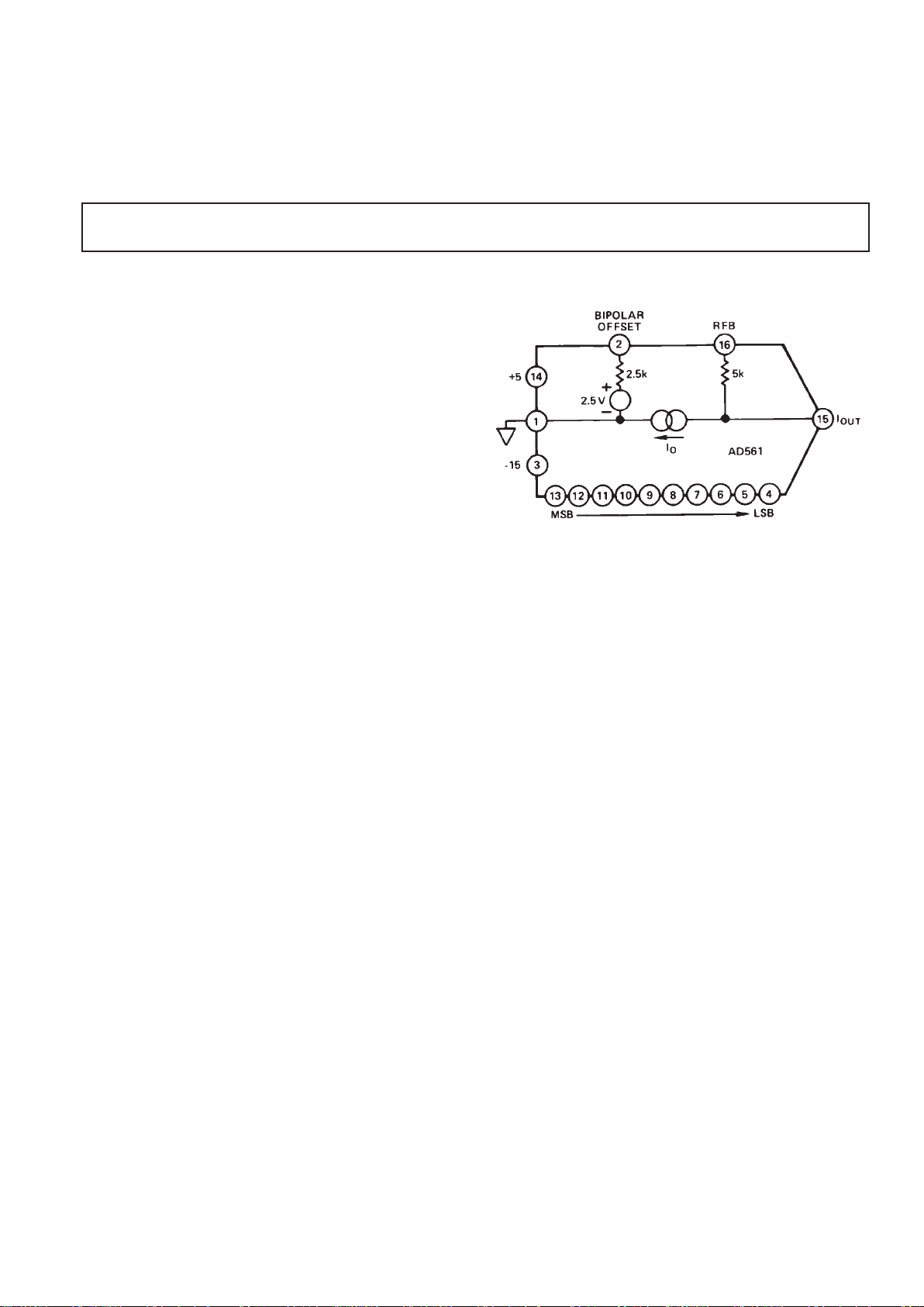
FUNCTIONAL BLOCK DIAGRAM
TO-116
PRODUCT DESCRIPTION
The AD561 is an integrated circuit 10-bit digital-to-analog
converter combined with a high stability voltage reference
fabricated on a single monolithic chip. Using ten precision highspeed current-steering switches, a control amplifier, voltage
reference, and laser-trimmed thin-film SiCr resistor network,
the device produces a fast, accurate analog output current.
Laser trimmed output application resistors are also included to
facilitate accurate, stable current-to-voltage conversion; they are
trimmed to 0.1% accuracy, thus eliminating external trimmers
in many situations.
Several important technologies combine to make the AD561 the
most accurate and most stable 10-bit DAC available. The low
temperature coefficient, high stability thin-film network is
trimmed at the wafer level by a fine resolution laser system to
0.01% typical linearity. This results in an accuracy specification
of ±1/4 LSB max for the K and T versions, and 1/2 LSB max
for the J and S versions.
The AD561 also incorporates a low noise, high stability
subsurface zener diode to produce a reference voltage with
excellent long term stability and temperature cycle characteristics, which challenge the best discrete Zener references. A
temperature compensation circuit is laser-trimmed to allow
custom correction of the temperature coefficient of each device.
This results in a typical full-scale temperature coefficient of
15 ppm/°C; the TC is tested and guaranteed to 30 ppm/°C max
for the K and T versions, 60 ppm/°C max for the S, and
80 ppm/°C for the J.
The AD561 is available in four performance grades. The
AD561J and K are specified for use over the 0°C to +70°C
temperature range and are available in either a 16-pin
FEATURES
Complete Current Output Converter
High Stability Buried Zener Reference
Laser Trimmed to High Accuracy (1/4 LSB Max Error,
AD561K, T)
Trimmed Output Application Resistors for 0 V to +10 V,
65 V Ranges
Fast Settling – 250 ns to 1/2 LSB
Guaranteed Monotonicity Over Full Operating
Temperature Range
TTL/DTL and CMOS Compatible (Positive True Logic)
Single Chip Monolithic Construction
Available in Chip Form
MlL-STD-883-Compliant Versions Available
hermetically-sealed ceramic DIP or a 16-pin molded plastic
DIP. The AD561S and T grades are specified for the –55°C to
+125°C range and are available in the ceramic package.
PRODUCT HIGHLIGHTS
1. Advanced monolithic processing and laser trimming at the
wafer level have made the AD561 the most accurate 10-bit
converter available, while keeping costs consistent with large
volume integrated circuit production. The AD561K and T
have 1/4 LSB max relative accuracy and 1/2 LSB max
differential nonlinearity. The low TC R-2R ladder guarantees that all AD561 units will be monotonic over the entire
operating temperature range.
2. Digital system interfacing is simplified by the use of a
positive true straight binary code. The digital input voltage
threshold is a function of the positive supply level; connecting V
CC
to the digital logic supply automatically sets the
threshold to the proper level for the logic family being used.
Logic sink current requirement is only 25 µA.
3. The high speed current steering switches are designed to settle
in less than 250 ns for the worst case digital code transition.
This allows construction of successive-approximation A/D
converters in the 3 µs to 5 µs range.
4. The AD561 has an output voltage compliance range from
–2 V to +10 V, allowing direct current-to-voltage conversion
with just an output resistor, omitting the op amp. The 40 MΩ
open collector output impedance results in negligible errors
due to output leakage currents.
5. The AD561 is available in versions compliant with MILSTD-883. Refer to the Analog Devices Military Products
Databook or current AD561/883B data sheet for detailed
specifications.

–2–
REV. A
AD561–SPECIFICATIONS
AD561J AD561K
Model Min Typ Max Min Typ Max Units
RESOLUTION 10 Bits 10 Bits
ACCURACY (Error Relative ±1/4 ±1/2 ±1/8 ±1/4 LSB
to Full Scale) (0.025) (0.05) (0.012) (0.025) % of FS
DIFFERENTIAL NONLINEARITY ±1/2 ±1/4 ±1/2 LSB
DATA INPUTS
TTL, V
CC
= +5 V
Bit ON Logic “1” +2.0 * V
Bit OFF Logic “0” +0.8 * V
CMOS, 10 V ≤ V
CC
≤ 16.5 V
Bit ON Logic “ 1 “ 70% V
CC
*V
Bit OFF Logic “0” 30% V
CC
*V
Logic Current (Each Bit) (T
MIN
to T
MAX
)
Bit ON Logic “1” +5 +100 * * nA
Bit OFF Logic “0” –5 –25 * * µA
OUTPUT
Current
Unipolar 1.5 2.0 2.4 * * * mA
Bipolar ±0.75 ±1.0 ±1.2 * * * mA
Resistance (Exclusive of
Application Resistors) 40 M * Ω
Unipolar Zero (All Bits OFF) 0.01 0.05 * * % of FS
Capacitance 25 * pF
Compliance Voltage –2 –3 +10 * * * V
SETTLING TIME TO 1/2 LSB
All Bits ON-to-OFF or OFF-to-ON 250 * ns
POWER REQUIREMENTS
V
CC
, +4.5 V dc to +16.5 V dc 8 10 * * mA
VEE, –10.8 V dc to –16.5 V dc 12 16 * * mA
POWER SUPPLY GAIN SENSITIVITY
V
CC
, +4.5 V dc to +16.5 V dc 2 10 * * ppm of FS/%
VEE, –10.8 V dc to –16.5 V dc 4 25 * * ppm of FS/%
TEMPERATURE RANGE
Operating 0 to +70 * * °C
Storage (“D” Package) –65 to +150 * * °C
(“N” Package) –25 to +85 * * °C
TEMPERATURE COEFFICIENTS
With Internal Reference
Unipolar Zero 1 10 1 5 ppm of FS/°C
Bipolar Zero 2 20 2 10 ppm of FS/°C
Full Scale 15 80 15 30 ppm of FS/°C
Differential Nonlinearity 2.5 2.5 ppm of FS/°C
MONOTONICITY Guaranteed Over Full Operating Guaranteed Over Full Operating
Temperature Range Temperature Range
PROGRAMMABLE OUTPUT 0 to +10 * V
RANGES –5 to +5 * V
CALIBRATION ACCURACY
Full-Scale Error with Fixed 25 Ω `
Resistor ±0.1 * % of FS
Bipolar Zero Error with Fixed 10 Ω
Resistor ±0.1 * % of FS
CALIBRATION ADJUSTMENT
RANGE
Full Scale (With 50 Ω Trimmer) ±0.5 * % of FS
Bipolar Zero (With 50 Ω Trimmer) ±0.5 * % of FS
NOTES
*Specifications same as AD561J specifications.
Specifications subject to change without notice.
(TA = +258C, VCC = –15 V, unless otherwise noted.)

–3–
REV. A
AD561
AD561S AD561T
Model Min Typ Max Min Typ Max Units
RESOLUTION 10 Bits 10 Bits
ACCURACY (Error Relative ±1/4 ±1/2 ±1/8 ±1/4 LSB
to Full Scale) (0.025) (0.05) (0.012) (0.025) % of FS
DIFFERENTIAL NONLINEARITY ±1/2 ±1/4 ±1/2 LSB
DATA INPUTS
TTL, V
CC
= +5 V
Bit ON Logic “1” +2.0 ** V
Bit OFF Logic “0” +0.8 ** V
CMOS, 10 V ≤ V
CC
≤ 16.5 V
Bit ON Logic “ 1 “ 70% V
CC
** V
Bit OFF Logic “0” 30% V
CC
** V
Logic Current (Each Bit) (T
MIN
to T
MAX
)
Bit ON Logic “1” +20 +100 ** ** nA
Bit OFF Logic “0” –25 –100 ** ** µA
OUTPUT
Current
Unipolar 1.5 2.0 2.4 ** ** ** mA
Bipolar ±0.75 ±1.0 ±1.2 ** ** ** mA
Resistance (Exclusive of
Application Resistors) 40 M ** Ω
Unipolar Zero (All Bits OFF) 0.01 0.05 ** ** % of FS
Capacitance 25 ** pF
Compliance Voltage –2 –3 +10 ** ** ** V
SETTLING TIME TO 1/2 LSB
All Bits ON-to-OFF or OFF-to-ON 250 ** ns
POWER REQUIREMENTS
V
CC
, +4.5 V dc to +16.5 V dc 6 10 ** ** mA
VEE, –10.8 V dc to –16.5 V dc 11 16 ** ** mA
POWER SUPPLY GAIN SENSITIVITY
V
CC
, +4.5 V dc to +16.5 V dc 2 10 ** ** ppm of FS/%
VEE, –10.8 V dc to –16.5 V dc 4 25 ** ** ppm of FS/%
TEMPERATURE RANGE
Operating –55 to +125 ** ** °C
Storage –65 to +150 ** ** °C
TEMPERATURE COEFFICIENTS
With Internal Reference
Unipolar Zero 1 10 1 5 ppm of FS/°C
Bipolar Zero 2 20 2 10 ppm of FS/°C
Full Scale 15 60 15 30 ppm of FS/°C
Differential Nonlinearity 2.5 2.5 ppm of FS/°C
MONOTONICITY Guaranteed Over Full Operating Guaranteed Over Full Operating
Temperature Range Temperature Range
PROGRAMMABLE OUTPUT 0 to +10 ** V
RANGES –5 to +5 ** V
CALIBRATION ACCURACY
Full-Scale Error with Fixed 25 Ω
Resistor ±0.1 ** % of FS
Bipolar Zero Error with Fixed 10 Ω
Resistor ±0.1 ** % of FS
CALIBRATION ADJUSTMENT
RANGE
Full Scale (With 50 Ω Trimmer) ±0.5 ** % of FS
Bipolar Zero (With 50 Ω Trimmer) ±0.5 ** % of FS
NOTES
**Specifications same as AD561S specifications.
Specifications subject to change without notice.
 Loading...