


 Loading...
a |
12-Bit Ultrahigh Speed |
|
Monolithic D/A Converter |
||
|
|
|
|
|
AD568 |
|
|
|
|
FEATURES |
FUNCTIONAL BLOCK DIAGRAM |
|
Ultrahigh Speed: Current Settling to 1 LSB in 35 ns |
|
|
High Stability Buried Zener Reference on Chip |
|
|
Monotonicity Guaranteed Over Temperature |
|
|
10.24 mA Full-Scale Output Suitable for Video |
|
|
Applications |
|
|
Integral and Differential Linearity Guaranteed Over |
|
|
Temperature |
|
|
0.3" “Skinny DIP” Packaging |
|
|
Variable Threshold Allows TTL and CMOS |
|
|
Interface |
|
|
MIL-STD-883 Compliant Versions Available |
|
PRODUCT DESCRIPTION
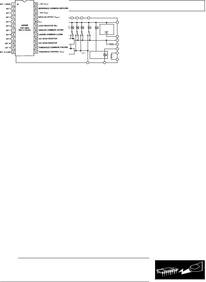
The AD568 is an ultrahigh-speed, 12-bit digital-to-analog converter (DAC) settling to 0.025% in 35 ns. The monolithic device is fabricated using Analog Devices’ Complementary Bipolar (CB) Process. This is a proprietary process featuring high-speed NPN and PNP devices on the same chip without the use of dielectric isolation or multichip hybrid techniques. The high speed of the AD568 is maintained by keeping impedance levels low enough to minimize the effects of parasitic circuit capacitances.
The DAC consists of 16 current sources configured to deliver a 10.24 mA full-scale current. Multiple matched current sources and thin-film ladder techniques are combined to produce bit weighting. The DAC’s output is a 10.24 mA full scale (FS) for current output applications or a 1.024 V FS unbuffered voltage output. Additionally, a 10.24 V FS buffered output may be generated using an onboard 1 kΩ span resistor with an external op amp. Bipolar ranges are accomplished by pin strapping.
Laser wafer trimming insures full 12-bit linearity. All grades of the AD568 are guaranteed monotonic over their full operating temperature range. Furthermore, the output resistance of the DAC is trimmed to 100 Ω ± 1.0%. The gain temperature coefficient of the voltage output is 30 ppm/°C max (K).
The AD568 is available in three performance grades. The AD568JQ and KQ are available in 24-pin cerdip (0.3") packages and are specified for operation from 0°C to +70°C. The AD568SQ features operation from –55°C to +125°C and is also packaged in the hermetic 0.3" cerdip.
PRODUCT HIGHLIGHTS
1.The ultrafast settling time of the AD568 allows leading edge performance in waveform generation, graphics display and high speed A/D conversion applications.
2.Pin strapping provides a variety of voltage and current output ranges for application versatility. Tight control of the absolute output current reduces trim requirements in externallyscaled applications.
3.Matched on-chip resistors can be used for precision scaling in high speed A/D conversion circuits.
4.The digital inputs are compatible with TTL and +5 V CMOS logic families.
5.Skinny DIP (0.3") packaging minimizes board space requirements and eases layout considerations.
6.The AD568 is available in versions compliant with MIL- STD-883. Refer to the Analog Devices Military Products Databook or current AD568/883B data sheet for detailed specifications.
REV. A
Information furnished by Analog Devices is believed to be accurate and reliable. However, no responsibility is assumed by Analog Devices for its use, nor for any infringements of patents or other rights of third parties which may result from its use. No license is granted by implication or otherwise under any patent or patent rights of Analog Devices.
One Technology Way, P.O. Box 9106, Norwood, MA 02062-9106, U.S.A. Tel: 617/329-4700 Fax: 617/326-8703

AD568–SPECIFICATIONS (@ = +258C, VCC, VEE = 615 V unless otherwise noted)
Model |
|
AD568J |
|
|
|
AD568K |
|
|
|
AD568S |
|
|
|
Min |
Typ |
Max |
|
Min |
Typ |
Max |
Min |
Typ |
Max |
Units |
|
|
|
|
|
|
|
|
|
|
|
|
|
|
RESOLUTION |
12 |
|
|
|
12 |
|
|
|
12 |
|
|
Bits |
|
|
|
|
|
|
|
|
|
|
|
|
|
ACCURACY1 |
–1/2 |
|
+1/2 |
|
–1/4 |
|
+1/4 |
|
–1/2 |
|
+1/2 |
|
Linearity |
|
|
|
|
|
LSB |
||||||
TMIN to TMAX |
–3/4 |
|
+3/4 |
|
–1/2 |
|
+1/2 |
|
–3/4 |
|
+3/4 |
LSB |
Differential Nonlinearity |
–1 |
|
+1 |
|
–1/2 |
|
+1/2 |
|
–1 |
|
+1 |
LSB |
TMIN to TMAX |
–1 |
|
+1 |
|
–1 |
|
+ 1 |
|
–1 |
|
–1 |
LSB |
|
|
|
|
|||||||||
Monotonicity |
GUARANTEED OVER RATED SPECIFICATION TEMPERATURE RANGE |
|
||||||||||
Unipolar Offset |
–0.2 |
|
+0.2 |
* |
|
* |
|
* |
|
* |
% of FSR |
|
|
|
|
|
|||||||||
Bipolar Offset |
–1.0 |
|
+1.0 |
* |
|
* |
|
* |
|
* |
% of FSR |
|
Bipolar Zero |
–0.2 |
|
+0.2 |
* |
|
* |
|
* |
|
* |
% of FSR |
|
Gain Error |
–1.0 |
|
+1.0 |
* |
|
* |
|
* |
|
* |
% of FSR |
|
|
|
|
|
|
|
|
|
|
|
|
|
|
TEMPERATURE COEFFICIENTS2 |
–5 |
|
+5 |
|
–3 |
|
+3 |
|
–5 |
|
+5 |
ppm of FSR/°C |
Unipolar Offset |
|
|
|
|
|
|||||||
Bipolar Offset |
–30 |
|
+30 |
|
–20 |
|
+20 |
|
–30 |
|
+30 |
ppm of FSR/°C |
Bipolar Zero |
–15 |
|
+15 |
|
• |
|
• |
|
• |
|
• |
ppm of FSR/°C |
Gain Drift |
–50 |
|
+50 |
|
–30 |
|
+30 |
|
–50 |
|
+50 |
ppm of FSR/°C |
Gain Drift (IOUT) |
–150 |
|
+150 |
* |
|
* |
|
* |
|
* |
ppm of FSR/°C |
|
|
|
|
|
|
|
|
|
|
|
|
|
|
DATA INPUTS |
|
|
|
|
|
|
|
|
|
|
|
|
Logic Levels (TMIN to TMAX) |
2.0 |
|
|
|
|
|
|
|
|
|
|
|
VIH |
|
7.0 |
* |
|
* |
|
* |
|
* |
V |
||
VIL |
0.0 |
|
0.8 |
* |
|
* |
|
* |
|
* |
V |
|
Logic Currents (TMIN to TMAX) |
–10 |
0 |
+10 |
|
|
|
|
|
|
|
|
μA |
IIH |
* |
* |
* |
|
* |
* |
* |
|||||
IIL |
–0.5 |
–60 |
–100 |
* |
* |
* |
|
* |
–100 |
–200 |
μA |
|
VTH Pin Voltage |
|
1.4 |
|
|
|
* |
|
|
|
* |
|
V |
CODING |
|
|
|
|
BINARY, OFFSET BINARY |
|
|
|
|
|||
|
|
|
|
|
|
|
|
|
|
|
|
|
CURRENT OUTPUT RANGES |
|
|
|
|
0 to 10.24, ±5.12 |
|
|
|
|
|
mA |
|
|
|
|
|
|
|
|
|
|
|
|
|
|
VOLTAGE OUTPUT RANGES |
|
|
|
|
0 to 1.024, ±0.512 |
|
|
|
|
|
V |
|
COMPLIANCE VOLTAGE |
–2 |
|
+1.2 |
|
* |
|
* |
|
* |
|
* |
V |
|
|
|
|
|
|
|
|
|
|
|
|
|
OUTPUT RESISTANCE |
|
|
|
|
|
|
|
|
|
|
|
Ω |
Exclusive of RL |
160 |
200 |
240 |
|
|
* |
|
|
|
* |
|
|
Inclusive of RL |
99 |
100 |
101 |
|
|
* |
|
|
|
* |
|
Ω |
|
|
|
|
|
|
|
|
|
|
|
|
|
SETTLING TIME |
|
|
|
|
|
|
|
|
|
|
|
|
Current to |
|
|
|
|
|
|
|
|
|
|
|
|
± 0.025% |
|
35 |
|
|
|
* |
|
|
|
* |
|
ns to 0.025% of FSR |
± 0.1% |
|
23 |
|
|
|
* |
|
|
|
* |
|
ns to 0.1% of FSR |
Voltage |
|
|
|
|
|
|
|
|
|
|
|
|
50 Ω Load3, 0.512 V p-p, |
|
|
|
|
|
|
|
|
|
|
|
|
to 0.025% |
|
37 |
|
|
|
* |
|
|
|
* |
|
ns to 0.025% of FSR |
to 0.1% |
|
25 |
|
|
|
* |
|
|
|
* |
|
ns to 0.1% of FSR |
to 1% |
|
18 |
|
|
|
* |
|
|
|
* |
|
ns to 1% of FSR |
75 Ω Load3, 0.768 V p-p, |
|
|
|
|
|
|
|
|
|
|
|
|
to 0.025% |
|
40 |
|
|
|
* |
|
|
|
* |
|
ns to 0.025% of FSR |
to 0.1% |
|
25 |
|
|
|
* |
|
|
|
* |
|
ns to 0.1% of FSR |
to 1% |
|
20 |
|
|
|
* |
|
|
|
* |
|
ns to 1% of FSR |
100 Ω (Internal RL)3, 1.024 V p-p, |
|
|
|
|
|
|
|
|
|
|
|
|
to 0.025% |
|
50 |
|
|
|
* |
|
|
|
* |
|
ns to 0.025% of FSR |
to 0.1% |
|
38 |
|
|
|
* |
|
|
|
* |
|
ns to 0.1% of FSR |
to 1% |
|
24 |
|
|
|
* |
|
|
|
* |
|
ns to 1% of FSR |
Glitch Impulse4 |
|
350 |
|
|
|
* |
|
|
|
* |
|
pV-sec |
Peak Amplitude |
|
15 |
|
|
|
* |
|
|
|
* |
|
% of FSR |
|
|
|
|
|
|
|
|
|
|
|
|
|
FULL-SCALE TRANSlTlON5 |
|
|
|
|
|
|
|
|
|
|
|
|
10% to 90% Rise Time |
|
11 |
|
|
|
* |
|
|
|
* |
|
ns |
90% to 10% Fall Time |
|
11 |
|
|
|
* |
|
|
|
* |
|
ns |
|
|
|
|
|
|
|
|
|
|
|
|
|
POWER REQUIREMENTS |
|
|
32 |
|
|
|
|
|
|
|
|
|
+13.5 V to +16.5 V |
|
27 |
|
|
* |
* |
|
|
* |
* |
mA |
|
–13.5 V to –16.5 V |
|
–7 |
–8 |
|
|
* |
* |
|
|
* |
* |
mA |
Power Dissipation |
|
525 |
625 |
|
|
* |
* |
|
|
* |
* |
mW |
PSRR |
|
|
0.05 |
|
|
|
* |
|
|
|
* |
% of FSR/V |
|
|
|
|
|
|
|
|
|
|
|
|
|
TEMPERATURE RANGE |
|
|
|
|
|
|
|
|
|
|
|
°C |
Rated Specification2 |
0 |
|
+70 |
|
0 |
|
+70 |
|
–55 |
|
+125 |
|
Storage |
–65 |
|
+150 |
|
* |
|
* |
|
* |
|
* |
°C |
NOTES
*Same as AD568J. 1Measured in IOUT mode.
2Measured in VOUT mode, unless otherwise specified. See text for further information. 3Total Resistance. Refer to Figure 3,
4At the major carry, driven by HCMOS logic. See text for further explanation. 5Measured in VOUT mode.
Specifications shown in boldface are tested on all production units at final electrical test. Specifications subject to change without notice.
–2– |
REV. A |
AD568
|
LSB |
|
|
|
|
|
|
|
|
|
|
MSB |
|
|
PIN CONFIGURATION |
|
12 |
11 |
10 |
9 |
8 |
7 |
6 |
5 |
4 |
3 |
2 |
1 |
|
|
|
|
PNP |
|
|
|
|
|
|
|
|
|
|
|
|
24 |
VCC |
|
CURRENT |
|
|
|
|
|
|
|
|
|
2X |
4X |
|
||
|
SOURCES |
|
|
|
|
|
|
|
|
|
BURIED |
|
|
||
|
|
|
|
|
|
|
|
|
|
|
|
|
|
||
|
PNP |
|
|
|
|
|
|
|
|
|
|
|
ZENER |
|
|
|
|
|
|
|
|
|
|
|
|
|
REFERENCE |
|
|
||
|
SWITCHES |
|
|
|
|
|
|
|
|
|
|
|
|
||
THRESHOLD |
|
|
|
|
|
|
|
|
|
|
|
|
|
|
|
13 |
|
|
|
|
|
|
|
|
|
|
|
|
|
REFERENCE |
|
CONTROL |
1.4V |
|
|
|
|
|
|
|
|
|
|
|
|
23 |
|
|
|
|
|
|
|
|
|
|
|
|
IOUT |
|
COMMON |
||
|
BAND- |
|
THIN-FILM R-2R LADDER |
|
|
|
|
|
20 |
IOUT |
|||||
|
GAP |
|
|
|
|
|
|
|
|||||||
|
REF |
|
|
(100 - 200Ω) |
|
|
|
|
|
|
200Ω |
LOAD RESISTOR |
|||
THRESHOLD |
|
|
|
|
|
|
|
|
|
|
|
|
|
19 |
(RL) |
|
|
|
|
|
|
|
|
|
|
|
|
|
|
||
COMMON 14 |
|
|
|
|
|
|
|
|
|
|
|
|
21 |
BIPOLAR |
|
LADDER |
17 |
|
DIFFUSED R-2R LADDER |
|
|
|
|
BIPOLAR |
|
|
OFFSET (IBPO) |
||||
COMMON |
|
|
|
(10 - 20Ω) |
|
|
|
|
IOUT |
|
15 |
10V SPAN |
|||
|
|
|
|
|
|
|
|
|
|
CURRENT |
|
1kΩ |
RESISTOR |
||
|
|
|
|
|
|
|
|
|
|
|
|
||||
|
|
|
|
|
|
|
|
|
|
|
|
GENERATOR |
10V SPAN |
||
|
AD568 |
|
|
|
|
|
|
|
|
|
|
|
|
16 |
|
|
|
|
|
|
|
|
|
|
|
|
|
18 |
22 |
|
RESISTOR |
|
|
|
|
|
|
|
|
|
|
|
|
|
|
||
|
|
|
|
|
|
|
|
|
|
|
ANALOG |
VEE |
|
|
|
|
|
|
|
|
|
|
|
|
|
|
COMMON |
|
|
|
|
Figure 1. Functional Block Diagram
ABSOLUTE MAXIMUM RATINGS1 |
|
VCC to REFCOM . . . . . . . . . . . . . . . . . . . |
. . . . . 0 V to +18 V |
VEE to REFCOM . . . . . . . . . . . . . . . . . . . . . |
. . . . 0 V to –18 V |
REFCOM to LCOM . . . . . . . . . . . . . . . . . |
+100 mV to –10 V |
ACOM to LCOM . . . . . . . . . . . . . . . . . . . . |
. . . . . . . ±100 mV |
THCOM to LCOM . . . . . . . . . . . . . . . . . . . |
. . . . . . . ±500 mV |
SPANs to LCOM . . . . . . . . . . . . . . . . . . . . |
. . . . . . . . . ±12 V |
IBPO to LCOM . . . . . . . . . . . . . . . . . . . . . . . |
. . . . . . . . . . ±5 V |
IOUT to LCOM . . . . . . . . . . . . . . . . . . . . . . |
. . . . . –5 V to VTH |
Digital Inputs to THCOM . . . . . . . . . . . . . |
–500 mV to +7.0 V |
Voltage Across Span Resistor . . . . . . . . . . . . |
. . . . . . . . . . 12 V |
VTH to THCOM . . . . . . . . . . . . . . . . . . . . . |
. –0.7 V to +1.4 V |
Logic Threshold Control Input Current . . . |
. . . . . . . . . . 5 mA |
Power Dissipation . . . . . . . . . . . . . . . . . . . . . . . . . . . 100 mW
Storage Temperature Range
Q (Cerdip) Package . . . . . . . . . . . . . . . . . –65°C to +150°C
Junction Temperature . . . . . . . . . . . . . . . . . . . . . . . . . . 175°C
Thermal Resistance
θJA . . . . . . . . . . . . . . . . . . . . . . . . . . . . . . . . . . . . . . 75°C/W
θJC . . . . . . . . . . . . . . . . . . . . . . . . . . . . . . . . . . . . . . 25°C/W
1Stresses above those listed under “Absolute Maximum Ratings” may cause permanent damage to the device. This is a stress rating only and functional operation of the device at these or any other conditions above those indicated in the operational section of this specification is not implied. Exposure to absolute maximum rating conditions for extended periods may affect device reliability.
ORDERING GUIDE
|
|
|
Linearity |
Voltage |
Modell |
Package Option2 |
Temperature |
Error Max |
Gain T.C. |
Range 8C |
@ 258C |
Max ppm/8C |
||
|
|
|
|
|
AD568JQ |
24-Lead Cerdip (Q-24) |
0 to +70 |
±1/2 |
±50 |
AD568KQ |
24-Lead Cerdip (Q-24) |
0 to +70 |
±1/4 |
±30 |
AD568SQ |
24-Lead Cerdip (Q-24) |
–55 to +125 |
±1/2 |
±50 |
NOTES
1For details on grade and package offerings screened in accordance with MIL-STD-883, refer to the Analog Devices Military Products Databook or current AD568/883B data sheet.
2Q = Cerdip.
Definitions
LINEARITY ERROR (also called INTEGRAL NONLINEARITY OR INL): Analog Devices defines linearity error as the maximum deviation of the actual analog output from the ideal output (a straight line drawn from 0 to FS) for any bit combination expressed in multiples of 1 LSB. The AD568 is laser trimmed to 1/4 LSB (0.006% of FS) maximum linearity error at +25°C for the K version and 1/2 LSB for the J and S versions.
DIFFERENTIAL LINEARITY ERROR (also called DIFFERENTIAL NONLINEARITY or DNL): DNL is the measure of the variation in analog value, normalized to full scale, associated with a 1 LSB change in digital input code. Monotonic behavior
requires that the differential linearity error not exceed 1 LSB in the negative direction.
MONOTONICITY: A DAC is said to be monotonic if the output either increases or remains constant as the digital input increases.
UNIPOLAR OFFSET ERROR: The deviation of the analog output from the ideal (0 V or 0 mA) when the inputs are set to all 0s is called unipolar offset error.
BIPOLAR OFFSET ERROR: The deviation of the analog output from the ideal (negative half-scale) when the inputs are set to all 0s is called bipolar offset error.
CAUTION
ESD (electrostatic discharge) sensitive device. Electrostatic charges as high as 4000 V readily accumulate on the human body and test equipment and can discharge without detection. Although the AD568 features proprietary ESD protection circuitry, permanent damage may occur on devices subjected to high energy electrostatic discharges. Therefore, proper ESD precautions are recommended to avoid performance degradation or loss of functionality.
WARNING!
ESD SENSITIVE DEVICE
REV. A |
–3– |
AD568
BIPOLAR ZERO ERROR: The deviation of the analog output from the ideal half-scale output of 0 V (or 0 mA) for bipolar mode when only the MSB is on (100 . . .00) is called bipolar zero error.
GAIN ERROR: The difference between the ideal and actual output span of FS –1 LSB, expressed in % of FS, or LSB, when all bits are on.
GLITCH IMPULSE: Asymmetrical switching times in a DAC give rise to undesired output transients which are quantified by
their glitch impulse. It is specified as the net area of the glitch in nV-sec or pA-sec.
COMPLIANCE VOLTAGE: The range of allowable voltage at the output of a current-output DAC which will not degrade the accuracy of the output current.
SETTLING TIME: The time required for the output to reach and remain within a specified error band about its final value, measured from the digital input transition.
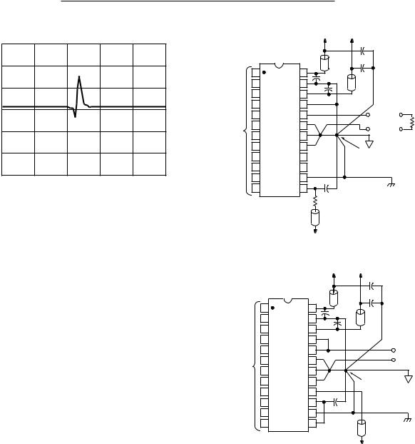
|
0.8 |
|
|
|
|
|
OUTPUT – VOLTS |
0.6 |
|
|
|
|
|
0.4 |
|
|
|
|
|
|
|
0 |
50 |
100 |
150 |
200 |
250 |
TIME – ns
Figure 2. Glitch Impulse
Connecting the AD568
|
|
|
+15V |
–15V |
|
|
|
|
|
0.2µF |
|
|
|
|
|
0.1µF |
|
|
1 |
+15V 24 |
FERRITE BEADS |
||
|
|
|
0.1µF |
STACKPOLE 57-1392 |
|
|
2 |
REFCOM 23 |
OR |
|
|
|
3 |
–15V |
0.1µF |
AMIDON FB-43B-101 |
|
|
22 |
OR EQUIVALENT |
|||
|
|
|
|
||
|
4 |
IBPO 21 |
|
|
|
|
5 |
IOUT 20 |
ANALOG |
REXT |
|
|
6 |
AD568 RL |
|
||
DIGITAL |
19 |
OUTPUT |
(OPTIONAL) |
||
INPUTS |
7 |
ACOM 18 |
ANALOG |
||
|
|||||
|
|
|
|
||
|
8 |
LCOM 17 |
SUPPLY GROUND |
||
|
9 |
SPAN 16 NC |
ANALOG |
|
|
|
GND PLANE |
|
|||
|
10 |
SPAN 15 NC |
DIGITAL |
DIGITAL |
|
|
11 |
THCOM 14 |
GND PLANE |
||
|
|
SUPPLY |
|||
|
|
|
100pF |
|
GROUND |
|
12 |
VTH 13 |
|
||
|
|
|
|||
|
|
|
RTH |
|
|
|
|
|
1kΩ |
|
|
|
|
|
+5V |
|
|
Figure 3. Unipolar Output Unbuffered 0 V to +1.024 V
UNBUFFERED VOLTAGE OUTPUT
Unipolar Configuration
Figure 3 shows the AD568 configured to provide a unipolar 0 to +1.024 V output range. In this mode, the bipolar offset terminal, Pin 21, should be grounded if not used for offset trimming.
The nominal output impedance of the AD568 with Pin 19 grounded has been trimmed to 100 Ω, ±1%. Other output impedances can be generated with an external resistor, REXT, between Pins 19 and 20. An REXT equalling 300 Ω will yield a total output resistance of 75 Ω, while an REXT of 100 Ω will provide 50 Ω of output resistance. Note that since the full-scale output current of the DAC remains 10.24 mA, changing the load impedance changes the unbuffered output voltage accordingly. Settling time and full-scale range characteristics for these load impedances are provided in the specifications table.
Bipolar Configuration
Figure 4 shows the connection scheme used to provide a bipolar output voltage range of 1.024 V. The bipolar offset (–0.512 V) occurs when all bits are OFF (00 . . . 00), bipolar zero (0 V) occurs when the MSB is ON with all other bits OFF (10 . . . 00), and full-scale minus 1 LSB (0.51175 V) is generated when all bits are ON (11 . . . 11). Figure 5 shows an optional bipolar mode with a 2.048 V range. The scale factor in this mode will not be as accurate as the configuration shown in Figure 4, because the laser-trimmed resistor RL is not used.
|
|
|
|
+15V |
–15V |
|
|
|
|
|
|
0.2µF |
|
|
|
|
|
|
0.1µF |
|
|
1 |
+15V |
24 |
0.1µF |
|
|
|
2 |
REFCOM 23 |
|
|
||
|
0.1µF |
|
|
|||
|
3 |
–15V |
22 |
|
|
|
|
|
|
|
|||
|
4 |
IBPO 21 |
|
|
|
|
|
5 |
IOUT 20 |
|
ANALOG |
||
DIGITAL |
6 |
AD568 RL |
19 |
|
OUTPUT |
|
INPUTS |
7 |
ACOM 18 |
|
|
ANALOG |
|
|
8 |
LCOM 17 |
|
ANALOG |
SUPPLY |
|
|
|
GROUND |
||||
|
9 |
SPAN 16 |
|
GND PLANE |
|
|
|
100pF |
|
|
|||
|
|
|
|
|
|
|
|
10 |
SPAN 15 |
|
DIGITAL |
|
|
|
11 |
THCOM 14 |
|
GND PLANE |
DIGITAL |
|
|
|
|
SUPPLY |
|||
|
|
|
|
|
|
|
|
12 |
VTH 13 |
|
|
GROUND |
|
|
|
|
|
|
+5V |
|
Figure 4. Bipolar Output Unbuffered ±0.512 V
Figure 4 also demonstrates how the internal span resistor may be used to bias the VTH pin (Pin 13) from a 5 V supply. This eliminates the requirement for an external RTH in applications that do not require the precision span resistor.
–4– |
REV. A |

AD568
|
|
|
+15V |
–15V |
|
|
|
|
|
0.2µF |
|
|
|
|
|
0.1µF |
|
|
1 |
+15V |
24 |
|
|
|
|
|
0.1µF |
|
|
|
2 |
REFCOM 23 |
|
|
|
|
3 |
–15V |
0.1µF |
|
|
|
22 |
|
|
||
|
4 |
IBPO 21 |
|
|
|
|
5 |
IOUT 20 |
ANALOG |
||
|
|
AD568 RL |
|
||
DIGITAL |
6 |
19 |
OUTPUT |
||
INPUTS |
7 |
ACOM 18 |
|
ANALOG |
|
|
|
||||
|
8 |
LCOM 17 |
|
SUPPLY |
|
|
ANALOG |
GROUND |
|||
|
|
|
|
||
|
9 |
SPAN 16 NC |
|
||
|
GND PLANE |
|
|||
|
10 |
SPAN 15 NC |
DIGITAL |
DIGITAL |
|
|
11 |
THCOM 14 |
GND PLANE |
||
|
|
SUPPLY |
|||
|
|
|
100pF |
|
GROUND |
|
12 |
VTH 13 |
|
||
|
|
|
|||
|
|
|
RTH |
|
|
|
|
|
1kΩ |
|
|
|
|
|
+5V |
|
|
Figure 5. Bipolar Output Unbuffered ±1.024 V
Optional Gan and Zero Adjustment
The gain and offset are laser trimmed to minimize their effects on circuit performance. However, in some applications, it may be desirable to externally reduce these errors further. In those cases, the following procedures are suggested.
UNIPOLAR MODE: (Refer to Figure 6)
Step 1 – Set all bits (BIT 1–BIT 12) to Logic “0” (OFF)—note the output voltage. This is the offset error.
Step 2 – Set all bits to Logic “1” (ON). Adjust the gain trim resistor so that the output voltage is equal to the desired full scale minus 1 LSB plus the offset error measured in step 1.
Step 3 – Reset all bits to Logic “0” (OFF). Adjust the offset trim resistor for 0 V output.
|
1 |
BIT 1 |
24 |
|
|
|
2 |
MSB |
23 |
|
|
|
|
|
|
||
|
3 |
AD568 |
22 |
|
|
|
4 |
IBPO 21 |
|
|
|
|
5 |
IOUT 20 |
|
|
|
|
6 |
RL |
GAIN |
5.11kΩ |
ANALOG |
DIGITAL |
19 |
||||
|
|
20Ω |
100Ω |
OUTPUT |
|
INPUTS |
|
|
|||
7 |
ACOM 18 |
(0 TO 1.024V) |
|||
|
8 |
LCOM 17 |
OFFSET |
|
|
|
|
|
|||
|
9 |
|
16 |
|
|
|
10 |
|
15 |
|
|
|
11 |
|
14 |
|
|
|
12 |
BIT 12 |
13 |
|
|
|
|
LSB |
|
|
|
Figure 6. Unbuffered Unipolar Gain and Zero Adjust
full scale at the DAC output. Note: this may slightly compromise the bipolar zero trim.
1 |
BIT 1 |
24 |
2 |
MSB |
23 |
|
|
3 |
AD568 |
22 |
|
VCC |
|
|
|
4 |
IBPO 21 |
|
|
|||
|
|
|
|
||||
|
5 |
IOUT 20 |
GAIN |
|
|
||
|
|
|
|
|
ANALOG |
||
DIGITAL |
6 |
RL |
19 |
5.11kΩ |
ZERO |
||
|
|||||||
|
|
|
20Ω |
20kΩ OUTPUT |
|||
INPUTS |
7 |
ACOM |
18 |
75Ω |
|
(–0.512 TO |
|
|
|
0.512V) |
|||||
|
8 |
LCOM 17 |
|
||||
|
|
|
|
||||
|
9 |
|
16 |
|
VEE |
|
|
|
10 |
|
15 |
|
|
||
|
|
|
|
|
|||
|
11 |
|
14 |
|
|
|
|
|
12 |
BIT 12 |
13 |
|
|
|
|
|
|
LSB |
|
|
|
|
|
Figure 7. Bipolar Unbuffered Gain and Zero Adjust
BUFFERED VOLTAGE OUTPUT
For full-scale outputs of greater than 1 V, some type of external buffer amplifier is required. The AD840 fills this requirement perfectly, settling to 0.025% from a 10 V full-scale step in less than 100 ns.
A 1 kΩ span resistor has been provided on chip for use as a feedback resistor in buffered applications. Using RSPAN (Pins 15, 16) introduces a 100 mW code-dependent power source onto the chip which may generate a slight degradation in linearity. Maximum linearity performance can be realized by using an external span resistor.
|
|
|
+15V |
–15V |
|
|
|
|
|
0.2µF |
|
|
|
|
|
0.1µF |
|
|
1 |
+15V |
24 |
|
|
|
|
|
0.1µF |
|
|
|
2 |
REFCOM 23 |
–VS |
+VS |
|
|
3 |
–15V |
0.1µF |
||
|
22 |
|
|
||
|
4 |
IBPO 21 |
|
AD840 |
|
|
5 |
IOUT 20 |
100Ω |
ANALOG |
|
|
|
AD568 RL |
|
|
|
DIGITAL |
6 |
19 |
|
OUTPUT |
|
INPUTS |
7 |
ACOM 18 |
|
|
|
|
|
|
|||
|
8 |
LCOM 17 |
ANALOG |
|
|
|
9 |
SPAN 16 |
GND PLANE |
ANALOG |
|
|
|
SUPPLY |
|||
|
|
|
5pF |
|
GROUND |
|
10 |
SPAN 15 |
|
||
|
|
|
|||
|
11 |
THCOM 14 |
DIGITAL |
|
|
|
|
|
100pF |
|
|
|
12 |
VTH 13 |
GND PLANE |
DIGITAL |
|
|
|
|
|
|
|
|
|
|
RTH |
|
SUPPLY |
|
|
|
1kΩ |
|
GROUND |
AMPLIFIER NOISE GAIN: 11
+5V
BIPOLAR MODE (Refer to Figure 7)
Step 1 – Set bits to offset binary “zero” (10 . . . 00). Adjust the zero resistor to produce 0 V at the DAC output. This removes the bipolar zero error.
Step 2 – Set all bits to Logic “1” (ON). Adjust gain trim resistor so the output voltage is equal to the desired full-scale minus
l LSB .
Step 3 – (Optional) If precise trimming of the bipolar offset is preferred to trimming of bipolar zero: set all bits to Logic “0” (OFF). Trim the zero resistor to produce the desired negative
REV. A
Figure 8. Unipolar Output Buffered 0 to –10.24V
Unipolar Inverting Configuration
Figure 8 shows the connections for producing a – 10.24 V fullscale swing. This configuration uses the AD568 in the current output mode into a summing junction at the inverting input terminal of the external op amp. With the load resistor RL grounded, the DAC has an output impedance of 100 Ω. This produces a noise gain of 11 from the noninverting terminal of the op amp, and hence, satisfies the stability criterion of the AD840 (stable at a gain of 10). The addition of a 5 pF compen-
–5–
Loading...