


AD544SH
Analog Devices AD544SH, AD544LH, AD544KH, AD544JH, AD542SH-883B Datasheet
...
REV. B
Information furnished by Analog Devices is believed to be accurate and
reliable. However, no responsibility is assumed by Analog Devices for its
use, nor for any infringements of patents or other rights of third parties
which may result from its use. No license is granted by implication or
otherwise under any patent or patent rights of Analog Devices.
a
High Performance,
BiFET Operational Amplifiers
AD542/AD544/AD547
One Technology Way, P.O. Box 9106, Norwood, MA 02062-9106, U.S.A.
Tel: 617/329-4700 Fax: 617/326-8703
CONNECTION DIAGRAM
+V
NULL
3
4
5
6
7
8
1
2
NULL
OUTPUTINVERTING
INPUT
NONINVERTING
INPUT
–V
TAB
NOTE: PIN 4 CONNECTED TO CASE
FEATURES
Ultralow Drift: 1 mV/8C (AD547L)
Low Offset Voltage: 0.25 mV (AD547L)
Low Input Bias Currents: 25 pA max
Low Quiescent Current: 1.5 mA
Low Noise: 2 mV p-p
High Open Loop Gain: 110 dB
High Slew Rate: 13 V/ms
Fast Settling to 60.01%: 3 ms
Low Total Harmonic Distortion: 0.0025%
Available in Hermetic Metal Can and Die Form
MIL-STD-883B Versions Available
Dual Versions Available: AD642, AD644, AD647
PRODUCT DESCRIPTION
The BiFET series of precision, monolithic FET-input op amps
are fabricated with the most advanced BiFET and laser trimming technologies. The AD542, AD544, AD547 series offers
bias currents significantly lower than currently available BiFET
devices, 25 pA max, warmed up.
In addition, the offset voltage is laser trimmed to less than
0.25 mV on the AD547L, which is achieved by utilizing Analog
Devices’ exclusive laser wafer trimming (LWT) process. When
combined with the AD547’s low offset drift (1 µV/°C), these
features offer the user performance superior to existing BiFET
op amps at low BiFET pricing.
The AD542 or AD547 is recommended for any operational amplifier application requiring excellent dc performance at low to
moderate cost. Precision instrument front ends requiring accurate amplification of millivolt level signals from megohm source
impedances will benefit from the device’s excellent combination
of low offset voltage and drift, low bias current and low 1/f
noise. High common-mode rejection (80 dB, min on the “K”
and “L” grades) and high open-loop gain, even under heavy
loading, ensures better than “12-bit” linearity in high impedance buffer applications.
The AD544 is recommended for any op amp applications requiring excellent ac and dc performance at low cost. The
2 MHz bandwidth and low offset of the AD544 make it the first
choice as an output amplifier for current output D/A converters,
such as the AD7541, 12-bit CMOS DAC.
Devices in this series are available in four grades: the “J,” “K,”
and “L” grades are specified over the 0°C to +70°C temperature
range and the “S” grade over the –55°C to +125°C operating
temperature range. All devices are offered in the hermetically
sealed, TO-99 metal can package.
PRODUCT HIGHLIGHTS
1. Improved bipolar and JFET processing results in the lowest
bias current available in a monolithic FET op amp.
2. Analog Devices, unlike some manufacturers, specifies each
device for the maximum bias current at either input in the
warmed-up condition, thus assuring the user that the device
will meet its published specifications in actual use.
3. Advanced laser wafer trimming techniques reduce offset voltage drift to 1 µV/°C max and offset voltage to only 0.25 mV
max on the AD547L.
4. Low voltage noise (2 µV p-p) and low offset voltage drift en-
hance performance as a precision op amp.
5. High slew rate (13 V/µs) and fast settling time to 0.01% (3 µs)
make the AD544 ideal for D/A, A/D, sample-hold circuits
and high speed integrators.
6. Low harmonic distortion (0.0025%) make the AD544 an
ideal choice in audio applications.
7. Bare die are available for use in hybrid circuit applications.

AD542 AD544 AD547
Parameter Min Typ Max Min Typ Max Min Typ Max Units
OPEN-LOOP GAIN
1
V
OUT
= ±10 V, RL = 2 kΩ
J Grade 100 30 100 V/mV
K, L, S Grades 250 50 250 V/mV
T
A
= T
MIN
to T
MAX
J Grade 100 20 100 V/mV
S Grade 100 20 100 V/mV
K, L Grades 250 40 250 V/mV
OUTPUT CHARACTERISTICS
R
L
= 2 kΩ
T
A
= T
MIN
to T
MAX
±
10 ±12
±
10 ±12
±
10 ±12 V
R
L
= 10 kΩ
T
A
= T
MIN
to T
MAX
±
12 ±13
±
12 ±13
±
12 ±13 V
Short Circuit Current 25 25 25 mA
FREQUENCY RESPONSE
Unity Gain, Small Signal 1.0 2.0 1.0 MHz
Full Power Response 50 200 50 kHz
Slew Rate, Unity Gain 2.0 3.0 8.0 13.0 2.0 3.0 V/µs
Total Harmonic Distortion 0.0025 %
INPUT OFFSET VOLTAGE
2
J Grade 2.0 2.0 1.0 mV
K Grade 1.0 1.0 0.5 mV
L Grade 0.5 0.5 0.25 mV
S Grade 1.0 1.0 0.5 mV
vs. Temperature
3
J Grade 20 20 5 µV/°C
K Grade 10 10 2 µV/°C
L Grade 551µV/°C
S Grade 15 15 5 µV/°C
vs. Supply, T
A
= T
MIN
to T
MAX
J Grade 200 200 200 µV/V
K, L, S Grades 100 100 100 µV/V
INPUT BIAS CURRENT
4
Either Input
J Grade 50 50 50 pA
K, L, S Grades 10 25 10 25 10 25 pA
Input Offset Current
J Grade 5 15 5 15 5 15 pA
K, L, S Grades 2 15 2 15 2 15 pA
INPUT IMPEDANCE
Differential 10
12
i610
12
i610
12
i6 ΩipF
Common Mode 1012i310
12
i310
12
i3 ΩipF
INPUT VOLTAGE
5
Differential ±20 ±20 ±20 V
Common Mode
±
10 ±12
±
10 ±12
±
10 ±12 V
Common-Mode Rejection
V
IN
= ±10 V
J Grade 76 76 76 dB
K, L, S Grades 80 80 80 dB
AD542/AD544/AD547–SPECIFICATIONS
REV. B
–2–
( VS = 615 V @ TA = +258C unless otherwise noted)

AD542/AD544/AD547
REV. B
–3–
AD542 AD544 AD547
Parameter Min Typ Max Min Typ Max Min Typ Max Units
POWER SUPPLY
Rated Performance ± 15 ±15 ± 15 V
Operating ± 5
±
18 ±5
±
18 ±5
±
18 V
Quiescent Current 1.1 1.5 1.8 2.5 1.1 1.5 mA
VOLTAGE NOISE
0.1 Hz to 10 Hz
J Grade 2.0 2.0 2.0 µV p-p
K, L, S Grades 2.0 2.0 4.0 µV p-p
10 Hz 70 35 70 nV/√
Hz
100 Hz 45 22 45 nV/√
Hz
1 kHz 30 18 30 nV/√
Hz
10 kHz 25 16 25 nV/√Hz
TEMPERATURE RANGE
Operating, Rated Performance
J, K, L Grades 0 to +70 0 to +70 0 to +70 °C
S Grade –55 to +125 –55 to +125 –55 to +125 °C
Storage –65 to +150 –65 to +150 –65 to +150 °C
TRANSISTOR COUNT 29 29 29
NOTES
1
Open-Loop Gain is specified with VOS both nulled and unnulled.
2
Input Offset Voltage specifications are guaranteed after 5 minutes of operation at TA = +25°C.
3
Input Offset Voltage Drift is specified with the offset voltage unnulled. Nulling will induce an additional 3 µV/°C/mV of nulled offset.
4
Bias Current specifications are guaranteed at either input after 5 minutes of operation at TA = +25°C. For higher temperatures, the current doubles every 10°C.
5
Defined as the maximum safe voltage between inputs, such that neither exceeds ± 10 V from ground.
Specifications subject to change without notice.
Specifications shown in boldface are tested on all production units at final electrical test. Results from those tests are used to calculate outgoing quality levels.
All min and max specifications are guaranteed, although only those shown in boldface are tested on all production units.
ORDERING GUIDE
Initial Offset Settling Time
Offset Voltage to 60.012% for Package Package
Model Voltage Drift a 10 V Step Description Option
AD542JCHIPS 2.0 mV 20 µV/°C5 µs Bare Die
AD542JH 2.0 mV 20 µV/°C5 µs 8-Pin Hermetic Metal Can H-08A
AD542KH 1.0 mV 10 µV/°C5 µs 8-Pin Hermetic Metal Can H-08A
AD542LH 0.5 mV 5 µV/°C5 µs 8-Pin Hermetic Metal Can H-08A
AD542SH 1.0 mV 15 µV/°C5 µs 8-Pin Hermetic Metal Can H-08A
AD542SH/883B 1.0 mV 15 µV/°C5 µs 8-Pin Hermetic Metal Can H-08A
AD544JH 2.0 mV 20 µV/°C3 µs 8-Pin Hermetic Metal Can H-08A
AD544KH 1.0 mV 10 µV/°C3 µs 8-Pin Hermetic Metal Can H-08A
AD544LH 0.5 mV 5 µV/°C3 µs 8-Pin Hermetic Metal Can H-08A
AD544SH 1.0 mV 15 µV/°C3 µs 8-Pin Hermetic Metal Can H-08A
AD544SH/883B 1.0 mV 15 µV/°C3 µs 8-Pin Hermetic Metal Can H-08A
AD547JH 1.0 mV 5 µV/°C5 µs 8-Pin Hermetic Metal Can H-08A
AD547KH 0.5 mV 2 µV/°C5 µs 8-Pin Hermetic Metal Can H-08A
AD547LH 0.25 mV 1 µV/°C5 µs 8-Pin Hermetic Metal Can H-08A
AD547SCHIPS 0.5 mV 5 µV/°C5 µs Bare Die
AD547SH/883B 0.5 mV 5 µV/°C5 µs 8-Pin Hermetic Metal Can H-08A
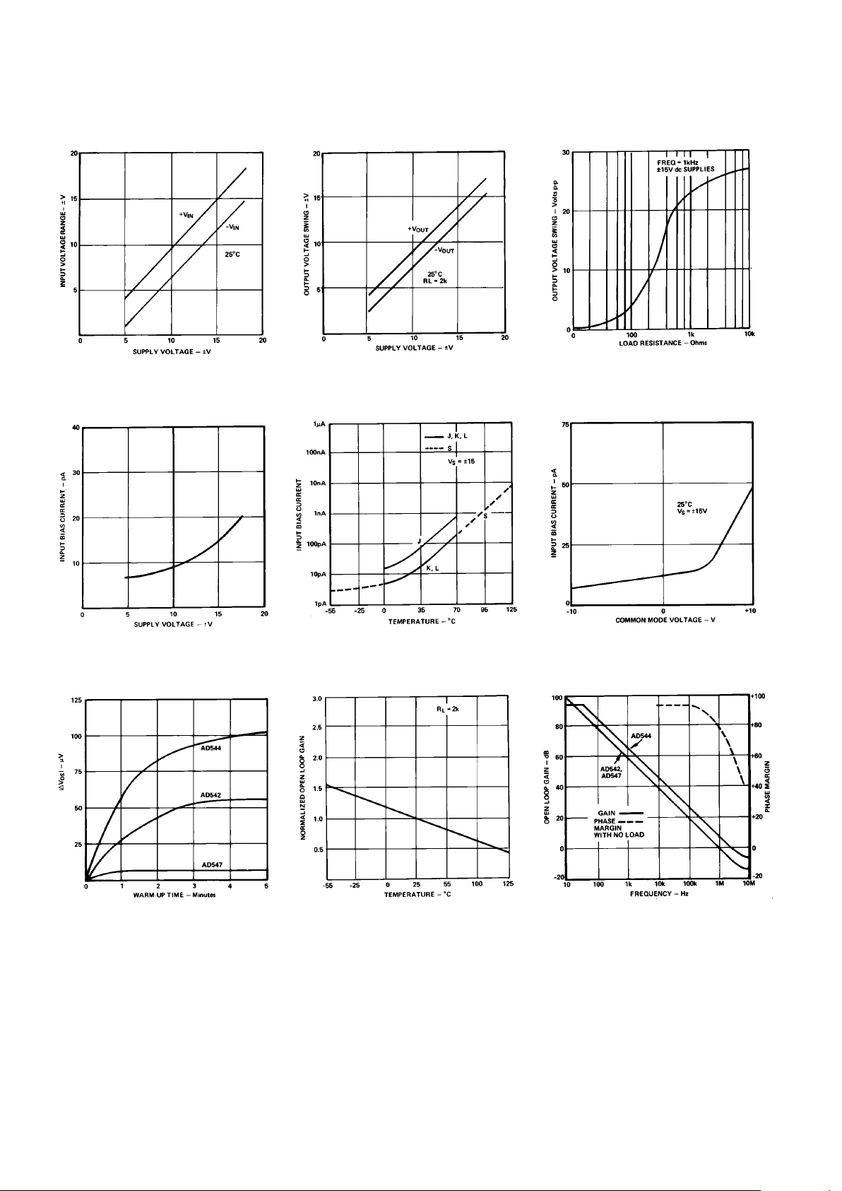
AD542/AD544/AD547–Typical Characteristics
Figure 1. Input Voltage Range vs.
Supply Voltage
Figure 4. Input Bias Current vs.
Supply Voltage
Figure 7. Change in Offset Voltage
vs. Warm-Up Time
Figure 2. Output Voltage Swing vs.
Supply Voltage
Figure 5. Input Bias Current vs.
Temperature
Figure 8. Open Loop Gain vs.
Temperature
Figure 3. Output Voltage Swing vs.
Load Resistance
Figure 6. Input Bias Current vs.
CMV
Figure 9. Open Loop Frequency
Response
REV. B
–4–
 Loading...