


 Loading...
|
2.7 V to 5.5 V, <100 µA, 8-/10-/12-Bit nanoDACs® with |
|
I2C®-Compatible Interface in LFCSP and SC70 |
Data Sheet |
AD5602/AD5612/AD5622 |
|
|
FEATURES
Single 8-, 10-, 12-bit DACs, 2 LSB INL 6-lead LFCSP and SC70 packages Micropower operation: 100 µA max @ 5 V Power-down to <150 nA @ 3 V
2.7 V to 5.5 V power supply Guaranteed monotonic by design
Power-on reset to 0 V with brownout detection 3 power-down functions
I2C-compatible serial interface supports standard (100 kHz), fast (400 kHz), and high speed (3.4 MHz) modes
On-chip output buffer amplifier, rail-to-rail operation Qualified for automotive applications
APPLICATIONS
Process control
Data acquisition systems
Portable battery-powered instruments
Digital gain and offset adjustment
Programmable voltage and current sources
Programmable attenuators
GENERAL DESCRIPTION
The AD5602/AD5612/AD5622, members of the nanoDAC family, are single 8-, 10-, 12-bit buffered voltage-out DACs that operate from a single 2.7 V to 5.5 V supply, consuming <100 µA at 5 V. These DACs come in tiny LFCSP and SC70 packages. Each DAC contains an on-chip precision output amplifier that allows rail-to-rail output swing to be achieved.
The AD5602/AD5612/AD5622 use a 2-wire I2C-compatible serial interface that operates in standard (100 kHz), fast (400 kHz), and high speed (3.4 MHz) modes.
The references for AD5602/AD5612/AD5622 are derived from the power supply inputs to give the widest dynamic output range. Each part incorporates a power-on reset circuit that ensures the DAC output powers up to 0 V and remains there until a valid write takes place to the device. The parts contain a power-down feature that reduces the current consumption of the devices to <150 nA at 3 V and provides software-selectable output loads while in power-down mode. The parts are put into power-down mode over the serial interface. The low power consumption of the AD5602/AD5612/AD5622 in normal operation makes them ideally suited for use in portable battery-operated equipment. The typical power consumption is 0.4 mW at 5 V.
Rev. C
Information furnished by Analog Devices is believed to be accurate and reliable. However, no responsibilityisassumedbyAnalogDevicesforitsuse,norforanyinfringementsofpatentsorother rightsofthirdpartiesthatmayresultfromitsuse.Specificationssubjecttochangewithoutnotice.No license is granted by implication or otherwise under any patent or patent rights of Analog Devices. Trademarksandregisteredtrademarksarethepropertyoftheirrespectiveowners.
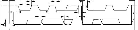
FUNCTIONAL BLOCK DIAGRAM
|
|
|
VDD |
GND |
|
|
|
POWER-ON |
|
|
AD5602/AD5612/AD5622 |
||
|
RESET |
|
|
|
|
|
|
DAC |
|
REF(+) |
OUTPUT |
VOUT |
|
|
|
8-/10-/12-BIT |
||||
|
REGISTER |
BUFFER |
||||
|
DAC |
|
||||
|
|
|
|
|
||
|
INPUT |
|
|
POWER-DOWN |
|
|
CONTROL |
|
|
CONTROL LOGIC |
RESISTOR |
||
|
LOGIC |
|
|
|
|
NETWORK |
ADDR |
SCL |
SDA |
|
|
|
05446-001 |
Figure 1.
Table 1. Related Devices
Part No. |
Description |
AD5601/AD5611/AD5621 |
2.7 V to 5.5 V, <100 µA, 8-, 10-, 12-bit |
|
nanoDAC with SPI® interface in tiny |
|
LFCSP and SC70 packages |
PRODUCT HIGHLIGHTS
1.Available in 6-lead LFCSP and SC70 packages.
2.Maximum 100 µA power consumption, single-supply operation. These parts operate from a single 2.7 V to 5.5 V supply, typically consuming 0.2 mW at 3 V and 0.4 mW at 5 V, making them ideal for battery-powered applications.
3.The on-chip output buffer amplifier allows the output of the DAC to swing rail-to-rail with a typical slew rate of 0.5 V/µs.
4.Reference derived from the power supply.
5.Standard, fast, and high speed mode I2C interface.
6.Designed for very low power consumption.
7.Power-down capability. When powered down, the DAC typically consumes <150 nA at 3 V.
8.Power-on reset and brownout detection.
One Technology Way, P.O. Box 9106, Norwood, MA 02062-9106, U.S.A. Tel: 781.329.4700 www.analog.com Fax: 781.461.3113 ©2005–2012 Analog Devices, Inc. All rights reserved.

AD5602/AD5612/AD5622 |
Data Sheet |
TABLE OF CONTENTS |
|
Features .............................................................................................. |
1 |
Applications....................................................................................... |
1 |
Functional Block Diagram .............................................................. |
1 |
General Description ......................................................................... |
1 |
Product Highlights ........................................................................... |
1 |
Revision History ............................................................................... |
2 |
Specifications..................................................................................... |
3 |
I2C Timing Specifications............................................................ |
4 |
Timing Diagram ........................................................................... |
5 |
Absolute Maximum Ratings............................................................ |
6 |
ESD Caution.................................................................................. |
6 |
Pin Configuration and Function Descriptions............................. |
7 |
Typical Performance Characteristics ............................................. |
8 |
Terminology .................................................................................... |
14 |
Theory of Operation ...................................................................... |
15 |
D/A Section................................................................................. |
15 |
REVISION HISTORY |
|
5/12—Rev. B to Rev. C |
|
Added 6-lead LFCSP Package........................................... |
Universal |
Changes to Product Title ................................................................. |
1 |
Changes to Ordering Guide .......................................................... |
23 |
3/06—Rev. A to Rev. B |
|
Changes to Table 2............................................................................ |
3 |
Updates to Outline Dimensions ................................................... |
22 |
Changes to Ordering Guide .......................................................... |
23 |
8/05—Rev. 0 to Rev. A |
|
Changes to Ordering Guide .......................................................... |
22 |
6/05—Revision 0: Initial Version |
|
Resistor String............................................................................. |
15 |
Output Amplifier........................................................................ |
15 |
Serial Interface ................................................................................ |
16 |
Input Register.............................................................................. |
16 |
Power-On Reset.......................................................................... |
17 |
Power-Down Modes .................................................................. |
17 |
Write Operation.......................................................................... |
18 |
Read Operation........................................................................... |
19 |
High Speed Mode....................................................................... |
20 |
Applications..................................................................................... |
21 |
Choosing a Reference as Power Supply................................... |
21 |
Bipolar Operation....................................................................... |
21 |
Power Supply Bypassing and Grounding................................ |
21 |
Outline Dimensions ....................................................................... |
22 |
Ordering Guide .......................................................................... |
23 |
Rev. C | Page 2 of 24

Data Sheet |
AD5602/AD5612/AD5622 |
SPECIFICATIONS
VDD = 2.7 V to 5.5 V, RL = 2 kΩ to GND, CL = 200 pF to GND; all specifications TMIN to TMAX, unless otherwise noted.
Table 2.
|
A, B, W, Y Versions1 |
|
|
||
Parameter |
Min |
Typ |
Max |
Unit |
Test Conditions/Comments |
STATIC PERFORMANCE |
|
|
|
|
DAC output unloaded |
Resolution |
|
|
|
Bits |
|
AD5602 |
8 |
|
|
|
|
AD5612 |
10 |
|
|
|
|
AD5622 |
12 |
|
|
|
|
Relative Accuracy2 |
|
|
|
|
|
AD5602 |
|
|
±0.5 |
LSB |
B, Y versions |
AD5612 |
|
|
±0.5 |
LSB |
B, Y versions |
|
|
|
±4 |
LSB |
A version |
AD5622 |
|
|
±2 |
LSB |
B, Y versions |
|
|
|
±6 |
LSB |
A, W versions |
Differential Nonlinearity2 |
|
|
±1 |
LSB |
Guaranteed monotonic by design |
Zero Code Error |
|
0.5 |
10 |
mV |
All 0s loaded to DAC register |
Offset Error |
|
±0.063 |
±10 |
mV |
|
Full-Scale Error |
|
0.5 |
|
mV |
All 1s loaded to DAC register |
Gain Error |
|
±0.0004 |
±0.037 |
% of FSR |
|
Zero Code Error Drift |
|
5 |
|
µV/°C |
|
Gain Temperature Coefficient |
|
2 |
|
ppm of FSR/°C |
|
OUTPUT CHARACTERISTICS3 |
|
|
|
|
|
Output Voltage Range |
0 |
|
VDD |
V |
|
Output Voltage Settling Time |
|
6 |
10 |
µs |
Code ¼ to ¾ |
Slew Rate |
|
0.5 |
|
V/µs |
|
Capacitive Load Stability |
|
470 |
|
pF |
RL = ∞ |
|
|
1000 |
|
pF |
RL = 2 kΩ |
Output Noise Spectral Density |
|
120 |
|
nV/Hz |
DAC code = midscale, 10 kHz |
Noise |
|
2 |
|
|
DAC code = midscale, 0.1 Hz to 10 Hz |
|
|
|
|
|
bandwidth |
Digital-to-Analog Glitch Impulse |
|
5 |
|
nV-s |
1 LSB change around major carry |
Digital Feedthrough |
|
0.2 |
|
nV-s |
|
DC Output Impedance |
|
0.5 |
|
Ω |
|
Short Circuit Current |
|
15 |
|
mA |
VDD = 3 V/5 V |
LOGIC INPUTS (SDA, SCL) |
|
|
|
|
|
IIN, Input Current |
|
|
±1 |
µA |
|
VINL, Input Low Voltage |
|
|
0.3 × VDD |
V |
|
VINH, Input High Voltage |
0.7 × VDD |
|
|
V |
|
CIN, Pin Capacitance |
|
2 |
|
pF |
|
VHYST, Input Hysteresis |
0.1 × VDD |
|
|
V |
|
LOGIC OUTPUTS (OPEN DRAIN) |
|
|
|
|
|
VOL, Output Low Voltage |
|
|
0.4 |
V |
ISINK = 3 mA |
|
|
|
0.6 |
V |
ISINK = 6 mA |
Floating-State Leakage Current |
|
|
±1 |
µA |
|
Floating-State Output Capacitance |
|
2 |
|
pF |
|
|
|
|
|
|
|
Rev. C | Page 3 of 24
AD5602/AD5612/AD5622 |
|
|
|
|
Data Sheet |
|
|
|
|
|
|
|
|
|
|
|
|
|
|
A, B, W, Y Versions1 |
|
|
|
Parameter |
Min |
Typ |
Max |
Unit |
Test Conditions/Comments |
|
|
|
|
|
|
POWER REQUIREMENTS |
|
|
|
|
|
VDD |
2.7 |
|
5.5 |
V |
|
IDD (Normal Mode) |
|
|
|
|
DAC active and excluding load current |
VDD = 4.5 V to 5.5 V |
|
75 |
100 |
µA |
VIH = VDD and VIL = GND |
VDD = 2.7 V to 3.6 V |
|
60 |
90 |
µA |
VIH = VDD and VIL = GND |
IDD (All Power-Down Modes) |
|
|
|
|
|
VDD = 4.5 V to 5.5 V |
|
0.3 |
1 |
µA |
VIH = VDD and VIL = GND |
VDD = 2.7 V to 3.6 V |
|
0.15 |
1 |
µA |
VIH = VDD and VIL = GND |
POWER EFFICIENCY |
|
|
|
|
|
IOUT/IDD |
|
96 |
|
% |
ILOAD = 2 mA, VDD = 5 V |
|
|
|
|
|
|
1Temperature ranges for A, B versions: −40°C to +125°C, typical at 25°C.
2Linearity calculated using a reduced code range 64 to 4032.
3Guaranteed by design and characterization, not production tested.
I2C TIMING SPECIFICATIONS
VDD = 2.7 V to 5.5 V; all specifications TMIN to TMAX, fSCL = 3.4 MHz, unless otherwise noted.1
Table 3.
|
|
Limit at TMIN, TMAX |
|
|
|
Parameter |
Conditions2 |
Min |
Max |
Unit |
Description |
fSCL3 |
Standard mode |
|
100 |
KHz |
Serial clock frequency |
|
Fast mode |
|
400 |
KHz |
|
|
High speed mode, CB = 100 pF |
|
3.4 |
MHz |
|
|
High speed mode, CB = 400 pF |
|
1.7 |
MHz |
|
t1 |
Standard mode |
4 |
|
µs |
tHIGH, SCL high time |
|
Fast mode |
0.6 |
|
µs |
|
|
High speed mode, CB = 100 pF |
60 |
|
ns |
|
|
High speed mode, CB = 400 pF |
120 |
|
ns |
|
t2 |
Standard mode |
4.7 |
|
µs |
tLOW, SCL low time |
|
Fast mode |
1.3 |
|
µs |
|
|
High speed mode, CB = 100 pF |
160 |
|
ns |
|
|
High speed mode, CB = 400 pF |
320 |
|
ns |
|
t3 |
Standard mode |
250 |
|
ns |
tSU;DAT, data setup time |
|
Fast mode |
100 |
|
ns |
|
|
High speed mode |
10 |
|
ns |
|
t4 |
Standard mode |
0 |
3.45 |
µs |
tHD;DAT, data hold time |
|
Fast mode |
0 |
0.9 |
µs |
|
|
High speed mode, CB = 100 pF |
0 |
70 |
ns |
|
|
High speed mode, CB = 400 pF |
0 |
150 |
ns |
|
t5 |
Standard mode |
4.7 |
|
µs |
tSU;STA, set-up time for a repeated start condition |
|
Fast mode |
0.6 |
|
µs |
|
|
High speed mode |
160 |
|
ns |
|
t6 |
Standard mode |
4 |
|
µs |
tHD;STA, hold time (repeated) start condition |
|
Fast mode |
0.6 |
|
µs |
|
|
High speed mode |
160 |
|
ns |
|
t7 |
Standard mode |
4.7 |
|
µs |
tBUF, bus free time between a stop and a start |
|
|
|
|
|
condition |
|
Fast mode |
1.3 |
|
µs |
|
Rev. C | Page 4 of 24
Data Sheet |
|
|
|
AD5602/AD5612/AD5622 |
|
|
|
|
|
|
|
|
|
|
|
|
|
|
|
Limit at TMIN, TMAX |
|
|
|
Parameter |
Conditions2 |
Min |
Max |
Unit |
Description |
t8 |
Standard mode |
4 |
|
µs |
tSU;STO, setup time for a stop condition |
|
Fast mode |
0.6 |
|
µs |
|
|
High speed mode |
160 |
|
ns |
|
t9 |
Standard mode |
|
1000 |
ns |
tRDA, rise time of SDA signal |
|
Fast mode |
|
300 |
ns |
|
|
High speed mode, CB = 100 pF |
10 |
80 |
ns |
|
|
High speed mode, CB = 400 pF |
20 |
160 |
ns |
|
t10 |
Standard mode |
|
300 |
ns |
tFDA, fall time of SDA signal |
|
Fast mode |
|
300 |
ns |
|
|
High speed mode, CB = 100 pF |
10 |
80 |
ns |
|
|
High speed mode, CB = 400 pF |
20 |
160 |
ns |
|
t11 |
Standard mode |
|
1000 |
ns |
tRCL, rise time of SCL signal |
|
Fast mode |
|
300 |
ns |
|
|
High speed mode, CB = 100 pF |
10 |
40 |
ns |
|
|
High speed mode, CB = 400 pF |
20 |
80 |
ns |
|
t11A |
Standard mode |
|
1000 |
ns |
tRCL1, rise time of SCL signal after a repeated start |
|
|
|
|
|
condition and after an acknowledge bit |
|
Fast mode |
|
300 |
ns |
|
|
High speed mode, CB = 100 pF |
10 |
80 |
ns |
|
|
High speed mode, CB = 400 pF |
20 |
160 |
ns |
|
t12 |
Standard mode |
|
300 |
ns |
tFCL, fall time of SCL signal |
|
Fast mode |
|
300 |
ns |
|
|
High speed mode, CB = 100 pF |
10 |
40 |
ns |
|
|
High speed mode, CB = 400 pF |
20 |
80 |
ns |
|
tSP4 |
Fast mode |
0 |
50 |
ns |
Pulse width of spike suppressed |
|
High speed mode |
0 |
10 |
ns |
|
|
|
|
|
|
|
1See Figure 2. High speed mode timing specification applies to the AD5602-1/AD5612-1/AD5622-1 only. Standard and fast mode timing specifications apply to the AD5602-1/AD5612-1/AD5622-1 and AD5602-2/AD5612-2/AD5622-2.
2CB refers to the capacitance on the bus line.
3The SDA and SCL timing is measured with the input filters enabled. Switching off the input filters improves the transfer rate but has a negative effect on EMC behavior of the part.
4Input filtering on the SCL and SDA inputs suppress noise spikes that are less than 50 ns for fast mode or 10 ns for high speed mode.
TIMING DIAGRAM
|
t11 |
t12 |
t6 |
SCL |
t2 |
|
|
|
|
|
|
|
t6 |
t1 |
t5 |
|
t4 |
t3 |
t10 |
SDA |
|
|
|
|
t7 |
|
|
P |
S |
|
S |
Figure 2. 2-Wire Serial Interface Timing Diagram
t8 

 t9
t9
P
05446-002
Rev. C | Page 5 of 24

AD5602/AD5612/AD5622 |
Data Sheet |
ABSOLUTE MAXIMUM RATINGS
TA = 25°C, unless otherwise noted.
Table 4.
Parameter |
Rating |
|
|
VDD to GND |
–0.3 V to + 7.0 V |
Digital Input Voltage to GND |
–0.3 V to VDD + 0.3 V |
VOUT to GND |
–0.3 V to VDD + 0.3 V |
Operating Temperature Range |
|
Extended Automotive (W, Y Versions) |
–40°C to +125°C |
Extended Industrial (A, B Versions) |
−40°C to +85°C |
Storage Temperature Range |
–65°C to +160°C |
Maximum Junction Temperature |
150°C |
SC70 Package |
|
θJA Thermal Impedance |
332°C/W |
θJC Thermal Impedance |
120°C/W |
LFCSP Package |
|
θJA Thermal Impedance |
95°C/W |
Lead Temperature, Soldering |
|
Vapor Phase (60 sec) |
215°C |
Infrared (15 sec) |
220°C |
ESD |
2.0 kV |
Stresses above those listed under Absolute Maximum Ratings may cause permanent damage to the device. This is a stress rating only; functional operation of the device at these or any other conditions above those indicated in the operational section of this specification is not implied. Exposure to absolute maximum rating conditions for extended periods may affect device reliability.
ESD CAUTION
ESD (electrostatic discharge) sensitive device. Electrostatic charges as high as 4000 V readily accumulate on the human body and test equipment and can discharge without detection. Although this product features proprietary ESD protection circuitry, permanent damage may occur on devices subjected to high energy electrostatic discharges. Therefore, proper ESD precautions are recommended to avoid performance degradation or loss of functionality.
Rev. C | Page 6 of 24
Data Sheet |
AD5602/AD5612/AD5622 |
PIN CONFIGURATION AND FUNCTION DESCRIPTIONS
ADDR |
|
|
|
VOUT |
|
1 |
AD5602/ |
6 |
|
||
|
|
|
|
||
|
|
AD5612/ |
|
|
|
SCL |
2 |
AD5622 |
5 |
GND |
|
|
|
TOP VIEW |
|
|
003- |
SDA |
|
(Not to Scale) |
|
VDD |
|
3 |
|
4 |
05446 |
||
|
|
|
|
|
Figure 3. SC70 Pin Configuration
ADDR |
1 |
AD5602/ |
6 |
SDA |
|
|
|
|
|
GND |
2 |
AD5612/ |
5 |
SCL |
AD5622 |
||||
|
|
TOP VIEW |
|
|
VOUT |
3 |
(Not to Scale) |
4 |
VDD |
|
NOTES
1. THE EXPOSED PAD SHOULD BE CONNECTED TO GROUND (GND).
Figure 4. LFCSP Pin Configuration
05446-051
Table 5. SC79 Pin Function Descriptions
Pin No. |
Mnemonic |
Description |
|
|
|
1 |
ADDR |
Three-State Address Input. Sets the two |
|
|
least significant bits (Bit A1, Bit A0) of |
|
|
the 7-bit slave address (see Table 7). |
2 |
SCL |
Serial Clock Line. This is used in |
|
|
conjunction with the SDA line to clock |
|
|
data into or out of the 16-bit input |
|
|
register. |
3 |
SDA |
Serial Data Line. This is used in |
|
|
conjunction with the SCL line to clock |
|
|
data into or out of the 16-bit input |
|
|
register. It is a bidirectional, open-drain |
|
|
data line that should be pulled to the |
|
|
supply with an external pull-up resistor. |
4 |
VDD |
Power Supply Input. These parts can be |
|
|
operated from 2.7 V to 5.5 V, and VDD |
|
|
should be decoupled to GND. |
5 |
GND |
Ground. The ground reference point for |
|
|
all circuitry on the part. |
6 |
VOUT |
Analog Output Voltage from the DAC. |
|
|
The output amplifier has rail-to-rail |
|
|
operation. |
|
|
|
Table 6. LFCSP Pin Function Descriptions
Pin No. |
Mnemonic |
Description |
|
|
|
1 |
ADDR |
Three-State Address Input. Sets the |
|
|
two least significant bits (Bit A1, Bit A0) |
|
|
of the 7-bit slave address (see Table 7). |
2 |
GND |
Ground. The ground reference point for |
|
|
all circuitry on the part. |
3 |
VOUT |
Analog Output Voltage from the DAC. |
|
|
The output amplifier has rail-to-rail |
|
|
operation. |
4 |
VDD |
Power Supply Input. These parts can be |
|
|
operated from 2.7 V to 5.5 V, and VDD |
|
|
should be decoupled to GND. |
5 |
SCL |
Serial Clock Line. This is used in |
|
|
conjunction with the SDA line to clock |
|
|
data into or out of the 16-bit input |
|
|
register. |
6 |
SDA |
Serial Data Line. This is used in |
|
|
conjunction with the SCL line to clock |
|
|
data into or out of the 16-bit input |
|
|
register. It is a bidirectional, open-drain |
|
|
data line that should be pulled to the |
|
|
supply with an external pull-up resistor. |
|
EPAD |
Exposed Pad. The exposed pad should |
|
|
be connected to ground (GND). |
Rev. C | Page 7 of 24

AD5602/AD5612/AD5622 |
Data Sheet |
TYPICAL PERFORMANCE CHARACTERISTICS
|
1.0 |
VDD = 5V |
|
|
|
|
|
|
|
|
|
|
|
|
|
|
|
|
|
|
|
|
0.8 |
TA = 25°C |
|
|
|
|
|
|
|
|
|
0.6 |
|
|
|
|
|
|
|
|
|
(LSB) |
0.4 |
|
|
|
|
|
|
|
|
|
0.2 |
|
|
|
|
|
|
|
|
|
|
ERROR |
0 |
|
|
|
|
|
|
|
|
|
–0.2 |
|
|
|
|
|
|
|
|
|
|
INL |
|
|
|
|
|
|
|
|
|
|
–0.4 |
|
|
|
|
|
|
|
|
|
|
|
|
|
|
|
|
|
|
|
|
|
|
–0.6 |
|
|
|
|
|
|
|
|
|
|
–0.8 |
|
|
|
|
|
|
|
|
|
|
–1.0 |
|
|
|
|
|
|
|
|
-004 |
|
0 |
500 |
1000 |
1500 |
2000 |
2500 |
3000 |
3500 |
4000 |
|
|
05446 |
|||||||||
|
|
|
|
|
DAC CODE |
|
|
|
||
Figure 5. Typical AD5622 Integral Nonlinearity Error
|
0.15 |
|
|
|
|
|
|
|
|
|
|
|
|
|
|
|
|
|
|
|
|
|
|
|
|
|
|
|
|
|
|
|
|
|
|
|
|
|
|
|
|
|
|
|
VDD = |
5V |
|
|
|
|
|
|
|
|
|
|
|
|
|
|
|
|
|
0.10 |
|
TA = 25°C |
|
|
|
|
|
|
|
|
|
|
|
|
|
|
|
|
|
|
|
|
|
|
|
|
|
|
|
|
|
|
|
|
|
|
|
|
|
|
(LSB) |
0.05 |
|
|
|
|
|
|
|
|
|
|
|
|
|
|
|
|
|
|
|
|
|
|
|
|
|
|
|
|
|
|
|
|
|
|
|
|
|
|
||
0 |
|
|
|
|
|
|
|
|
|
|
|
|
|
|
|
|
|
|
|
|
ERROR |
|
|
|
|
|
|
|
|
|
|
|
|
|
|
|
|
|
|
|
|
–0.05 |
|
|
|
|
|
|
|
|
|
|
|
|
|
|
|
|
|
|
|
|
|
|
|
|
|
|
|
|
|
|
|
|
|
|
|
|
|
|
|
||
DNL |
–0.10 |
|
|
|
|
|
|
|
|
|
|
|
|
|
|
|
|
|
|
|
|
|
|
|
|
|
|
|
|
|
|
|
|
|
|
|
|
|
|
|
|
|
|
|
|
|
|
|
|
|
|
|
|
|
|
|
|
|
|
|
|
|
|
–0.15 |
|
|
|
|
|
|
|
|
|
|
|
|
|
|
|
|
|
|
|
|
|
|
|
|
|
|
|
|
|
|
|
|
|
|
|
|
|
|
|
|
|
–0.20 |
|
|
|
|
|
|
|
|
|
|
|
|
|
|
|
|
|
|
-005 |
|
0 |
500 |
1000 |
1500 |
2000 |
2500 |
3000 |
3500 |
4000 |
|||||||||||
|
05446 |
|||||||||||||||||||
|
|
|
|
|
|
|
|
|
DAC CODE |
|
|
|
|
|
|
|
||||
Figure 6. Typical AD5622 Differential Nonlinearity Error
|
0.25 |
VDD = 5V |
|
|
|
|
|
|
|
|
|
|
|
|
|
|
0.20 |
TA = 25°C |
|
|
|
|
|
|
0.15 |
|
|
|
|
|
|
(LSB) |
0.10 |
|
|
|
|
|
|
0.05 |
|
|
|
|
|
|
|
ERROR |
0 |
|
|
|
|
|
|
–0.05 |
|
|
|
|
|
|
|
INL |
|
|
|
|
|
|
|
–0.10 |
|
|
|
|
|
|
|
|
|
|
|
|
|
|
|
|
–0.15 |
|
|
|
|
|
|
|
–0.20 |
|
|
|
|
|
|
|
–0.25 |
|
|
|
|
|
-047 |
|
0 |
200 |
400 |
600 |
800 |
1000 |
|
|
05446 |
||||||
|
|
|
DAC CODE |
|
|
||
Figure 7. Typical AD5612 Integral Nonlinearity Error
|
0.05 |
VDD = 5V |
|
|
|
|
|
|
|
|
|
|
|
|
|
|
0.04 |
TA = 25°C |
|
|
|
|
|
|
0.03 |
|
|
|
|
|
|
(LSB) |
0.02 |
|
|
|
|
|
|
0.01 |
|
|
|
|
|
|
|
ERROR |
0 |
|
|
|
|
|
|
–0.01 |
|
|
|
|
|
|
|
DNL |
|
|
|
|
|
|
|
–0.02 |
|
|
|
|
|
|
|
|
|
|
|
|
|
|
|
|
–0.03 |
|
|
|
|
|
|
|
–0.04 |
|
|
|
|
|
|
|
–0.05 |
|
|
|
|
|
-048 |
|
0 |
200 |
400 |
600 |
800 |
1000 |
|
|
05446 |
||||||
|
|
|
DAC CODE |
|
|
||
Figure 8. Typical AD5612 Differential Nonlinearity Error
|
0.06 |
VDD = 5V |
|
|
|
|
|
|
|
|
|
|
|
|
|
|
|
TA = 25°C |
|
|
|
|
|
|
0.04 |
|
|
|
|
|
|
(LSB) |
0.02 |
|
|
|
|
|
|
|
|
|
|
|
|
|
|
INL ERROR |
0 |
|
|
|
|
|
|
–0.02 |
|
|
|
|
|
|
|
|
|
|
|
|
|
|
|
|
–0.04 |
|
|
|
|
|
|
|
–0.06 |
|
|
|
|
|
-049 |
|
0 |
50 |
100 |
150 |
200 |
250 |
|
|
05446 |
||||||
|
|
|
DAC CODE |
|
|
||
Figure 9. Typical AD5602 Integral Nonlinearity Error
|
0.015 |
VDD = 5V |
|
|
|
|
|
|
|
|
|
|
|
|
|
|
|
TA = 25°C |
|
|
|
|
|
|
0.010 |
|
|
|
|
|
|
(LSB) |
0.005 |
|
|
|
|
|
|
|
|
|
|
|
|
|
|
DNL ERROR |
0 |
|
|
|
|
|
|
–0.005 |
|
|
|
|
|
|
|
|
|
|
|
|
|
|
|
|
–0.010 |
|
|
|
|
|
|
|
–0.015 |
|
|
|
|
|
-050 |
|
0 |
50 |
100 |
150 |
200 |
250 |
|
|
05446 |
||||||
|
|
|
DAC CODE |
|
|
||
Figure 10. Typical AD5602 Differential Nonlinearity Error
Rev. C | Page 8 of 24
Loading...