


 Loading...
Quad, 12-/14-/16-Bit nanoDACs with 5 ppm/°C On-Chip Reference, I2C Interface
AD5625R/AD5645R/AD5665R, AD5625/AD5665
FEATURES
Low power, smallest pin-compatible, quad nanoDACs AD5625R/AD5645R/AD5665R
12-/14-/16-bit nanoDACs
On-chip, 2.5 V, 5 ppm/°C reference in TSSOP On-chip, 2.5 V, 10 ppm/°C reference in LFCSP On-chip, 1.25 V, 10 ppm/°C reference in LFCSP
AD5625/AD5665 12-/16-bit nanoDACs External reference only
3 mm × 3 mm 10-lead LFCSP and 14-lead TSSOP 2.7 V to 5.5 V power supply
Guaranteed monotonic by design Power-on reset to zero scale/midscale Per channel power-down
Hardware LDAC and CLR functions
I2C-compatible serial interface supports standard (100 kHz), fast (400 kHz), and high speed (3.4 MHz) modes
APPLICATIONS
Process control
Data acquisition systems
Portable battery-powered instruments
Digital gain and offset adjustment
Programmable voltage and current sources
Programmable attenuators
GENERAL DESCRIPTION
The AD5625R/AD5645R/AD5665R and AD5625/AD5665 members of the nanoDAC® family are low power, quad, 12-/ 14-/16-bit, buffered voltage-out DACs with/without an on-chip reference. All devices operate from a single 2.7 V to 5.5 V supply, are guaranteed monotonic by design, and have an I2C-compatible serial interface.
|
FUNCTIONAL BLOCK DIAGRAMS |
|
||||
|
|
VDD |
GND |
VREFIN/VREFOUT |
|
|
|
AD5625R/AD5645R/AD5665R |
1.25V/2.5V REF |
|
|||
|
|
|
|
BUFFER |
|
|
ADDR1 |
|
INPUT |
DAC |
STRING |
VOUTA |
|
|
REGISTER |
REGISTER |
DAC A |
|||
|
|
|
|
BUFFER |
|
|
ADDR2 |
INTERFACE LOGIC |
INPUT |
DAC |
STRING |
VOUTB |
|
|
REGISTER |
REGISTER |
DAC B |
|||
|
INPUT |
DAC |
STRING |
VOUTC |
||
SCL |
|
|
|
BUFFER |
|
|
|
|
|
|
|
||
|
|
REGISTER |
REGISTER |
DAC C |
|
|
SDA |
|
|
|
BUFFER |
|
|
|
|
INPUT |
DAC |
STRING |
VOUTD |
|
|
|
REGISTER |
REGISTER |
DAC D |
||
|
|
|
||||
|
|
POWER-ON RESET |
POWER-DOWN LOGIC |
|
||
NOTES |
LDAC CLR |
POR |
|
|
-001 |
|
|
|
|
|
|||
1. THE FOLLOWING PINS ARE AVAILABLE ONLY ON 14-LEAD PACKAGE: |
||||||
06341 |
||||||
ADDR2, LDAC, CLR, POR. |
|
|
||||
|
Figure 1. AD5625R/AD5645R/AD5665R |
|
||||
|
|
VDD |
GND |
VREFIN |
|
|
|
AD5625/AD5665 |
|
|
|
||
|
|
|
|
BUFFER |
|
|
ADDR1 |
|
INPUT |
DAC |
STRING |
VOUTA |
|
|
REGISTER |
REGISTER |
DAC A |
|||
|
|
|
|
BUFFER |
|
|
ADDR2 |
INTERFACE LOGIC |
INPUT |
DAC |
STRING |
VOUTB |
|
|
REGISTER |
REGISTER |
DAC B |
|||
|
REGISTER |
REGISTER |
DAC C |
VOUTC |
||
SCL |
|
|
|
BUFFER |
|
|
|
INPUT |
DAC |
STRING |
|
||
|
|
|
||||
SDA |
|
|
|
BUFFER |
|
|
|
|
INPUT |
DAC |
STRING |
VOUTD |
|
|
|
REGISTER |
REGISTER |
DAC D |
||
|
|
POWER-ON RESET |
POWER-DOWN LOGIC |
|
||
NOTES |
LDAC CLR |
POR |
|
|
002- |
|
|
|
|
|
|||
1. THE FOLLOWING PINS ARE AVAILABLE ONLY ON 14-LEAD PACKAGE: |
||||||
06341 |
||||||
ADDR2, LDAC, CLR, POR. |
|
|
||||
The AD5625R/AD5645R/AD5665R have an on-chip reference. The LFCSP versions of the AD56x5R have a 1.25 V or 2.5 V,
10 ppm/°C reference, giving a full-scale output range of 2.5 V or 5 V; the TSSOP versions of the AD56x5R have a 2.5 V, 5 ppm/°C reference, giving a full-scale output range of 5 V. The on-chip reference is off at power-up, allowing the use of an external reference. The internal reference is enabled via a software write. The AD5625/AD5665 require an external reference voltage to set the output range of the DAC.
The part incorporates a power-on reset circuit that ensures that the DAC output powers up to 0 V (POR = GND) or midscale (POR = VDD) and remains there until a valid write occurs. The on-chip precision output amplifier enables rail-to-rail output swing.
Rev. B
Information furnished by Analog Devices is believed to be accurate and reliable. However, no responsibilityisassumedbyAnalogDevicesforitsuse,norforanyinfringementsofpatentsorother rightsofthirdpartiesthatmayresultfromitsuse.Specificationssubjecttochangewithoutnotice.No license is granted by implication or otherwise under any patent or patent rights of Analog Devices. Trademarksandregisteredtrademarksarethepropertyoftheirrespectiveowners.
Figure 2. AD5625/AD5665
The AD56x5R/AD56x5 use a 2-wire I2C-compatible serial interface that operates in standard (100 kHz), fast (400 kHz), and high speed (3.4 MHz) modes.
Table 1. Related Devices
Part No. |
Description |
|
|
AD5025/AD5045/AD5065 |
Dual 12-/14-/16-bit DACs |
AD5624R/AD5644R/AD5664R, |
Quad SPI 12-/14-/16-bit DACs, |
AD5624/AD5664 |
with/without internal reference |
AD5627R/AD5647R/AD5667R, |
Dual I2C 12-/14-/16-bit DACs, |
AD5627/AD5667 |
with/without internal reference |
AD5666 |
Quad SPI 16-bit DAC with |
|
internal reference |
One Technology Way, P.O. Box 9106, Norwood, MA 02062-9106, U.S.A. Tel: 781.329.4700 www.analog.com Fax: 781.461.3113 ©2007-2009 Analog Devices, Inc. All rights reserved.

AD5625R/AD5645R/AD5665R, AD5625/AD5665
TABLE OF CONTENTS |
|
Features .............................................................................................. |
1 |
Applications....................................................................................... |
1 |
General Description ......................................................................... |
1 |
Functional Block Diagrams............................................................. |
1 |
Revision History ............................................................................... |
2 |
Specifications..................................................................................... |
3 |
Specifications—AD5665R/AD5645R/AD5625R ..................... |
3 |
Specifications—AD5665/AD5625 ............................................. |
5 |
AC Characteristics........................................................................ |
7 |
I2C Timing Specifications............................................................ |
8 |
Absolute Maximum Ratings.......................................................... |
10 |
ESD Caution................................................................................ |
10 |
Pin Configurations and Function Descriptions ......................... |
11 |
Typical Performance Characteristics ........................................... |
12 |
Terminology .................................................................................... |
20 |
Theory of Operation ...................................................................... |
22 |
Digital-to-Analog Converter (DAC) ....................................... |
22 |
Resistor String............................................................................. |
22 |
Output Amplifier........................................................................ |
22 |
Internal Reference ...................................................................... |
22 |
REVISION HISTORY |
|
12/09—Rev. A to Rev. B |
|
Changes to Features Section, General Description Section, |
|
and Table 1......................................................................................... |
1 |
Changes to Table 2............................................................................ |
3 |
Changes to Internal Reference Section........................................ |
22 |
Updated Outline Dimensions ....................................................... |
32 |
Changes to Ordering Guide .......................................................... |
33 |
6/09—Rev. 0 to Rev. A |
|
Changes to Features and General Description Sections.............. |
1 |
Changes to Table 2............................................................................ |
3 |
Changes to Table 3............................................................................ |
5 |
Changes to Digital-to-Analog Converter (DAC) Section, Added |
|
Figure 54 and Figure 55, Renumbered Subsequent Figures ..... |
22 |
Changes to Ordering Guide .......................................................... |
33 |
3/07—Revision 0: Initial Version |
|
External Reference ..................................................................... |
23 |
Serial Interface ............................................................................ |
23 |
Write Operation.......................................................................... |
23 |
Read Operation........................................................................... |
23 |
High Speed Mode....................................................................... |
25 |
Input Shift Register .................................................................... |
25 |
Multiple Byte Operation............................................................ |
25 |
Broadcast Mode.......................................................................... |
27 |
LDAC Function .......................................................................... |
27 |
Power-Down Modes .................................................................. |
29 |
Power-On Reset and Software Reset ....................................... |
30 |
Internal Reference Setup (R Versions) .................................... |
30 |
Applications Information .............................................................. |
31 |
Using a Reference as a Power Supply for the |
|
AD56x5R/AD56x5..................................................................... |
31 |
Bipolar Operation Using the AD56x5R/AD56x5 .................. |
31 |
Power Supply Bypassing and Grounding................................ |
31 |
Outline Dimensions ....................................................................... |
32 |
Ordering Guide .......................................................................... |
33 |
Rev. B | Page 2 of 36

AD5625R/AD5645R/AD5665R, AD5625/AD5665
SPECIFICATIONS
SPECIFICATIONS—AD5665R/AD5645R/AD5625R
VDD = 2.7 V to 5.5 V; RL = 2 kΩ to GND; CL = 200 pF to GND; VREFIN = VDD; all specifications TMIN to TMAX, unless otherwise noted.
Table 2.
|
A Grade |
|
B Grade |
|
|
|
Parameter |
Min Typ |
Max |
Min Typ |
Max |
Unit |
Test Conditions/Comments1 |
STATIC PERFORMANCE2 |
|
|
|
|
|
|
AD5665R |
|
|
|
|
|
|
Resolution |
|
|
16 |
|
Bits |
|
Relative Accuracy |
|
|
±8 |
±16 |
LSB |
|
Differential Nonlinearity |
|
|
|
±1 |
LSB |
Guaranteed monotonic by design |
AD5645R |
|
|
|
|
|
|
Resolution |
|
|
14 |
|
Bits |
|
Relative Accuracy |
|
|
±2 |
±4 |
LSB |
|
Differential Nonlinearity |
|
|
|
±0.5 |
LSB |
Guaranteed monotonic by design |
AD5625R |
|
|
|
|
|
|
Resolution |
12 |
|
12 |
|
Bits |
|
Relative Accuracy |
±1 |
±4 |
±0.5 |
±1 |
LSB |
|
Differential Nonlinearity |
|
±1 |
|
±0.25 |
LSB |
Guaranteed monotonic by design |
Zero-Code Error |
2 |
10 |
2 |
10 |
mV |
All 0s loaded to DAC register |
Offset Error |
±1 |
±10 |
±1 |
±10 |
mV |
|
Full-Scale Error |
−0.1 |
±0.5 |
−0.1 |
±0.5 |
% FSR |
All 1s loaded to DAC register |
Gain Error |
±0.1 |
±1.25 |
±0.1 |
±1 |
% FSR |
|
Zero-Code Error Drift |
±2 |
|
±2 |
|
μV/°C |
|
Gain Temperature Coefficient |
±2.5 |
|
±2.5 |
|
ppm |
Of FSR/°C |
DC Power Supply Rejection |
−100 |
|
−100 |
|
dB |
DAC code = midscale; VDD = 5 V ± 10% |
Ratio |
|
|
|
|
|
|
DC Crosstalk (External |
15 |
|
15 |
|
μV |
Due to full-scale output change, |
Reference) |
|
|
|
|
|
RL = 2 kΩ to GND or VDD |
|
10 |
|
10 |
|
μV/mA |
Due to load current change |
|
8 |
|
8 |
|
μV |
Due to powering down (per channel) |
DC Crosstalk (Internal |
25 |
|
25 |
|
μV |
Due to full-scale output change, |
Reference) |
|
|
|
|
|
RL = 2 kΩ to GND or VDD |
|
20 |
|
20 |
|
μV/mA |
Due to load current change |
|
10 |
|
10 |
|
μV |
Due to powering down (per channel) |
|
|
|
|
|
|
|
OUTPUT CHARACTERISTICS3 |
|
|
|
|
|
|
Output Voltage Range |
0 |
VDD |
0 |
VDD |
V |
Internal reference disabled |
|
0 |
2 × |
|
2 × |
|
Internal reference enabled |
|
|
VREF |
|
VREF |
|
|
Capacitive Load Stability |
2 |
|
2 |
|
nF |
RL = ∞ |
|
10 |
|
10 |
|
nF |
RL = 2 kΩ |
DC Output Impedance |
0.5 |
|
0.5 |
|
Ω |
|
Short-Circuit Current |
30 |
|
30 |
|
mA |
VDD = 5 V |
Power-Up Time |
4 |
|
4 |
|
μs |
Coming out of power-down mode; |
|
|
|
|
|
|
VDD = 5 V |
REFERENCE INPUTS |
|
|
|
|
|
|
Reference Current |
210 |
260 |
210 |
260 |
μA |
VREF = VDD = 5.5 V |
Reference Input Range |
0.75 |
VDD |
0.75 |
VDD |
V |
|
Reference Input Impedance |
26 |
|
26 |
|
kΩ |
|
REFERENCE OUTPUT (1.25 V) |
|
|
|
|
|
|
Output Voltage |
1.247 |
1.253 |
1.247 |
1.253 |
V |
At ambient |
Reference TC3 |
±10 |
|
±10 |
|
ppm/°C |
|
Output Impedance |
7.5 |
|
7.5 |
|
kΩ |
|
|
|
|
|
|
|
|
Rev. B | Page 3 of 36

AD5625R/AD5645R/AD5665R, AD5625/AD5665
|
|
|
|
|
A Grade |
B Grade |
|
||
Parameter |
Min Typ |
Max |
Min Typ |
Max |
Unit |
||||
|
|
|
|
|
|
|
|
|
|
REFERENCE OUTPUT (2.5 V) |
|
|
|
|
|
||||
|
Output Voltage |
2.495 |
2.505 |
2.495 |
2.505 |
V |
|||
|
Reference TC3 |
±10 |
|
±5 |
±10 |
ppm/°C |
|||
|
Output Impedance |
7.5 |
|
7.5 |
|
kΩ |
|||
LOGIC INPUTS (ADDRx, |
|
|
|
|
|
|
|
||
CLR, |
|
|
|
|
|
|
|||
|
LDAC, |
POR)3 |
|
|
|
|
|
||
|
IIN, Input Current |
|
±1 |
|
±1 |
μA |
|||
|
VINL, Input Low Voltage |
|
0.15 × VDD |
|
0.15 × VDD |
V |
|||
|
VINH, Input High Voltage |
0.85 × VDD |
|
0.85 × VDD |
|
V |
|||
|
CIN, Pin Capacitance |
2 |
|
2 |
|
pF |
|||
|
VHYST, Input Hysteresis |
0.1 × VDD |
|
0.1 × VDD |
|
V |
|||
|
|
|
|
|
|
||||
LOGIC INPUTS (SDA, SCL)3 |
|
|
|
|
|
||||
|
IIN, Input Current |
|
±1 |
|
±1 |
μA |
|||
|
VINL, Input Low Voltage |
|
0.3 × VDD |
|
0.3 × VDD |
V |
|||
|
VINH, Input High Voltage |
0.7 × VDD |
|
0.7 × VDD |
|
V |
|||
|
CIN, Pin Capacitance |
2 |
|
2 |
|
pF |
|||
|
VHYST, Input Hysteresis |
0.1 × VDD |
|
0.1 × VDD |
|
V |
|||
|
|
|
|
|
0.05 × VDD |
|
0.05 × VDD |
|
V |
LOGIC OUTPUTS (SDA)3 |
|
|
|
|
|
||||
|
VOL, Output Low Voltage |
|
0.4 |
|
0.4 |
V |
|||
|
|
|
|
|
|
0.6 |
|
0.6 |
V |
Floating-State Leakage |
|
±1 |
|
±1 |
μA |
||||
|
Current |
|
|
|
|
|
|||
Floating-State Output |
2 |
|
2 |
|
pF |
||||
|
Capacitance |
|
|
|
|
|
|||
POWER REQUIREMENTS |
|
|
|
|
|
||||
|
VDD |
2.7 |
5.5 |
2.7 |
5.5 |
V |
|||
|
IDD (Normal Mode)4 |
|
|
|
|
|
|||
|
VDD = 4.5 V to 5.5 V |
1.0 |
1.16 |
1.0 |
1.16 |
mA |
|||
|
VDD = 2.7 V to 3.6 V |
0.9 |
1.05 |
0.9 |
1.05 |
mA |
|||
|
VDD = 4.5 V to 5.5 V |
1.9 |
2.14 |
1.9 |
2.14 |
mA |
|||
|
VDD = 2.7 V to 3.6 V |
1.4 |
1.59 |
1.4 |
1.59 |
mA |
|||
|
IDD (All Power-Down Modes)5 |
|
|
|
|
|
|||
|
VDD = 2.7 V to 5.5 V |
0.48 |
1 |
0.48 |
1 |
μA |
|||
|
VDD = 3.6 V to 5.5 V |
0.48 |
1 |
0.48 |
1 |
μA |
|||
Test Conditions/Comments1
VDD = 4.5 V to 5.5 V At ambient
High speed mode
Fast mode
ISINK = 3 mA
ISINK = 6 mA
VIH = VDD, VIL = GND, full-scale loaded Internal reference off
Internal reference off Internal reference on Internal reference on
VIH = VDD, VIL = GND (LFCSP) VIH = VDD, VIL = GND (TSSOP)
1 Temperature range of A and B grades is −40°C to +105°C.
2 Linearity calculated using a reduced code range: AD5665R (Code 512 to Code 65,024), AD5645R (Code 128 to Code 16,256), AD5625R (Code 32 to Code 4064). Output unloaded.
3 Guaranteed by design and characterization; not production tested.
4 Interface inactive. All DACs active. DAC outputs unloaded.
5 All DACs powered down. Power-down function is not available on 14-lead TSSOP parts when the part is powered with VDD < 3.6 V.
Rev. B | Page 4 of 36

AD5625R/AD5645R/AD5665R, AD5625/AD5665
SPECIFICATIONS—AD5665/AD5625
VDD = 2.7 V to 5.5 V; RL = 2 kΩ to GND; CL = 200 pF to GND; VREFIN = VDD; all specifications TMIN to TMAX, unless otherwise noted.
Table 3.
|
|
|
|
|
|
B Grade |
|
|
|
Parameter |
Min |
Typ |
Max |
Unit |
Test Conditions/Comments1 |
||||
STATIC PERFORMANCE2 |
|
|
|
|
|
||||
AD5665 |
|
|
|
|
|
||||
Resolution |
16 |
|
|
Bits |
|
||||
Relative Accuracy |
|
±8 |
±16 |
LSB |
|
||||
Differential Nonlinearity |
|
|
±1 |
LSB |
Guaranteed monotonic by design |
||||
AD5625 |
|
|
|
|
|
||||
Resolution |
12 |
|
|
Bits |
|
||||
Relative Accuracy |
|
±0.5 |
±1 |
LSB |
|
||||
Differential Nonlinearity |
|
|
±0.25 |
LSB |
Guaranteed monotonic by design |
||||
Zero-Code Error |
|
2 |
10 |
mV |
All 0s loaded to DAC register |
||||
Offset Error |
|
±1 |
±10 |
mV |
|
||||
Full-Scale Error |
|
−0.1 |
±0.5 |
% FSR |
All 1s loaded to DAC register |
||||
Gain Error |
|
±0.1 |
±1 |
% FSR |
|
||||
Zero-Code Error Drift |
|
±2 |
|
μV/°C |
|
||||
Gain Temperature Coefficient |
|
±2.5 |
|
ppm |
Of FSR/°C |
||||
DC Power Supply Rejection Ratio |
|
−100 |
|
dB |
DAC code = midscale; VDD = 5 V ± 10% |
||||
DC Crosstalk (External Reference) |
|
15 |
|
μV |
Due to full-scale output change, |
||||
|
|
|
|
|
|
|
|
|
RL = 2 kΩ to GND or VDD |
|
|
|
|
|
|
10 |
|
μV/mA |
Due to load current change |
|
|
|
|
|
|
8 |
|
μV |
Due to powering down (per channel) |
DC Crosstalk (Internal Reference) |
|
25 |
|
μV |
Due to full-scale output change, |
||||
|
|
|
|
|
|
|
|
|
RL = 2 kΩ to GND or VDD |
|
|
|
|
|
|
20 |
|
μV/mA |
Due to load current change |
|
|
|
|
|
|
10 |
|
μV |
Due to powering down (per channel) |
|
|
|
|
|
|
|
|
|
|
OUTPUT CHARACTERISTICS3 |
|
|
|
|
|
||||
Output Voltage Range |
0 |
|
VDD |
V |
|
||||
Capacitive Load Stability |
|
2 |
|
nF |
RL = ∞ |
||||
|
|
|
|
|
|
10 |
|
nF |
RL = 2 kΩ |
DC Output Impedance |
|
0.5 |
|
Ω |
|
||||
Short-Circuit Current |
|
30 |
|
mA |
VDD = 5 V |
||||
Power-Up Time |
|
4 |
|
μs |
Coming out of power-down mode; VDD = 5 V |
||||
REFERENCE INPUTS |
|
|
|
|
|
||||
Reference Current |
|
210 |
260 |
μA |
VREF = VDD = 5.5 V |
||||
Reference Input Range |
0.75 |
|
VDD |
V |
|
||||
Reference Input Impedance |
|
26 |
|
kΩ |
|
||||
LOGIC INPUTS (ADDRx, |
|
|
|
POR)3 |
|
|
|
|
|
CLR, |
|
LDAC, |
|
|
|
|
|
||
IIN, Input Current |
|
|
±1 |
μA |
|
||||
VINL, Input Low Voltage |
|
|
0.15 × VDD |
V |
|
||||
VINH, Input High Voltage |
0.85 × VDD |
|
|
V |
|
||||
CIN, Pin Capacitance |
|
2 |
|
pF |
|
||||
VHYST, Input Hysteresis |
0.1 × VDD |
|
|
V |
|
||||
|
|
|
|
|
|
||||
LOGIC INPUTS (SDA, SCL)3 |
|
|
|
|
|
||||
IIN, Input Current |
|
|
±1 |
μA |
|
||||
VINL, Input Low Voltage |
|
|
0.3 × VDD |
V |
|
||||
VINH, Input High Voltage |
0.7 × VDD |
|
|
V |
|
||||
CIN, Pin Capacitance |
|
2 |
|
pF |
|
||||
VHYST, Input Hysteresis |
0.1 × VDD |
|
|
V |
High speed mode |
||||
|
|
|
|
|
0.05 × VDD |
|
|
V |
Fast mode |
|
|
|
|
|
|
|
|
|
|
Rev. B | Page 5 of 36

AD5625R/AD5645R/AD5665R, AD5625/AD5665
|
|
B Grade |
|
|
|
Parameter |
Min |
Typ |
Max |
Unit |
Test Conditions/Comments1 |
LOGIC OUTPUTS (SDA)3 |
|
|
|
|
|
VOL, Output Low Voltage |
|
|
0.4 |
V |
ISINK = 3 mA |
|
|
|
0.6 |
V |
ISINK = 6 mA |
Floating-State Leakage Current |
|
|
±1 |
μA |
|
Floating-State Output Capacitance |
|
2 |
|
pF |
|
|
|
|
|
|
|
POWER REQUIREMENTS |
|
|
|
|
|
VDD |
2.7 |
|
5.5 |
V |
|
IDD (Normal Mode)4 |
|
|
|
|
VIH = VDD, VIL = GND, full-scale loaded |
VDD = 4.5 V to 5.5 V |
|
1.0 |
1.16 |
mA |
|
VDD = 2.7 V to 3.6 V |
|
0.9 |
1.05 |
mA |
|
IDD (All Power-Down Modes)5 |
|
|
|
|
|
VDD = 2.7 V to 5.5 V |
|
0.48 |
1 |
μA |
VIH = VDD, VIL = GND (LFCSP) |
VDD = 3.6 V to 5.5 V |
|
0.48 |
1 |
μA |
VIH = VDD, VIL = GND (TSSOP) |
1 Temperature range of B grade is −40°C to +105°C.
2 Linearity calculated using a reduced code range: AD5665 (Code 512 to Code 65,024), AD5625 (Code 32 to Code 4064). Output unloaded. 3 Guaranteed by design and characterization; not production tested.
4 Interface inactive. All DACs active. DAC outputs unloaded.
5 All DACs powered down. Power-down function is not available on 14-lead TSSOP parts when the part is powered with VDD < 3.6 V.
Rev. B | Page 6 of 36

AD5625R/AD5645R/AD5665R, AD5625/AD5665
AC CHARACTERISTICS
VDD = 2.7 V to 5.5 V; RL = 2 kΩ to GND; CL = 200 pF to GND; VREFIN = VDD; all specifications TMIN to TMAX, unless otherwise noted.
Table 4.
Parameter1,2 |
Min |
Typ |
Max |
Unit |
Output Voltage Settling Time |
|
|
|
|
AD5625R/AD5625 |
|
3 |
4.5 |
μs |
AD5645R |
|
3.5 |
5 |
μs |
AD5665R/AD5665 |
|
4 |
7 |
μs |
Slew Rate |
|
1.8 |
|
V/μs |
Digital-to-Analog Glitch Impulse |
|
|
|
|
|
|
15 |
|
nV-s |
|
|
5 |
|
nV-s |
Digital Feedthrough |
|
0.1 |
|
nV-s |
Reference Feedthrough |
|
−90 |
|
dB |
Digital Crosstalk |
|
0.1 |
|
nV-s |
Analog Crosstalk |
|
1 |
|
nV-s |
|
|
4 |
|
nV-s |
DAC-to-DAC Crosstalk |
|
1 |
|
nV-s |
|
|
4 |
|
nV-s |
Multiplying Bandwidth |
|
340 |
|
kHz |
Total Harmonic Distortion |
|
−80 |
|
dB |
Output Noise Spectral Density |
|
120 |
|
nV/√Hz |
|
|
100 |
|
nV/√Hz |
Output Noise |
|
15 |
|
μV p-p |
|
|
|
|
|
1 Guaranteed by design and characterization; not production tested.
2 See the Terminology section.
3 Temperature range is −40°C to +105°C, typical @ 25°C.
Test Conditions/Comments3
¼to ¾ scale settling to ±0.5 LSB
¼to ¾ scale settling to ±0.5 LSB
¼to ¾ scale settling to ±2 LSB
1 LSB change around major carry LFCSP
TSSOP
VREF = 2 V ± 0.1 V p-p, frequency 10 Hz to 20 MHz
External reference Internal reference External reference Internal reference VREF = 2 V ± 0.1 V p-p
VREF = 2 V ± 0.1 V p-p, frequency = 10 kHz DAC code = midscale, 1 kHz
DAC code = midscale, 10 kHz 0.1 Hz to 10 Hz
Rev. B | Page 7 of 36

AD5625R/AD5645R/AD5665R, AD5625/AD5665
I2C TIMING SPECIFICATIONS
VDD = 2.7 V to 5.5 V; all specifications TMIN to TMAX, fSCL = 3.4 MHz, unless otherwise noted.1
Table 5.
Parameter |
Test Conditions2 |
Min |
Max |
Unit |
Description |
fSCL3 |
Standard mode |
|
100 |
kHz |
Serial clock frequency |
|
Fast mode |
|
400 |
kHz |
|
|
High speed mode, CB = 100 pF |
|
3.4 |
MHz |
|
|
High speed mode, CB = 400 pF |
|
1.7 |
MHz |
|
t1 |
Standard mode |
4 |
|
μs |
tHIGH, SCL high time |
|
Fast mode |
0.6 |
|
μs |
|
|
High speed mode, CB = 100 pF |
60 |
|
ns |
|
|
High speed mode, CB = 400 pF |
120 |
|
ns |
|
t2 |
Standard mode |
4.7 |
|
μs |
tLOW, SCL low time |
|
Fast mode |
1.3 |
|
μs |
|
|
High speed mode, CB = 100 pF |
160 |
|
ns |
|
|
High speed mode, CB = 400 pF |
320 |
|
ns |
|
t3 |
Standard mode |
250 |
|
ns |
tSU;DAT, data setup time |
|
Fast mode |
100 |
|
ns |
|
|
High speed mode |
10 |
|
ns |
|
t4 |
Standard mode |
0 |
3.45 |
μs |
tHD;DAT, data hold time |
|
Fast mode |
0 |
0.9 |
μs |
|
|
High speed mode, CB = 100 pF |
0 |
70 |
ns |
|
|
High speed mode, CB = 400 pF |
0 |
150 |
ns |
|
t5 |
Standard mode |
4.7 |
|
μs |
tSU;STA, setup time for a repeated start condition |
|
Fast mode |
0.6 |
|
μs |
|
|
High speed mode |
160 |
|
ns |
|
t6 |
Standard mode |
4 |
|
μs |
tHD;STA, hold time (repeated) start condition |
|
Fast mode |
0.6 |
|
μs |
|
|
High speed mode |
160 |
|
ns |
|
t7 |
Standard mode |
4.7 |
|
μs |
tBUF, bus-free time between a stop and a start |
|
|
|
|
|
condition |
|
Fast mode |
1.3 |
|
μs |
|
t8 |
Standard mode |
4 |
|
μs |
tSU;STO, setup time for a stop condition |
|
Fast mode |
0.6 |
|
μs |
|
|
High speed mode |
160 |
|
ns |
|
t9 |
Standard mode |
|
1000 |
ns |
tRDA, rise time of SDA signal |
|
Fast mode |
|
300 |
ns |
|
|
High speed mode, CB = 100 pF |
10 |
80 |
ns |
|
|
High speed mode, CB = 400 pF |
20 |
160 |
ns |
|
t10 |
Standard mode |
|
300 |
ns |
tFDA, fall time of SDA signal |
|
Fast mode |
|
300 |
ns |
|
|
High speed mode, CB = 100 pF |
10 |
80 |
ns |
|
|
High speed mode, CB = 400 pF |
20 |
160 |
ns |
|
t11 |
Standard mode |
|
1000 |
ns |
tRCL, rise time of SCL signal |
|
Fast mode |
|
300 |
ns |
|
|
High speed mode, CB = 100 pF |
10 |
40 |
ns |
|
|
High speed mode, CB = 400 pF |
20 |
80 |
ns |
|
t11A |
Standard mode |
|
1000 |
ns |
tRCL1, rise time of SCL signal after a repeated start |
|
|
|
|
|
condition and after an acknowledge bit |
|
Fast mode |
|
300 |
ns |
|
|
High speed mode, CB = 100 pF |
10 |
80 |
ns |
|
|
High speed mode, CB = 400 pF |
20 |
160 |
ns |
|
Rev. B | Page 8 of 36
AD5625R/AD5645R/AD5665R, AD5625/AD5665
Parameter |
Test Conditions2 |
Min |
Max |
Unit |
|
Description |
||
t12 |
Standard mode |
|
300 |
ns |
|
tFCL, fall time of SCL signal |
||
|
Fast mode |
|
300 |
ns |
|
|
|
|
|
High speed mode, CB = 100 pF |
10 |
40 |
ns |
|
|
|
|
|
High speed mode, CB = 400 pF |
20 |
80 |
ns |
|
|
|
|
t13 |
Standard mode |
10 |
|
ns |
|
|
|
|
|
|
LDAC |
pulse width low |
|||||
|
Fast mode |
10 |
|
ns |
|
|
|
|
|
High speed mode |
10 |
|
ns |
|
|
|
|
t14 |
Standard mode |
300 |
|
ns |
|
Falling edge of ninth SCL clock pulse of last byte |
||
|
|
|
|
|
|
of a valid write to LDAC falling edge |
||
|
Fast mode |
300 |
|
ns |
|
|
|
|
|
High speed mode |
30 |
|
ns |
|
|
|
|
t15 |
Standard mode |
20 |
|
ns |
|
|
||
|
|
CLR |
pulse width low |
|||||
|
Fast mode |
20 |
|
ns |
|
|
|
|
|
High speed mode |
20 |
|
ns |
|
|
|
|
tSP4 |
Fast mode |
0 |
50 |
ns |
Pulse width of spike suppressed |
|||
|
High speed mode |
0 |
10 |
ns |
|
|
|
|
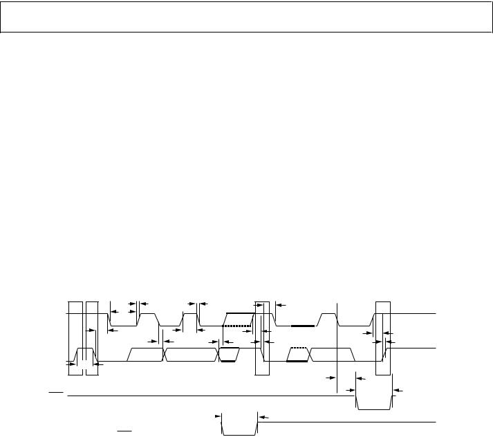
1 See Figure 3. High speed mode timing specification applies only to the AD5625RBRUZ-2/AD5625RBRUZ-2REEL7 and AD5665RBRUZ-2/AD5665RBRUZ-2REEL7. 2 CB refers to the capacitance on the bus line.
3The SDA and SCL timing is measured with the input filters enabled. Switching off the input filters improves the transfer rate but has a negative effect on the EMC behavior of the part.
4 Input filtering on the SCL and SDA inputs suppresses noise spikes that are less than 50 ns for fast mode or less than 10 ns for high speed mode.
|
t11 |
t12 |
|
t6 |
|
SCL |
t2 |
|
|
|
|
|
|
|
|
|
|
|
t6 |
t1 |
t5 |
|
t8 |
|
t4 |
t3 |
t10 |
|
t9 |
SDA |
|
|
|
|
|
|
t7 |
|
|
|
|
P |
S |
|
S |
t14 |
P |
LDAC* |
|
|
|
|
t13 |
|
|
|
|
|
|
|
|
|
|
t15 |
|
|
|
|
|
|
CLR |
|
|
|
||
|
|
|
|
||
*ASYNCHRONOUS LDAC UPDATE MODE.
Figure 3. 2-Wire Serial Interface Timing Diagram
06341-003
Rev. B | Page 9 of 36
AD5625R/AD5645R/AD5665R, AD5625/AD5665
ABSOLUTE MAXIMUM RATINGS
TA = 25°C, unless otherwise noted.
Table 6.
Parameter |
Rating |
|
|
VDD to GND |
−0.3 V to +7 V |
VOUT to GND |
−0.3 V to VDD + 0.3 V |
VREFIN/VREFOUT to GND |
−0.3 V to VDD + 0.3 V |
Digital Input Voltage to GND |
−0.3 V to VDD + 0.3 V |
Operating Temperature Range, Industrial |
−40°C to +105°C |
Storage Temperature Range |
−65°C to +150°C |
Junction Temperature (TJ maximum) |
150°C |
Power Dissipation |
(TJ max − TA)/θJA |
θJA Thermal Impedance |
|
LFCSP_WD (4-Layer Board) |
61°C/W |
TSSOP |
150.4°C/W |
Reflow Soldering Peak Temperature, |
260°C ± 5°C |
RoHS Compliant |
|
|
|
Stresses above those listed under Absolute Maximum Ratings may cause permanent damage to the device. This is a stress rating only; functional operation of the device at these or any other conditions above those indicated in the operational section of this specification is not implied. Exposure to absolute maximum rating conditions for extended periods may affect device reliability.
ESD CAUTION
Rev. B | Page 10 of 36
AD5625R/AD5645R/AD5665R, AD5625/AD5665
PIN CONFIGURATIONS AND FUNCTION DESCRIPTIONS
|
|
|
|
|
|
SCL |
||
|
LDAC |
|
1 |
|
14 |
|||
ADDR1 |
|
|
|
SDA |
||||
2 |
AD5625R/ |
13 |
||||||
|
VDD |
|
|
GND |
||||
|
3 |
12 |
||||||
|
|
|
|
AD5645R/ |
|
|
|
|
|
|
|
|
|
|
|
|
|
VOUTA |
4 |
AD5665R |
11 |
VOUTB |
||||
VOUTC |
|
TOP VIEW |
|
VOUTD |
||||
5 |
10 |
|||||||
|
|
|
|
(Not to Scale) |
|
|
|
|
|
POR |
6 |
9 |
CLR |
||||
|
|
|||||||
VREFIN/VREFOUT |
|
|
|
ADDR2 |
||||
7 |
|
8 |
||||||
|
|
|
|
|
|
|
|
|
06341-120
VOUTA |
|
|
|
VREFIN/VREFOUT |
|
1 |
AD5625R/ |
10 |
|||
VOUTB |
|
|
VDD |
||
2 |
AD5645R/ |
9 |
|||
GND |
|
|
SDA |
||
3 |
AD5665R |
8 |
|||
|
|
||||
VOUTC |
4 |
TOP VIEW |
7 |
SCL |
|
VOUTD |
|
(Not to Scale) |
|
ADDR |
|
5 |
6 |
||||
|
|||||
|
|
|
|
|
EXPOSED PAD TIED TO GND.
06341-122
Figure 4. Pin Configuration (14-Lead TSSOP), R Suffix Version
|
|
|
|
|
|
SCL |
|
||
|
LDAC |
|
1 |
|
14 |
|
|||
ADDR1 |
|
|
|
SDA |
|
||||
2 |
AD5625/ |
13 |
|
||||||
|
VDD |
|
|
GND |
|
||||
|
3 |
AD5665 |
12 |
|
|||||
VOUTA |
|
|
VOUTB |
|
|||||
4 |
TOP VIEW |
11 |
|
||||||
|
|
|
|||||||
VOUTC |
5 |
(Not to Scale) |
10 |
VOUTD |
|
||||
|
POR |
|
|
|
|
|
|
|
|
|
6 |
|
9 |
|
CLR |
|
-121 |
||
|
|
|
|
|
|
|
|
|
|
VREFIN |
|
|
|
ADDR2 |
06341 |
||||
7 |
|
8 |
|
||||||
|
|
|
|
|
|
|
|
|
|
Figure 5. Pin Configuration (14-Lead TSSOP)
Figure 6. Pin Configuration (10-Lead LFCSP), R Suffix Version
VOUTA |
|
|
|
VREFIN |
|
1 |
AD5625/ |
10 |
|
||
VOUTB |
|
|
VDD |
|
|
2 |
AD5665 |
9 |
|
||
GND |
|
|
SDA |
|
|
3 |
TOP VIEW |
8 |
|
||
|
|
|
|
|
|
VOUTC |
4 |
(Not to Scale) |
7 |
SCL |
|
VOUTD |
|
|
|
ADDR |
|
5 |
|
6 |
06341-123 |
||
|
|
|
|||
EXPOSED PAD TIED TO GND. |
|||||
Figure 7. Pin Configuration (10-Lead LFCSP)
Table 7. Pin Function Descriptions
Pin Number |
|
|
|
|
|
|
|
|
|
|
|
|
|
|
|
|
|
|
|
|
|
|
|
|
|
14-Lead |
10-Lead |
|
Mnemonic |
Description |
||||||||
|
|
|
|
|
|
|
|
|
|
|
|
|
1 |
N/A |
|
|
|
|
Pulsing this pin low allows any or all DAC registers to be updated if the input registers have new data. |
||||||
|
LDAC |
|
||||||||||
|
|
|
|
|
|
This allows simultaneous update of all DAC outputs. Alternatively, this pin can be tied permanently |
||||||
|
|
|
|
|
|
low. |
||||||
2 |
N/A |
|
ADDR1 |
Three-State Address Input. Sets the two least significant bits (Bit A1, Bit A0) of the 7-bit slave address |
||||||||
|
|
|
|
|
|
(see Table 9). |
||||||
3 |
9 |
|
VDD |
Power Supply Input. These parts can be operated from 2.7 V to 5.5 V, and the supply should be |
||||||||
|
|
|
|
|
|
decoupled with a 10 μF capacitor in parallel with a 0.1 μF capacitor to GND. |
||||||
4 |
1 |
|
VOUTA |
Analog Output Voltage from DAC A. The output amplifier has rail-to-rail operation. |
||||||||
5 |
4 |
|
VOUTC |
Analog Output Voltage from DAC C. The output amplifier has rail-to-rail operation. |
||||||||
6 |
N/A |
|
POR |
Power-On Reset Pin. Tying the POR pin to GND powers up the part to 0 V. Tying the POR pin to VDD |
||||||||
|
|
|
|
|
|
powers up the part to midscale. |
||||||
7 |
10 |
|
VREFIN/VREFOUT |
The AD56x5R have a common pin for reference input and reference output. When using the internal |
||||||||
|
|
|
|
|
|
reference, this is the reference output pin. When using an external reference, this is the reference |
||||||
|
|
|
|
|
|
input pin. The default for this pin is as a reference input. (The internal reference and reference output |
||||||
|
|
|
|
|
|
are only available on R suffix versions.) The AD56x5 has a reference input pin only. |
||||||
8 |
N/A |
ADDR2 |
Three-State Address Input. Sets Bit A3 and Bit A2 of the 7-bit slave address (see Table 9). |
|||||||||
9 |
N/A |
|
|
Asynchronous Clear Input. The |
|
input is falling-edge sensitive. While |
|
is low, all LDAC pulses |
||||
|
CLR |
|
CLR |
CLR |
||||||||
|
|
|
|
|
|
are ignored. When |
CLR |
is activated, zero scale is loaded to all input and DAC registers. This clears the |
||||
|
|
|
|
|
|
output to 0 V. The part exits clear code mode on the falling edge of the ninth clock pulse of the last |
||||||
|
|
|
|
|
|
byte of the valid write. If CLR is activated during a write sequence, the write is aborted. If CLR is |
||||||
|
|
|
|
|
|
activated during high speed mode, the part exits high speed mode. |
||||||
10 |
5 |
|
VOUTD |
Analog Output Voltage from DAC D. The output amplifier has rail-to-rail operation. |
||||||||
11 |
2 |
|
VOUTB |
Analog Output Voltage from DAC B. The output amplifier has rail-to-rail operation. |
||||||||
12 |
3 |
GND |
Ground Reference Point for All Circuitry on the Part. |
|||||||||
13 |
8 |
|
SDA |
Serial Data Line. This is used in conjunction with the SCL line to clock data into or out of the 16-bit |
||||||||
|
|
|
|
|
|
input register. It is a bidirectional, open-drain data line that should be pulled to the supply with an |
||||||
|
|
|
|
|
|
external pull-up resistor. |
||||||
14 |
7 |
|
SCL |
Serial Clock Line. This is used in conjunction with the SDA line to clock data into or out of the 16-bit |
||||||||
|
|
|
|
|
|
input register. |
||||||
N/A |
6 |
|
ADDR |
Three-State Address Input. Sets the two least significant bits (Bit A1, Bit A0) of the 7-bit slave address |
||||||||
|
|
|
|
|
|
(see Table 8). |
||||||
|
EPAD |
|
|
|
|
For the 10-lead LFCSP, the exposed pad must be tied to GND. |
||||||
|
|
|
|
|
|
|
|
|
|
|
|
|
Rev. B | Page 11 of 36
Loading...