


 Loading...
Analog Devices AD600JR-REEL, AD600JR, AD600JN, AD600AR-REEL7, AD600AR-REEL Datasheet
...a |
Dual, Low Noise, Wideband |
|
Variable Gain Amplifiers |
||
|
|
|
|
|
AD600/AD602* |
FEATURES
Two Channels with Independent Gain Control “Linear in dB” Gain Response
Two Gain Ranges: AD600: 0 dB to 40 dB
AD602: –10 dB to +30 dB Accurate Absolute Gain: 0.3 dB
Low Input Noise: 1.4 nV/√Hz
Low Distortion: –60 dBc THD at 1 V Output
High Bandwidth: DC to 35 MHz (–3 dB) Stable Group Delay: 2 ns
Low Power: 125 mW (Max) per Amplifier Signal Gating Function for Each Amplifier Drives High-Speed A/D Converters
MIL-STD-883-Compliant and DESC Versions Available
APPLICATIONS
Ultrasound and Sonar Time-Gain Control
High-Performance Audio and RF AGC Systems
Signal Measurement
PRODUCT DESCRIPTION
The AD600 and AD602 dual channel, low noise variable gain amplifiers are optimized for use in ultrasound imaging systems, but are applicable to any application requiring very precise gain, low noise and distortion, and wide bandwidth. Each independent channel provides a gain of 0 dB to +40 dB in the AD600 and –10 dB to +30 dB in the AD602. The lower gain of the AD602 results in an improved signal-to-noise ratio at the output. However, both products have the same 1.4 nV/√Hz input noise spectral density. The decibel gain is directly proportional to the control voltage, is accurately calibrated, and is supplyand temperature-stable.
To achieve the difficult performance objectives, a proprietary circuit form—the X-AMP®—has been developed. Each channel of the X-AMP comprises a variable attenuator of 0 dB to –42.14 dB followed by a high speed fixed gain amplifier. In this way, the amplifier never has to cope with large inputs, and can benefit from the use of negative feedback to precisely define the gain and dynamics. The attenuator is realized as a seven-stage R-2R ladder network having an input resistance of 100 Ω, lasertrimmed to ±2%. The attenuation between tap points is 6.02 dB; the gain-control circuit provides continuous interpolation between these taps. The resulting control function is linear in dB.
X-AMP is a registered trademark of Analog Devices, Inc. *Patented.
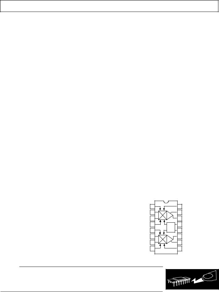
FUNCTIONAL BLOCK DIAGRAM
|
|
|
|
|
|
GAT1 |
|
SCALING |
|
PRECISION PASSIVE |
GATING |
||||
|
INPUT ATTENUATOR |
||||||
REFERENCE |
INTERFACE |
||||||
|
|
|
|||||
C1HI |
|
|
|
|
|
|
|
VG |
|
|
|
|
|
A1OP |
|
C1LO |
|
|
|
|
|
|
|
GAIN CONTROL |
|
|
|
A1CM |
|||
|
|
|
|
||||
INTERFACE |
|
|
|
|
RF2 |
||
|
|
|
|
|
|
||
|
|
|
|
|
|
2.24k (AD600) |
|
0dB |
–12.04dB |
–22.08dB |
–36.12dB |
694 (AD602) |
|||
–6.02dB |
–18.06dB |
–30.1dB |
–42.14dB |
RF1 |
|||
A1HI |
|
|
|
|
|
20 |
|
|
|
|
|
|
|
FIXED-GAIN |
|
A1LO |
|
|
|
|
|
AMPLIFIER |
|
500 |
R – 2R LADDER NETWORK |
62.5 |
41.07dB(AD600) |
||||
|
|
|
|
|
|
31.07(AD602) |
|
The gain-control interfaces are fully differential, providing an input resistance of ~15 MΩ and a scale factor of 32 dB/V (that is, 31.25 mV/dB) defined by an internal voltage reference. The response time of this interface is less than 1 µs. Each channel also has an independent gating facility that optionally blocks signal transmission and sets the dc output level to within a few millivolts of the output ground. The gating control input is TTL and CMOS compatible.
The maximum gain of the AD600 is 41.07 dB, and that of the AD602 is 31.07 dB; the –3 dB bandwidth of both models is nominally 35 MHz, essentially independent of the gain. The signal-to-noise ratio (SNR) for a 1 V rms output and a 1 MHz noise bandwidth is typically 76 dB for the AD600 and 86 dB for the AD602. The amplitude response is flat within ±0.5 dB from 100 kHz to 10 MHz; over this frequency range the group delay varies by less than ±2 ns at all gain settings.
Each amplifier channel can drive 100 Ω load impedances with low distortion. For example, the peak specified output is ±2.5 V minimum into a 500 Ω load, or ± 1 V into a 100 Ω load. For a 200 Ω load in shunt with 5 pF, the total harmonic distortion for a ±1 V sinusoidal output at 10 MHz is typically –60 dBc.
The AD600J and AD602J are specified for operation from 0°C to 70°C, and are available in both 16-lead plastic DIP (N) and 16-lead SOIC (R). The AD600A and AD602A are specified for operation from –40°C to +85°C and are available in both 16-lead cerdip (Q) and 16-lead SOIC (R).
The AD600S and AD602S are specified for operation from –55°C to +125°C and are available in a 16-lead cerdip (Q) package and are MIL-STD-883 compliant. The AD600S and AD602S are also available under DESC SMD 5962-94572.
REV. B
Information furnished by Analog Devices is believed to be accurate and reliable. However, no responsibility is assumed by Analog Devices for its use, nor for any infringements of patents or other rights of third parties which may result from its use. No license is granted by implication or otherwise under any patent or patent rights of Analog Devices.
One Technology Way, P.O. Box 9106, Norwood, MA 02062-9106, U.S.A.
Tel: 781/329-4700 |
World Wide Web Site: http://www.analog.com |
Fax: 781/326-8703 |
© Analog Devices, Inc., 2001 |
AD600/AD602–SPECIFICATIONS (Each amplifier section, at TA = 25 C, VS = 5 V, –625 mV ≤ VG ≤ +625 mV, RL = 500 , and CL = 5 pF, unless otherwise noted. Specifications for AD600 and AD602 are identical unless otherwise noted.)
|
|
AD600J/AD602J |
AD600A/AD602A |
|
||||
Parameter |
Conditions |
Min |
Typ |
Max |
Min |
Typ |
Max |
Unit |
|
|
|
|
|
|
|
|
|
INPUT CHARACTERISTICS |
|
|
|
|
|
|
|
Ω |
Input Resistance |
Pins 2 to 3; Pins 6 to 7 |
98 |
100 |
102 |
95 |
100 |
105 |
|
Input Capacitance |
|
|
2 |
|
|
2 |
|
pF |
Input Noise Spectral Density1 |
RS = 50 Ω, Maximum Gain |
|
1.4 |
|
|
1.4 |
|
nV/√Hz |
Noise Figure |
|
5.3 |
|
|
5.3 |
|
dB |
|
|
RS = 200 Ω, Maximum Gain |
|
2 |
|
|
2 |
|
dB |
Common-Mode Rejection Ratio |
f = 100 kHz |
|
30 |
|
|
30 |
|
dB |
|
|
|
|
|
|
|
|
|
OUTPUT CHARACTERISTICS |
|
|
|
|
|
|
|
|
–3 dB Bandwidth |
VOUT = 100 mV rms |
|
35 |
|
|
35 |
|
MHz |
Slew Rate |
|
|
275 |
|
|
275 |
|
V/µs |
Peak Output2 |
RL ≥ 500 Ω |
±2.5 |
±3 |
|
±2.5 |
±3 |
|
V |
Output Impedance |
f ≤ 10 MHz |
|
2 |
|
|
2 |
|
Ω |
Output Short-Circuit Current |
|
|
50 |
|
|
50 |
|
mA |
Group Delay Change vs. Gain |
f = 3 MHz; Full Gain Range |
|
±2 |
|
|
±2 |
|
ns |
Group Delay Change vs. Frequency |
VG = 0 V, f = 1 MHz to 10 MHz |
|
±2 |
|
|
±2 |
|
ns |
Total Harmonic Distortion |
RL= 200 Ω, VOUT = ±1 V Peak, Rpd = 1 kΩ |
|
–60 |
|
|
–60 |
|
dBc |
ACCURACY |
|
|
|
|
|
|
|
|
AD600 |
|
|
|
|
|
|
|
|
Gain Error |
0 dB to 3 dB Gain |
0 |
+0.5 |
+1 |
–0.5 |
+0.5 |
+1.5 |
dB |
|
3 dB to 37 dB Gain |
–0.5 |
±0.2 |
+0.5 |
–1.0 |
±0.2 |
+1.0 |
dB |
Maximum Output Offset Voltage3 |
37 dB to 40 dB Gain |
–1 |
–0.5 |
0 |
–1.5 |
–0.5 |
+0.5 |
dB |
VG = –625 mV to +625 mV |
|
10 |
50 |
|
10 |
65 |
mV |
|
Output Offset Variation |
VG = –625 mV to +625 mV |
|
10 |
50 |
|
10 |
65 |
mV |
AD602 |
|
|
|
|
|
|
|
|
Gain Error |
–10 dB to –7 dB Gain |
0 |
+0.5 |
+1 |
–0.5 |
+0.5 |
+1.5 |
dB |
|
–7 dB to +27 dB Gain |
–0.5 |
±0.2 |
+0.5 |
–1.0 |
±0.2 |
+1.0 |
dB |
Maximum Output Offset Voltage3 |
27 dB to 30 dB Gain |
–1 |
–0.5 |
0 |
–1.5 |
–0.5 |
+0.5 |
dB |
VG = –625 mV to +625 mV |
|
5 |
30 |
|
10 |
45 |
mV |
|
Output Offset Variation |
VG = –625 mV to +625 mV |
|
5 |
30 |
|
10 |
45 |
mV |
GAIN CONTROL INTERFACE |
|
|
|
|
|
|
|
|
Gain Scaling Factor |
3 dB to 37 dB (AD600); –7 dB to +27 dB (AD602) |
31.7 |
32 |
32.3 |
30.5 |
32 |
33.5 |
dB/V |
Common-Mode Range |
|
–0.75 |
|
+2.5 |
–0.75 |
|
+2.5 |
V |
Input Bias Current |
|
|
0.35 |
1 |
|
0.35 |
1 |
µA |
Input Offset Current |
|
|
10 |
50 |
|
10 |
50 |
nA |
Differential Input Resistance |
Pins 1 to 16; Pins 8 to 9 |
|
15 |
|
|
15 |
|
MΩ |
Response Rate |
Full 40 dB Gain Change |
|
40 |
|
|
40 |
|
dB/µs |
|
|
|
|
|
|
|
|
|
SIGNAL GATING INTERFACE |
|
|
|
|
|
|
|
|
Logic Input “LO” (Output ON) |
|
|
|
0.8 |
|
|
0.8 |
V |
Logic Input “HI” (Output OFF) |
|
2.4 |
|
|
2.4 |
|
|
V |
Response Time |
ON to OFF, OFF to ON |
|
0.3 |
|
|
0.3 |
|
µs |
Input Resistance |
Pins 4 to 3; Pins 5 to 6 |
|
30 |
|
|
30 |
|
kΩ |
Output Gated OFF |
|
|
±10 |
|
|
±10 |
|
|
Output Offset Voltage |
|
|
100 |
|
400 |
mV |
||
Output Noise Spectral Density |
|
|
65 |
|
|
65 |
|
nV/√Hz |
Signal Feedthrough @ 1 MHz |
|
|
|
|
|
|
|
|
AD600 |
|
|
–80 |
|
|
–80 |
|
dB |
AD602 |
|
|
–70 |
|
|
–70 |
|
dB |
|
|
|
|
|
|
|
|
|
POWER SUPPLY |
|
±4.75 |
|
±5.25 |
±4.75 |
|
±5.25 |
|
Specified Operating Range |
|
|
|
V |
||||
Quiescent Current |
|
|
11 |
12.5 |
|
22 |
28 |
mA |
|
|
|
|
|
|
|
|
|
NOTES
1Typical open or short-circuited input; noise is lower when system is set to maximum gain and input is short-circuited. This figure includes the effects of both voltage and current noise sources.
2Using resistive loads of 500 Ω or greater, or with the addition of a 1 kΩ pull-down resistor when driving lower loads.
3The dc gain of the main amplifier in the AD600 is X113; thus an input offset of only 100 µV becomes an 11.3 mV output offset. In the AD602, the amplifier’s gain is X35.7; thus, an input offset of 100 µV becomes a 3.57 mV output offset.
Specifications shown in boldface are tested on all production units at final electrical test. Results from those tests are used to calculate outgoing quality levels. All min and max specifications guaranteed, although only those shown in boldface are tested on all production units.
Specifications subject to change without notice.
–2– |
REV. B |
AD600/AD602
ABSOLUTE MAXIMUM RATINGS1 |
|
Supply Voltage ±VS . . . . . . . . . . . . . . . . . . . . |
. . . . . . . ±7.5 V |
Input Voltages |
±VS |
Pins 1, 8, 9, 16 . . . . . . . . . . . . . . . . . . . . . . |
|
Pins 2, 3, 6, 7 . . . . . . . . . . . . . . . . . . . . . . |
±2 V Continuous |
. . . . . . . . . . . . . . . . . . . . . . . |
. . ±VS for 10 ms |
Pins 4, 5 . . . . . . . . . . . . . . . . . . . . . . . . . . . |
. . . . . . . . . . ±VS |
Internal Power Dissipation2 . . . . . . . . . . . . . . |
. . . . . . 600 mW |
Operating Temperature Range (J) . . . . . . . . . |
. . . 0°C to 70°C |
Operating Temperature Range (A) . . . . . . . . |
–40°C to +85°C |
Operating Temperature Range (S) . . . . . . . |
–55°C to +125°C |
Storage Temperature Range . . . . . . . . . . . . |
–65°C to +150°C |
Lead Temperature Range (Soldering 60 sec) . |
. . . . . . . . 300°C |
NOTES
1Stresses above those listed under Absolute Maximum Ratings may cause permanent damage to the device. This is a stress rating only; functional operation of the device at these or any other conditions above those indicated in the operational section of this specification is not implied. Exposure to absolute maximum rating conditions for extended periods may affect device reliability.
2Thermal Characteristics:
16-Lead Plastic Package: θJA = 85°C/W
16-Lead SOIC Package: θJA = 100°C/W
16-Lead Cerdip Package: θJA = 120°C/W
ORDERING GUIDE
|
Gain |
Temperature |
Package |
Model |
Range |
Range |
Option1 |
AD600AQ |
0 dB to 40 dB |
–40°C to +85°C |
Q-16 |
AD600AR |
0 dB to 40 dB |
–40°C to +85°C |
R-16 |
AD600AR-REEL |
0 dB to 40 dB |
–40°C to +85°C |
13" Reel |
AD600AR-REEL7 |
0 dB to 40 dB |
–40°C to +85°C |
7" Reel |
AD600JN |
0 dB to 40 dB |
0°C to 70°C |
N-16 |
AD600JR |
0 dB to 40 dB |
0°C to 70°C |
R-16 |
AD600JR-REEL |
0 dB to 40 dB |
0°C to 70°C |
13" Reel |
AD600JR-REEL7 |
0 dB to 40 dB |
0°C to 70°C |
7" Reel |
AD600SQ/883B2 |
0 dB to 40 dB |
–55°C to +125°C |
Q-16 |
AD602AQ |
–10 dB to +30 dB |
–40°C to +85°C |
Q-16 |
AD602AR |
–10 dB to +30 dB |
–40°C to +85°C |
R-16 |
AD602AR-REEL |
–10 dB to +30 dB |
–40°C to +85°C |
13" Reel |
AD602AR-REEL7 |
–10 dB to +30 dB |
–40°C to +85°C |
7" Reel |
AD602JN |
–10 dB to +30 dB |
0°C to 70°C |
N-16 |
AD602JR |
–10 dB to +30 dB |
0°C to 70°C |
R-16 |
AD602JR-REEL |
–10 dB to +30 dB |
0°C to 70°C |
13" Reel |
AD602JR-REEL7 |
–10 dB to +30 dB |
0°C to 70°C |
7" Reel |
AD602SQ/883B3 |
–10 dB to +30 dB |
–55°C to +150°C |
Q-16 |
NOTES
1N = Plastic DIP; Q = Cerdip; R = Small Outline IC (SOIC).
2Refer to AD600/AD602 Military data sheet. Also available as 5962-9457201MEA. 3Refer to AD600/AD602 Military data sheet. Also available as 5962-9457202MEA.
PIN FUNCTION DESCRIPTIONS
Pin |
Mnemonic |
|
Description |
|
|
|
|
1 |
C1LO |
|
CH1 Gain-Control Input “LO” (Positive |
|
|
|
Voltage Reduces CH1 Gain). |
2 |
A1HI |
|
CH1 Signal Input “HI” (Positive Voltage |
|
|
|
Increases CH1 Output). |
3 |
A1LO |
|
CH1 Signal Input “LO” (Usually Taken to |
|
|
|
CH1 Input Ground) |
4 |
GAT1 |
|
CH1 Gating Input (A Logic “HI” Shuts Off |
|
|
|
CH1 Signal Path). |
5 |
GAT2 |
|
CH2 Gating Input (A Logic “HI” Shuts Off |
|
|
|
CH2 Signal Path). |
6 |
A2LO |
|
CH2 Signal Input “LO” (Usually Taken to |
|
|
|
CH2 Input Ground). |
7 |
A2HI |
|
CH2 Signal Input “HI” (Positive Voltage |
|
|
|
Increases CH2 Output). |
8 |
C2LO |
|
CH2 Gain-Control Input “LO” (Positive |
|
|
|
Voltage Reduces CH2 Gain). |
9 |
C2HI |
|
CH2 Gain-Control Input “HI” (Positive |
|
|
|
Voltage Increases CH2 Gain). |
10 |
A2CM |
|
CH2 Common (Usually Taken to CH2 |
|
|
|
Output Ground). |
11 |
A2OP |
|
CH2 Output. |
12 |
VNEG |
|
Negative Supply for Both Amplifiers. |
13 |
VPOS |
|
Positive Supply for Both Amplifiers. |
14 |
A1OP |
|
CH1 Output. |
15 |
A1CM |
|
CH1 Common (Usually Taken to CH1 |
|
|
|
Output Ground). |
16 |
C1HI |
|
CH1 Gain-Control Input “HI” (Positive |
|
|
|
Voltage Increases CH1 Gain). |
|
|
|
|
|
|
CONNECTION DIAGRAM |
|
|
16-Lead Plastic DIP (N) Package |
||
|
16-Lead Plastic SOIC (R) Package |
||
|
|
16-Lead Cerdip (Q) Package |
|
C1LO |
1 |
|
|
16 |
C1HI |
A1HI |
2 |
+ |
A1 |
15 |
A1CM |
|
|
|
|
||
|
|
|
|
|
|
A1LO |
3 |
– |
|
14 |
A1OP |
|
|
|
|
|
|
GAT1 |
4 |
|
REF |
13 |
VPOS |
|
|
|
|
|
|
GAT2 |
5 |
|
|
12 |
VNEG |
A2LO |
6 |
– |
A2 |
11 |
A2OP |
|
|
|
|
|
|
A2HI |
7 |
+ |
|
10 |
A2CM |
|
|
|
|
|
|
C2LO |
8 |
AD600 / AD602 |
9 |
C2HI |
|
|
|
|
|
||
CAUTION
ESD (electrostatic discharge) sensitive device. Electrostatic charges as high as 4000 V readily accumulate on the human body and test equipment and can discharge without detection. Although the AD600/AD602 features proprietary ESD protection circuitry, permanent damage may occur on devices subjected to high-energy electrostatic discharges. Therefore, proper ESD precautions are recommended to avoid performance degradation or loss of functionality.
WARNING!
ESD SENSITIVE DEVICE
REV. B |
–3– |

AD600/AD602–Typical Performance Characteristics
|
0.45 |
|
|
|
|
|
|
|
|
|
|
|
|
|
|
|
|
|
|
|
0.35 |
|
|
|
|
|
|
|
|
|
|
|
|
|
|
|
|
|
|
dB |
0.25 |
|
|
|
|
|
|
|
|
|
|
|
|
|
|
|
|
||
0.15 |
|
|
|
|
|
|
|
|
|
|
|
|
|
|
|
|
|
||
– |
–0.05 |
|
|
|
|
|
|
|
|
ERROR |
|
|
|
|
|
|
|
|
|
GAIN |
0.05 |
|
|
|
|
|
|
|
|
–0.15 |
|
|
|
|
|
|
|
|
|
|
|
|
|
|
|
|
|
|
|
|
–0.25 |
|
|
|
|
|
|
|
|
|
|
|
|
|
|
|
|
|
|
|
–0.35 |
|
|
|
|
|
|
|
|
|
|
|
|
|
|
|
|
|
|
|
–0.45 |
|
|
|
|
|
|
|
|
|
|
|
|
|
|
|
|
|
|
|
–0.7 –0.5 –0.3 –0.1 0.1 0.3 0.5 0.7 |
||||||||
|
|
GAIN CONTROL VOLTAGE – Volts |
|||||||
TPC 1. Gain Error vs. Gain Control
Voltage |
|
|
|
|
|
|
||
|
10.0 |
|
|
|
|
|
|
|
|
9.8 |
|
|
|
|
|
|
|
|
9.6 |
|
|
|
|
|
|
|
ns |
9.4 |
|
|
|
|
|
|
|
– |
9.2 |
|
|
|
|
|
|
|
DELAY |
|
|
|
|
|
|
|
|
9.0 |
|
|
|
|
|
|
|
|
|
|
|
|
|
|
|
|
|
GROUP |
8.8 |
|
|
|
|
|
|
|
8.6 |
|
|
|
|
|
|
|
|
|
8.4 |
|
|
|
|
|
|
|
|
8.2 |
|
|
|
|
|
|
|
|
8.0 |
|
|
|
|
|
|
|
|
–0.7 |
–0.5 |
–0.3 |
–0.1 |
0.1 |
0.3 |
0.5 |
0.7 |
GAIN CONTROL VOLTAGE – Volts
TPC 4. AD600 and AD602 Typical Group Delay vs. VC
|
102 |
|
|
|
|
101 |
GAIN = 40dB |
|
|
|
|
|
|
|
– |
100 |
|
|
|
99 |
|
|
|
|
IMPEDANCE |
|
|
|
|
98 |
|
GAIN = 20dB |
|
|
|
|
|
||
97 |
|
GAIN = 0dB |
|
|
96 |
|
|
|
|
INPUT |
|
|
|
|
95 |
|
|
|
|
|
|
|
|
|
|
94 |
|
|
|
|
93 |
|
|
|
|
92 |
|
|
|
|
100k |
1M |
10M |
100M |
|
|
FREQUENCY – Hz |
|
|
TPC 7. Input Impedance vs. Frequency
20dB |
|
|
|
17dB |
|
|
|
0 |
|
|
|
–45 |
|
|
|
–90 |
|
|
|
100k |
1M |
10M |
100M |
FREQUENCY – Hz
TPC 2. AD600 Frequency and Phase Response vs. Gain
VG = 0V 10dB/DIV CENTER FREQ 1MHz 10kHz/DIV
TPC 5. Third Order Intermodula-
tion Distortion, VOUT = 2 V p-p, |
|
|||||||
RL = 500 Ω |
|
|
|
|
|
|
||
|
6 |
|
|
|
|
|
|
|
– mV |
5 |
|
|
|
|
|
|
|
4 |
|
|
|
AD600 |
|
|
|
|
VOLTAGE |
3 |
|
|
|
|
|
|
|
2 |
|
|
AD602 |
|
|
|
||
|
|
|
|
|
|
|||
OFFSET |
1 |
|
|
|
|
|
|
|
0 |
|
|
|
|
|
|
|
|
|
|
|
|
|
|
|
|
|
OUTPUT |
–1 |
|
|
|
|
|
|
|
–2 |
|
|
|
|
|
|
|
|
–3 |
|
|
|
|
|
|
|
|
|
|
|
|
|
|
|
|
|
|
–4 |
|
|
|
|
|
|
|
|
–0.7 |
–0.5 |
–0.3 |
–0.1 |
0.1 |
0.3 |
0.5 |
0.7 |
GAIN CONTROL VOLTAGE – Volts
TPC 8. Output Offset vs. Gain Control Voltage (Control Channel Feedthrough)
10dB |
|
|
|
7dB |
|
|
|
0 |
|
|
|
–45 |
|
|
|
–90 |
|
|
|
100k |
1M |
10M |
100M |
FREQUENCY – Hz
TPC 3. AD602 Frequency and Phase Response vs. Gain
Volts |
–1.0 |
|
|
|
|
|
|
–1.2 |
|
|
|
|
|
|
|
– |
–1.4 |
|
|
|
|
|
|
LIMIT |
|
|
|
|
|
|
|
–1.6 |
|
|
|
|
|
|
|
|
|
|
|
|
|
|
|
VOLTAGE |
–1.8 |
|
|
|
|
|
|
–2.0 |
|
|
|
|
|
|
|
–2.2 |
|
|
|
|
|
|
|
OUTPUT |
–2.4 |
|
|
|
|
|
|
–2.6 |
|
|
|
|
|
|
|
–2.8 |
|
|
|
|
|
|
|
NEGATIVE |
|
|
|
|
|
|
|
–3.0 |
|
|
|
|
|
|
|
–3.2 |
|
|
|
|
|
|
|
–3.4 |
|
|
|
|
|
|
|
|
50 |
100 |
200 |
500 |
1000 |
2000 |
|
|
0 |
LOAD RESISTANCE –
TPC 6. Typical Output Voltage vs. Load Resistance (Negative Output Swing Limits First)
|
1V VOUT |
1µs |
|
100 |
|
OUTPUT |
90 |
|
|
|
|
INPUT |
10 |
|
0% |
|
1V VC
TPC 9. Gain Control Channel Response Time. Top: Output Voltage, 2 V max, Bottom: Gain Control Voltage VC = ±625 mV
–4– |
REV. B |
AD600/AD602
|
|
50mV |
OUTPUT |
100 |
|
90 |
|
|
INPUT |
10 |
|
|
0% |
|
|
5V |
100ns |
|
|
|
TPC 10. Gating Feedthrough to Output, Gating Off to On
50mV
OUTPUT |
100 |
90 |
|
INPUT |
10 |
|
0% |
5V |
100ns |
TPC 11. Gating Feedthrough to Output, Gating On to Off
|
1V |
|
|
100 |
|
OUTPUT |
90 |
|
|
|
|
INPUT |
10 |
|
0% |
|
|
|
100mV |
500ns |
|
|
|
TPC 12. Transient Response,
Medium and High Gain
OUTPUT |
|
500mV |
OUTPUT |
|
1V |
100 |
|
100 |
|
||
|
90 |
|
|
90 |
|
INPUT |
10 |
|
INPUT |
10 |
|
|
0% |
|
|
0% |
|
|
1V |
200ns |
|
200mV |
500ns |
TPC 13. Input Stage Overload |
TPC 14. Output Stage Overload |
Recovery Time |
Recovery Time |
|
|
500mV |
|
|
100 |
|
|
OUTPUT |
90 |
|
|
|
|
||
INPUT |
10 |
|
|
0% |
|
||
1V |
500ns |
||
|
TPC 15. Transient Response
Minimum Gain
|
10 |
|
|
|
|
|
|
5 |
AD600: G = 20dB |
|
|
|
|
|
AD602: G = 10dB |
|
|
|
||
|
|
|
|
|
||
|
0 |
BOTH: VCM = 100mV RMS |
|
|
||
|
|
VS = |
5V |
|
|
|
|
–5 |
RL = 500 |
|
|
|
|
dB |
–10 |
TA = 25 C |
|
|
|
|
– |
–15 |
|
|
|
|
|
CMRR |
|
|
|
|
|
|
–20 |
|
AD600 |
|
|
|
|
|
|
|
|
|
|
|
|
–25 |
|
|
|
|
|
|
–30 |
|
|
AD602 |
|
|
|
–35 |
|
|
|
||
|
|
|
|
|
|
|
|
–40 |
|
|
|
|
|
|
1k |
10k |
100k |
1M |
10M |
100M |
|
|
FREQUENCY – Hz |
|
|
||
TPC 16. CMRR vs. Frequency
|
20 |
|
|
|
|
10 |
|
|
|
|
0 |
|
|
|
|
–10 |
AD600 |
|
|
|
|
|
|
|
– dB |
–20 |
|
|
|
–30 |
|
|
|
|
PSRR |
|
AD602 |
|
|
–40 |
|
|
||
|
|
|
||
|
–50 |
|
AD600: G = 40dB |
|
|
|
AD602: G = 30dB |
|
|
|
|
|
|
|
|
–60 |
|
BOTH: RL = 500 |
|
|
–70 |
|
VIN = 0V |
|
|
|
RS = 50 |
|
|
|
|
|
|
|
|
–80 |
|
|
|
|
100k |
1M |
10M |
100M |
|
|
FREQUENCY – Hz |
|
|
TPC 17. PSRR vs. Frequency
|
10 |
|
|
|
|
|
0 |
AD600: CH1 G = 40dB, VIN = 0 |
|
||
|
|
CH2 G = 20dB, VIN = 100mV |
|||
|
–10 |
AD602: CH1 G = 30dB, VIN = 0 |
|
||
|
|
|
CH2 G = 0dB, VIN = 316mV |
||
– dB |
–20 |
BOTH: VOUT = 1V RMS1, RS = 50 , |
|||
|
|
RL = 500 |
CH1 V |
} |
|
–30 |
CROSSTALK = 20log { CH2 VOUTIN |
||||
CROSSTALK |
–40 |
|
|
|
|
–50 |
|
|
AD600 |
|
|
|
|
|
|
||
–60 |
|
|
|
|
|
|
|
|
|
|
|
|
–70 |
|
|
AD602 |
|
|
|
|
|
||
|
–80 |
|
|
|
|
|
–90 |
|
|
|
|
|
100k |
1M |
10M |
100M |
|
|
|
|
FREQUENCY – Hz |
|
|
TPC 18. Crosstalk Between A1 and A2 vs. Frequency
REV. B |
–5– |
AD600/AD602
THEORY OF OPERATION
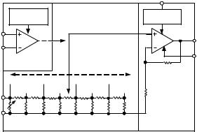
The AD600 and AD602 have the same general design and features. They comprise two fixed gain amplifiers, each preceded by a voltage-controlled attenuator of 0 dB to 42.14 dB with independent control interfaces, each having a scaling factor of 32 dB per volt. The gain of each amplifier in the AD600 is laser trimmed to 41.07 dB (X113), thus providing a control range of –1.07 dB to 41.07 dB (0 dB to 40 dB with overlap), while the AD602 amplifiers have a gain of 31.07 dB (X35.8) and provide an overall gain of –11.07 dB to 31.07 dB (–10 dB to 30 dB with overlap).
The advantage of this topology is that the amplifier can use negative feedback to increase the accuracy of its gain; also, since the amplifier never has to handle large signals at its input, the distortion can be very low. A further feature of this approach is that the small-signal gain and phase response, and thus the pulse response, are essentially independent of gain.
The following discussion describes the AD600. Figure 1 is a simplified schematic of one channel. The input attenuator is a seven-section R-2R ladder network, using untrimmed resistors of nominally R = 62.5 Ω, which results in a characteristic resistance of 125 Ω ± 20%. A shunt resistor is included at the input and laser trimmed to establish a more exact input resistance of 100 Ω ± 2%, which ensures accurate operation (gain and HP corner frequency) when used in conjunction with external resistors or capacitors.
|
|
|
|
|
|
GAT1 |
|
SCALING |
|
PRECISION PASSIVE |
GATING |
||||
|
INPUT ATTENUATOR |
||||||
REFERENCE |
INTERFACE |
||||||
|
|
|
|||||
C1HI |
|
|
|
|
|
|
|
VG |
|
|
|
|
|
A1OP |
|
C1LO |
|
|
|
|
|
|
|
GAIN CONTROL |
|
|
|
A1CM |
|||
|
|
|
|
||||
INTERFACE |
|
|
|
|
RF2 |
||
|
|
|
|
|
|
||
|
|
|
|
|
|
2.24k (AD600) |
|
0dB |
–12.04dB |
–22.08dB |
–36.12dB |
694 (AD602) |
|||
–6.02dB |
–18.06dB |
–30.1dB |
–42.14dB |
RF1 |
|||
A1HI |
|
|
|
|
|
20 |
|
|
|
|
|
|
|
FIXED-GAIN |
|
A1LO |
|
|
|
|
|
AMPLIFIER |
|
500 |
R – 2R LADDER NETWORK |
62.5 |
41.07dB(AD600) |
||||
|
|
|
|
|
|
31.07(AD602) |
|
Figure 1. Simplified Block Diagram of Single Channel of the AD600 and AD602
The nominal maximum signal at input A1HI is 1 V rms (±1.4 V peak) when using the recommended ± 5 V supplies, although operation to ±2 V peak is permissible with some increase in HF distortion and feedthrough. Each attenuator is provided with a separate signal “LO” connection, for use in rejecting commonmode, the voltage between input and output grounds. Circuitry is included to provide rejection of up to ±100 mV.
The signal applied at the input of the ladder network is attenuated by 6.02 dB by each section; thus, the attenuation to each of the taps is progressively 0, 6.02, 12.04, 18.06, 24.08, 30.1, 36.12 and 42.14 dB. A unique circuit technique is employed to interpolate between these tap points, indicated by the “slider” in Figure 1, providing continuous attenuation from 0 dB to 42.14 dB.
It will help, in understanding the AD600, to think in terms of a mechanical means for moving this slider from left to right; in fact, it is voltage controlled. The details of the control interface are discussed later. Note that the gain is at all times exactly determined, and a linear decibel relationship is automatically guaranteed between the gain and the control parameter which determines the position of the slider. In practice, the gain deviates from the ideal law, by about ±0.2 dB peak (see, for example, Figure 6).
Note that the signal inputs are not fully differential: A1LO and A1CM (for CH1) and A2LO and A2CM (for CH2) provide separate access to the input and output grounds. This recognizes the practical fact that even when using a ground plane, small differences will arise in the voltages at these nodes. It is important that A1LO and A2LO be connected directly to the input ground(s); significant impedance in these connections will reduce the gain accuracy. A1CM and A2CM should be connected to the load ground(s).
Noise Performance
An important reason for using this approach is the superior noise performance that can be achieved. The nominal resistance seen at the inner tap points of the attenuator is 41.7 Ω (one third
of 125 Ω), which exhibits a Johnson noise spectral density (NSD) of 0.84 nV/√Hz (that is, √4kTR) at 27°C, which is a large fraction
of the total input noise. The first stage of the amplifier contributes a further 1.12 nV/√Hz, for a total input noise of 1.4 nV/√Hz.
The noise at the 0 dB tap depends on whether the input is short-circuited or open-circuited: when shorted, the minimum NSD of 1.12 nV/√Hz is achieved; when open, the resistance of 100 Ω at the first tap generates 1.29 nV/√Hz, so the noise increases to a total of 1.71 nV/√Hz. (This last calculation would be important if the AD600 were preceded, for example, by a 900 Ω resistor to allow operation from inputs up to ±10 V rms. However, in most cases the low impedance of the source will limit the maximum noise resistance.)
It will be apparent from the foregoing that it is essential to use a low resistance in the design of the ladder network to achieve low noise. In some applications this may be inconvenient, requiring the use of an external buffer or preamplifier. However, very few amplifiers combine the needed low noise with low distortion at maximum input levels, and the power consumption needed to achieve this performance is fundamentally required to be quite high (due to the need to maintain very low resistance values while also coping with large inputs). On the other hand, there is little value in providing a buffer with high input impedance, since the usual reason for this—the minimization of loading of a high resistance source—is not compatible with low noise.
Apart from the small variations just discussed, the signal-to- noise (S/N) ratio at the output is essentially independent of the attenuator setting, since the maximum undistorted output is 1 V rms and the NSD at the output of the AD600 is fixed at 113 times 1.4 nV/√Hz, or 158 nV/√Hz. Thus, in a 1 MHz bandwidth, the output S/N ratio would be 76 dB. The input NSD of the AD600 and AD602 are the same, but because of the 10 dB lower gain in the AD602’s fixed amplifier, its output S/N ratio is 10 dB better, or 86 dB in a 1 MHz bandwidth.
–6– |
REV. B |
Loading...